692 Brazilian Journal of Physics, vol. 34, no. 2B, June, 2004
Some Key Issues on the Optimization of Multiple Quantum
Well Structures for Amplitude Modulation
C.V-B. Tribuzy, M. P. Pires, B. Yavich
∗, and P. L. Souza
Laborat´orio de Semicondutores, Centro de Estudos em Telecomunicac¸ ˜oes, Pontif´ıcia Universidade Cat´olica do Rio de Janeiro, Rua Marquˆes de S˜ao Vicente 225, Rio de Janeiro, 22453-900, Brasil
Received on 31 March, 2003
Main parameters of InGaAs/InAlAs multiple quantum well amplitude modulators, such as contrast ratio, inser-tion loss and chirp parameter, were calculated in order to find a quantum well structure which optimizes them. The parameters were estimated from the theoretical absorption curves, which were calculated for different val-ues of applied reverse bias and were compared with experimental data. A study of the device parameters as a function of the Ga content and operation voltage was performed. The study showed that optimum values for the modulator parameters cannot be obtained simultaneously. The influence of the residual doping level and the applied pre-bias are emphasized.
1
Introduction
Much attention has been driven to the InGaAs/InAlAs mul-tiple quantum well (MQW) system due to its suitable prop-erties for the development of amplitude modulators to be used in telecommunication [1-4]. This system can produce structures that operate at 1.55µm and it can be grown on InP substrates for optoelectronic integration. Another character-istic is the lower valence band offset compared to that of the InGaAs/InP system, which is desirable to avoid satura-tion effects due to a long hole escape time from the quantum wells (QWs). Nevertheless, if the InGaAs/InAlAs system is expected to be used in the next multigigabit long haul fiber transmission systems, the MQW structure containing these materials should be further optimized.
Strained InGaAs layers are necessary in order to obtain a large Stark shift while keeping a satisfactory overlap be-tween electron and hole wavefunctions. With such strained structures, it is possible to maximize the change in the ab-sorption coefficient (∆α). But the optimization of this pa-rameter alone may not be enough. In parallel one should achieve degeneracy of the heavy and light hole energies, minimized residual absorption and refractive index indepen-dent of applied voltage. To try to optimize all these param-eters, as a function of the structural ones, a theoretical pre-diction is desirable.
In this communication device parameters such as con-trast ratio (CR) and chirp parameter (αL)were calculated as
a function of the Ga content (x)and operation voltage (∆V) in order to find a quantum well structure which optimizes them. A comparison with the available experimental data was performed.
2
Calculations
The modulator parameters CR, IL and αL are estimated
from the calculated absorption curves for different applied reverse voltages. The electronic structure is calculated self-consistently through a 4 X 4 Luttinger-Kohn Hamiltonian. The QWs are considered uncoupled. The optical matrix elements are polarization dependent and from this fact the absorption curves could be calculated for both TE and TM polarizations. The strain was introduced through a defor-mation potential. Excitonic interaction was taken into ac-count. The contributions for the broadening factor were ho-mogeneous broadening, temperature dependent broadening, charge density dependent broadening and fluctuations in the QWs thickness and electric field. To calculate the electro-static potential of the whole pin diode structure, Poisson and continuity equations were solved selfconsistently. The change in the refractive index (∆n) was obtained from the theoretical absorption variation with applied reverse bias, using the Kramers-Kr¨onig relation.
3
Experimental details
For the comparison with theoretical data, samples were grown by MOVPE at 100 mbar and at 6350
C.V.-B. Tribuzyet al. 693
The propagation of the light was along the growth axis. Ab-sorption measurements were performed only at zero reverse bias. Both PC and absorption measurements were carried out at 300 K. The absorption spectra was used to quantify the PC curves in units of cm−1.
tQW and xwere experimentally determined by X-ray
diffractometry after a simulation of the X-ray spectrum and they are respectively equal to 76.5 ˚A and 0.475 for sample A, 103 ˚A and 0.49 for sample B and 99 ˚A and 0.5 for sam-ple C. Measurements were carried out in a double crystal diffractometer, using thekαradiation of a Cu tube.
4
Results and Discussion
The theoretical ∆αas a function of applied electric field was obtained from the calculated absorption curves for dif-ferent values of the applied reverse bias by subtracting its values for different reverse voltages from that for the low-est non zero reverse voltage (pre-bias). Since the PC spec-tra qualitatively reveal the absorption characteristics of the sample [2], one could obtain experimental values for ∆α. To achieve that, the PC spectra were calibrated by perform-ing absorption measurements at zero bias, as described else-where [2]. Calculated absorption curves reproduce very well the PC measured ones, as is shown in Fig. 1 for sample B. This fact leads to an excellent agreement between∆αtaken from the calculated absorption curves and those taken from the calibrated PC measurements.
0.75 0.80 0.85 0.90
Experimental PC curve Theoretical absorption curve
SAMPLE B
Intensity (a.u.)
Energy(eV)
Figure 1. Measured PC curve (dotted line) of sample B. The theo-retical absorption curve is represented by the solid line.
The good theoretical reproduction of the experimental data offers a reliable way to predict structures with opti-mized performance. Therefore a study of the variation of the modulation parameters such asCR,ILandαL, as a function
ofx, was performed. The Ga content was varied from 0.475 to 0.53. The thickness of the QWs were such so as to keep the fundamental transition at 1.49µm for operation at 1.55
µm. We have found that a minimum value of∆V, for a given CR, is obtained for a Ga content of 0.512. For the same Ga content one finds that the absorption energy for TE and TM polarization is essentially the same. In other words, it is possible to find an optimized structure for both minimized operation voltage and polarization independence.
Once∆αis known, the change in the refractive index
∆nis obtained and the chirp parameter is calculated. In or-der to obtainαLthe relation [5]:
αL=
4π∆n
λ∆α (1)
was used. TheαLvalues, calculated through the theoretical
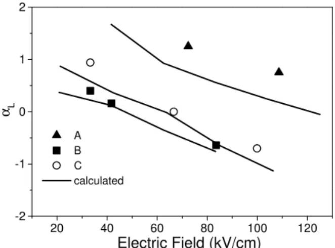
absorption curves, which are represented by solid lines in Fig. 2, well reproduce the experimental data represented by symbols. A –2V pre-bias and a detuning of 30 meV were used for both experimental and theoretical data.
20 40 60 80 100 120
-2 -1 0 1 2
A B C calculated
αL
Electric Field (kV/cm)
Figure 2. αLas a function of the externally applied electric field.
Solid lines and symbols areαLcalculated from the theoretical
ab-sorption curves and from the calibrated PC measurements, respec-tively.
The chirp parameter, for a QW alloy composition in the range from 0.494 to 0.502 and from 0.509 to 0.51, remains between 0 and –1 for applied reverse voltages between –1 and –5 V. These results are shown in Fig. 3.
0.47 0.48 0.49 0.50 0.51 0.52 0.53
-1 0
1 1 V
2 V 3 V 4 V 5 V
αL
x
Figure 3. Chirp parameter as a function of the Ga content for dif-ferent applied reverse bias.
694 Brazilian Journal of Physics, vol. 34, no. 2B, June, 2004
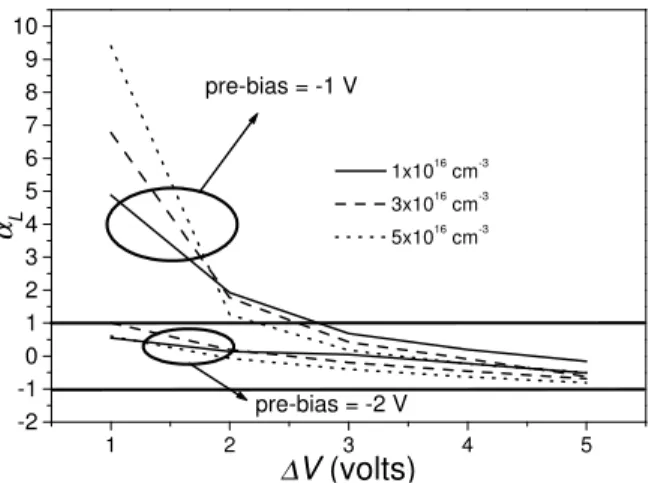
which gives 10 dB of contrast ratio (∆V10dB), increases
from 4.8 V to 5.6 V resulting from an increase of the RDL from 1 to 3x10¹⁶
cm−3. The value of 4.8 V can be recov-ered if instead of a pre-bias equal to –1V, a pre-bias of –2V is applied. Another result is that for low pre-bias,αL
de-pends very strongly on the RDL as shown in Fig. 4. This effect arises because since charge from background impuri-ties may affect the excitonic peak of the absorption curve, it may also affectαL. Such effect takes place for low pre-bias
because the MQW is not completely depleted. Suitable val-ues ofαLfor all applied voltages can be achieved only if the
value of the pre-bias is such that depletes the entire MQW region.
1 2 3 4 5
-2 -1 0 1 2 3 4 5 6 7 8 9 10
pre-bias = -2 V pre-bias = -1 V
1x1016 cm-3
3x1016 cm-3 5x10¹⁶
cm-3
αL
∆
V
(volts)
Figure 4.αLas a function of the applied reverse voltage for three
different values of the RDL. The first and the second sets of data were calculated respectively for –1V and –2V applied pre-bias. They are indicated by the circles and arrows.
5
Conclusion
Amplitude modulator parameters such as contrast ratio, chirp parameter and polarization sensitivity were considered theoretically. A good agreement between theoretical and ex-perimental values for the different parameters was obtained. The study of device parameters as a function of the MQW structure has shown that although minimum opera-tion voltage and polarizaopera-tion independence can be simulta-neously obtained, the correspondent αL is not optimized.
The influence of both RDL and applied pre-bias in the de-vice parameter was addressed.
Acknowledgement
This work has been partially supported by CNPq, FAPERJ and by the Research and Development Center, Er-icsson Telecomunicac¸˜oes S.A., Brasil.
References
[1] Y.-J. Chiu, H.-F. Chou, V. Kaman, P. Abraham, and J. E. Bowers, IEEE Photonics. Technol. Lett.14,792 (2002). [2] M. P. Pires, P. L. Souza, B. Yavich, R. Guerra, and W.
Car-valho, J. Lightwave Technol.18, 598 (2000).
[3] K. Yoshino, T. Takeshita, I. Kotaka, S. Kondo, Y. Noguchi, R. Iga, K. Wakita, and J. Lightwave Technol.17, 1700 (1999). [4] P. Voisin, Semicon. Sci. Technol.11, 1601 (1996).
[5] T. Yamanaka, K. Wakita, and K. Yokoyama, Appl. Phys. Lett.
68, 3114 (1996).
[6] M. K. Chin e W. S. C. Chang , IEEE J. Quantum Electron.