Spae-Charge-Limited Condution in Thin Film
Al/Sb
2 Pb
1 Se
7
/Al Devies
ShailaWagle and Vinay Shirodkar
SolidState EletronisLaboratory, DepartmentofPhysis,
TheInstituteof Siene,15,MadamCamaRoad,
Mumbai-400032. India
Reeivedon20June,1999. Revisedversionreeivedon10November1999
Thin lm Al/Sb2Pb1Se7/Al, MGM, sandwihed strutures, prepared using thermal evaporation
tehniquehavebeenstudied. TheDCmeasurementsatloweletrieldsuggestthattheeletrial
transportisgovernedbyspaehargelimitedondution(SCLC)mehanism. Thedetailedanalysis
of urrent-voltage limited ondution (SCLC) mehanism harateristis on the basis of SCLC
theory reveals thepresene of uniformlydistributed trap densityof the orderof 10 23
m 3
eV 1
withaverage ativationenergy0.48eV.
I Introdution
Thinlmtehnologyiswellestablishedandwidelyused
in thefabriating ofeletroni devies. Thetehnique
hasbeen suessfullyused to fabriate thin lm
resis-tors, apaitors, photoeletroni devies et.[1,2℄. The
use of this tehnique in fabriating eletroni devies
makesitneessarytounderstandtheeletrial
proper-tiesofthematerialin thinlmform.
In the devie appliations of thin lms, new and
omplex materials are being used and developed and
theireletrialpropertiesarebeingstudied. The
disor-dered materials. partiularly amorphous
semiondu-tors, overing a wide range of ompositions and with
interesting eletrial properties, have been studied in
greater detail[3-5℄. A good amount of work on the
DCondution ofhalogenide/glassymaterialsinthe
form of metal-glass-metal (MGM) struture has been
reported by many researhers[3,6℄. Sine these
mate-rialsare weilknownfor their property to swith from
oneimpedanestatetoanother,whensubjetedtohigh
eld of the order Of 10 6
V/m, most of the reported
work pertains to the eletrial measurements arried
outat highelds. However,itis equallyimportantto
know the behaviour of these materials at low eletri
eldsuptoabout10 4
V/m.
Tothebest ofourknowledgenoattempt hasbeen
madeto studytheloweld DCondution ofvauum
evaporated Sb
2 Pb
1 Se
7
thin lms. In the present
pa-pertherefore, wereport onthe loweld DC
measure-tionmehanisminvauumdepositedSb
2 Pb
1 Se
7 lms.
II Experimental
TheSb
2 Pb
1 Se
7
ompoundusedtofabriatethe
metal-glass-metal, MGM, devies was prepared as follows.
Initially,theweighedquantitiesofhighpurity(5N)Sb,
Pb and Se, taken in their atomi proportions, to give
Sb
2 Pb
1 Se
7
omposition, were rushed and mixed
to-gether. Themixturewasthenintroduedinahigh
pu-rityquartztubelosedatoneendandmadeintoanek
withonstritionattheotherend. Thequartzampoule
wasevauatedto 10 5
mbarandlledagain withdry
argontoinreaseitspressuretoabout10 3
mbar. The
ampoulewassealedatthepointofonstritionand
in-troduedinarokingfurnae. Thetemperatureofthe
furnae wasraisedto 1100 Æ
C and maintainedat that
levelforaboutvehours. Therokingfurnae helped
thoroughly to mix the onstituents in thequartz
am-pouleto form theompound. After ompletion of the
reationthequartzampoulewasallowedtofalldiretly
intoaliquidnitrogenontainer. Theampoulewasthen
brokeopenandglassymassthusobtainedwasrushed
into nepowderandstoredseurelyin adessiator.
The MGM devies were fabriated, on thoroughly
leaned mirosope glass slides, using Edwards Co.
(UK) Turbomoleular pumping station. The working
hamber was tted with Maxtek (USA) lm
deposi-tionontrollermodelFDC-440,whihandisplaylm
parame-and many suh parameters are fed into the program.
The thiknessof lm wasalso measuredusingDektek
thiknessprolometerand wasfound to be within 1%
ofthedisplayedvaluebytheFDC-440. Thebaseplate
housed aneightsoure turret,while thetopplate was
ttedwithmaskhangerassembly,bothofwhihould
bemonitoredexternallywithoutrequiringtobreakthe
vauum. Theultimateworkingpressureduringthe
de-positionwas510 6
mbar. Initially,aluminiummetal
wasevaporatedand deposited onthe substrate in the
form oftwoparallelstripseah60mmlong,2mm wide
and separated by5mm from eah other. These strips
formed a pair of lower eletrodes. The material was
deposited on the strips through an appropriate mask
to over area of 50mm 15mm, leaving 5mm of the
endportionsofeahaluminiumstrip. Sixounter
ele-trodes,eah2mm wideand20mmlong,perpendiular
to thelowereletrodesweredepositedonthe material
toobtain12MGMdevieseahofarea4mm 2
(seeFigs.
1a and 1b). The entiredeposition sequene was
om-pletedwithoutbreakingthevauumatanystage.This
madeitonvenientrepeatedlytoarryoutallthe
ele-trial measurementsonalm,ofanypartiular
thik-ness, using twelve devies prepared essentially under
idential deposition onditions.
Figure 1. a. Shemativiewof metal-glass-metal devies.
b. Crosssetionalviewofthedevies.
The eletrial measurements on the devies were
arriedoutin vauumusingaryostatwhihouldbe
evauatedto 10 2
mbar pressureduring the
measure-ments. The substratetemperatureinside theryostat
ould be varied from 150 K to 500 K. The
urrent-voltage, I-V, measurements were arried out using a
regulatedpowersupplyonnetedinserieswiththe
de-vie under investigation and astandard resistor. The
urrentthroughthedeviewasalulatedbyaurately
monitoringthepotentialdroparossthestandard
resis-voltage arossthe devie was obtainedasa dierene
between supply voltage and drop arossthe standard
resistor. The seriesresistoralso helpedto preventthe
ow ofexessiveurrentthroughthe devie when the
supplyvoltagewouldovershootaidentally.
III Results and disussion
Fig. 2,urve'a',showsatypialroomtemperatureI-V
urveof Al/Sb
2 Pb
1 Se
7
/AI sample with lm thikness
270nm. Itisseenthattheurveexhibitsahighly
non-linearfeature. Thenon-linearityoftheI-V
harateris-tisindiatesthattheprevalentondutionmehanism
isnon-ohmiinnature.
Figure2. RoomtemperatureI-V.urvea,andlogI V 1=2
,
urveb,harateristisofanMGMdevie withlm
thik-nesses270nm.
It wasobserved during themeasurementsthat the
reported I-V harateristis were reproduible when
ountereletrodewasbiasedwitheitherpolarity. This
indiatedthatthemetal-glassinterfaesatbottomand
topeletrodeswereidentialin nature.
The results shown in gure 2 need to be
are-fullyanalysed,toidentify thepredominantondution
mehanism,sinedierenttypesofondution
meha-nismsan give rise to non-linear harateristis. One
an rst explain observed non-linearity in terms of
Rihardson-Shottky[7℄orPoole-Frenkel[8℄typeof
on-dutionmehanisms. Shottkyemission ours due to
thermalativationofeletronsoverthemetal-insulator
or metal-semiondutor interfae barrier beause of
loweringofbarrierheightduetotheappliedeld. The
eletrons from traps into the ondution band of the
insulator. In boththeaseslog I vs. v 1=2
harateris-tisareexpetedto belinearin nature. InFig. 2the
urve'b',showslogIvs. v 1=2
harateristisofa
typi-alrepresentativesamplewithlmthikness270nm. It
is seenthat theharateristiurveisstill non- linear
in nature, whih rules out the possibility of existene
of Rihardson Shottky or Poole- Frenkel as possible
ondutionmehanisms.
Theother ondution mehanism,whih gives rise
toahighlynon-linearI-Vharateristis,isthe
spae-harge-limited ondution (SCLC)[9℄, whih is
inu-enedby the traps. However,the exatnature of the
traps presentin thematerial under study depends on
the type of the traps and their position with respet
to the Fermi-level. It is therefore, neessary to apply
this theory veryarefully to explain the experimental
results. In aseof SCLC proessthe detailed features
ofthe non-linearI -V harateristisarerevealed in
log I - log V plot. Fig. 3 shows logarithmi plot of
the I - V harateristis of the devies with dierent
lm thikneses. It is observed that, the urrent
ow-ing throughthe devie dereases with inreasein lm
thikness. However, the natures of theurvesremain
the same. It is seen that the harateristis are
dis-tributedinfourregions(markedAB,BC,CDandDE)
havingdierentslopes,whihimpliesthattheI-V
re-lationisofthetypeI /V n
wherenistheslopeofthe
urve.
Figure3. Log I -log V harateristisof thedevieswith
dierentlmthiknessesat294K.
For verylow voltages (i.e. urveAB) the slope is
equal to unity indiating that the ondution
meha-that in this regionthe urrent isdiretly proportional
totheappliedvoltage.
Intheregion2,urveBC,thevalueof exponentn
is found to be nearly equal to 2.5. This region starts
atapartiularvoltage,V
x
,whihistheendoftherst
region. Thus,atV
x
,theondutionmehanismisboth
OhmiandSCLC.ItisalsonotedfromtheFig. 3that
V
x
inreasesasthiknessinreases.
In the third region, urve CD, the slope inreases
to thevaluemuhlargerthan2. Thisregionisalmost
paralleltotheurrentaxis,indiatingthattheurrent
-voltagerelationfollowsamuh higherpowerlaw. The
transition voltage from seond region to the third
re-gionisdenoted byVTFL,whih inreasesasthikness
inreases.
In the region 4, urve DE, the exponent is again
foundtobe2,indiatingatraPlledSCLC proess.
It is also notied that the slopesof all the regions
areindependentoftheselmthikness.
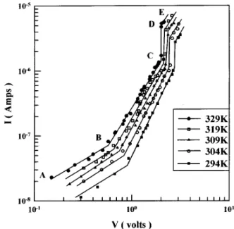
Fig. 4 shows the log I - log V harateristis at
ve dierent temperatures of a typial representative
sample of lm thikness 270 nm. It is seen that the
natureoftheurvesisessentiallysameasthat,in Fig.
3. It is also seen that as the temperature inreases
urrentthroughthedevieinreasesbutVxandVTFI
derease.
Figure 4. Log I -log Vharateristis ofthedevieswith
thikness270nmatdierenttemperatures.
Itisalsonotiedthattheslopesoftheurvesin
re-gionBCare temperaturedependentsuhthat as
tem-peratureinreasestheslopesdereaseslightly;but the
slopesofregionsAB,CDand DEarepratially
inde-pendentoftemperature.
sug-MGM devies under present study is governedby the
SCLC mehanism. Therefore, the results of the
mea-surementsonthedevieswithvariousglassthiknesses
andtemperaturesareanalysedonsimillarlinesandare
showntobeonsistentwiththeSCLCmehanism.
Sinevauumevaporatedlmstendtobeamixture
ofamorphousandrystallineregions,oneanexpeta
large onentration of traps distributed in the energy
band-gap [10℄. Therefore, the SCLC phenomenon
ap-propriatetosuhdistributionanbeappliedtodesribe
theondutionintheselms. Astheexatdistribution
oftrapsisdiÆulttopredit,anapproximationstothe
real distributionwasattempted.
TheFigs. 3and4showthattheI-Vharateristis
are governedby the relation I /V n
. Also the plot
showstwodistintross-overvoltages,V
x
representing
transition from Ohmi ondution to the SCLC with
traps, and the V
TFL
, whih is transition from SCLC
with traps to the trap lling level. This implies that
the traps, in the present ase, are situated at energy
levelhigherthanthatoftheFermi-levelofthematerial.
Hene traps are expeted to behave like donors [11℄.
Also, the temperature dependene of the region
sug-gestsapossibilityofexponentialdistributionoftraps.
Lampert hasshown [9℄that the urrent density in
theseondregionisgivenby,
J =
9
8
(K
0 )
V 2
S 3
(1)
where
J =urrentdensityintheseondregion
K =dieletrionstantofthematerial
0
=permittivityoffreespae
=ratiooffreehargearrierstothetrapped
ar-riers
S =thiknessof thelm
=mobilityofthearriers
V =applied bias
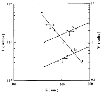
Eq. (1) suggeststhat to establishthe existeneof
SCLCaplotoflogIversuslogSshouldyieldastraight
linewithslopeequalto-3. Theurve'a'inFig. 5shows
logI-logSurvegeneratedusingdataofFig. 3
orre-spondingto aonstantvoltagebiasof 0.8V.Itis seen
Figure5. Curvea: Log I-log Sharateristisof the
de-vies.Curveb:LogVx-logSharateristisofthedevies.
Curve : Log VTFI- log S harateristis of the devies.
Temperatureofthedevie=294K.
The transition voltages, V
x and V
TFL
, transition
from Ohmi region to the ondution with tras and
transitionfrom ondution with traps to thetrapfree
ondutionrespetively,aregivenby,
V
x =
8
9
en
0
S 2
(2)
V
TFL =
eQ
TFL S
C =
eQ
TFL
AK
0
S 2
(3)
where
Q
TFL
=hargearriersinjeted atV
TFL
e=eletroni harge
C =apaitaneatV
TFL
A=areaofthedevie
n
0
=freearrierdensity
Eqs. 2and3suggestthattheplotsoflogV
x versus
logS and logV
TFL
versuslog S should yieldstraight
lineswith slope2. Fig. 5,urve'b'giveslog V
X - log
S urve, while urve '' gives log V
TFL
versus log S
plot. Theslopesoftheurvesbandarerespetively,
2.17and1.97whihprovideadditionalsupportforthe
existeneofSCL ondution.
Thetemperaturedependeneoftheurrentdensity,
J,in theseondregionisgivenby[11℄,
j=en
0 Fexp
F
0 K
eN
t kTS
(4)
where
F =eletrield= V
S
N
t
J
V =
en
0
S
exp
V
0 K
eN
t kTS
2
(5)
) J
V =A
0 exp
V
V
0
(6)
with
A
0 =
en
0
S
(7)
V
0 =
eN
t kTS
2
0 K
(8)
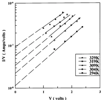
Thus, a plot of log (I=V) versus V should yield a
straightline with slope(1=V
0
) and intereptA
0 . Fig.
6showsthelog (I=V)versusV plots, generatedusmg
thedata of Fig. 3,for thesamples with dierentlm
thiknesses. Fig. 7 shows simillar plots, for various
temperaturesgeneratedusingdataofFig. 4. Itisseen
that, while the slopes of the urves in the Fig. 6
re-main thesame,they dereaseslightlywith inreasein
temperature, as revealed from Fig. 7. The derease
inslope(1=V
o
)withtemperatureimpliesthattheRose
model, [12℄ whih preditsthe natureof trap
distribu-tion anbe applied in the present ase. Using Eq. 7
and interepts of plots in Figs. 6 and 7, trap
densi-ties for various lm thiknesses and temperatures are
omputed. These values are shown in table 1a and
1b respetively. It It is seen that the trap densities
oftheorderof10 23
m 3
eV 1
exist forthepresent
sys-tem. These values are in lose agreement with those
reported for thesimillar disordermaterials.[13,14℄For
highly disorderedmaterialthemagnitude oftrap
den-sity isashigh as10 27
m 3
eV 1
hasbeenobservedfor
vauumdepositedCdSlms.[15℄
Figure6. Log(I/V)-V harateristisofthe devieswith
Figure 7. Log (I/V) - V harateristis of the devies at
dierenttemperatures,lmthikness=270nm.
Table1. Variationoftrapdensitywiththikness,
table(a), andtemperature,table(b).
(a)
Temperature=294K
Thikness N
t (m
3
eV 1
)
nm 10
23
150 6.299
108 4.374
204 3.405
230 2.679
270 1.944
(b)
Thikness=270nm
Temperature N
t (m
3
eV 1
)
K 10
23
294 1.944
304 1.640
309 1.347
319 1.172
329 1.055
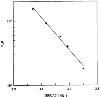
Itisfurther seenthat usingequation 7and the
in-tereptsthevaluesforn
0
anbealulatedfrom the
interepts. The interept, log A
0
, is also found to be
a funtion of the mobility of arriers, free eletron
density andthe thiknessof thedevie. Themobility
=
0 exp
E
t
kT
(9)
where E
t
istheativationenergyofthetraps
Eq. (9)anberewrittenas
n
0 =n
0
0 exp
E
t
kT
(10)
Thus,itispossibletoextratinformationaboutthe
a-tivation energyofthetraps byplottinglog n
0
versus
1/T(Fig. 8). Itisseenthattheplotislinearand,from
the slope, the value of E
t
is alulated to be 0.48eV,
whihistheativationenergyoftraps. Thisvalueisin
loseagreementwiththereportedoneforsimillartype
ofhalogenidematerials[17℄.
Figure 8. Log (n0) -(1/T) harateristis of the devie
withlmthikness270nm.
The distribution of the traps in the devie ould
be either disrete or exponential. Rose [12℄ gives the
urrent voltage relation, whih is in the form I /
V
[(T=T)+1℄
,whereTistheharateristitemperature.
Thus [(T=T)+1℄ isthe slopeof theseond regionof
Fig. 3 whih givesT as 600K. Thus, kT beomes
0.05eV,whihisverysmallomparedtotheaverage
a-tivationenergyofthetrapsdeterminedas0.48eV.This
suggeststhatthedistributionoftrapsisuniformwhih
isexpetedforamorphousorpolyrystallinelms[12℄
IV Conlusions
InthispaperloweldDC harateristisof theMGM
deviesareanalysed. Thedominantondution
meha-nismisidentiedasSCLCproess. Itisfurthershowed
thatthe traps aredistributed uniformly in the
forbid-den band-gap. The ativation energy of the traps is
estimatedas0.48eV. Thetrapdensityisfoundto
de-rease for inrease in both the lm thikness and the
temperature.
Aknowledgement
The authors wish to thank Prof A.P. Sathe, for
stimulating disussions and for ritially reading the
manusript.
Referenes
[1℄ L. Kasturi, Thin Film Phenomena, Mgraw-Hill Book
Company.
[2℄ N.F.Mott andE.A. Davis, Eletroni Proess In
Non-rystallineMaterials,ClarendonPress,Oxford2nd
edi-tion(1978).
[3℄ G.S. Nadkarni and V.S. Shirodkar, Thin Solid Films
105,115(1983).
[4℄ V.K. Dhavan, A. Mansingh and M. Sayer, J.
Non-rystallineSolids51,87(1982).
[5℄ K.NassauandD.W.Murphy,J.Non-rystallineSolids
44,297(1981).
[6℄ A.ServiniandA.K.Jonsher,Thin SolidFilms3,341
(1965).
[7℄ W.Z.Shottky,Phys.15,872(1914).
[8℄ Frenkel,J.Phys.Rev.54,647(1938).
[9℄ M.A. Lampert, RCA Teh. Report No. PTR., p 1445
(1963).
[10℄ J.G.Simmon,J.Phys.D4,613(1971).
[11℄ M.A. Lampert and P. Mark, Current injetions in
solids,NY.Lond.(1970).
[12℄ A.Rose,Phys.Rev.97,1538(1955).
[13℄ S.P.BodhaneandV.S.Shirodkar,J.Apply.Poly.Si.
Inpress(Publiationno.6700).
[14℄ T.Budinas,P.Makus,A. Smilga,J.Vivvakas,Phys.
Sol.Stat.31,375(1969).
[15℄ J.DresnerandF.V.Shallross,Sol.Stat.Eletr.5,205
(1962).
[16℄ I. Solomon, R. Benferhat and H. Tran-Quo, Phys.
Rev.B30,3422 (1984).
[17℄ N.KenshiroandC.K.KwanJpn.Appl.Phys.18,1161