Bachelor in Micro and Nanotechnologies Engineering Sciences
Development of Plasmonic Nanosandwiches
for Biosensing Applications
André de Távora Vasconcelos de Moura
Examination Committee
Chairperson: Dr. Hugo Manuel Brito Águas
Rapporteur: Dr. Manuel João de Moura Dias Mendes
Member: Dr. Elvira Maria Correia Fortunato
Supervisor:
Duncan Sutherland, Professor, iNANO,
Aarhus Universitet
Co-supervisor:
Elvira Fortunato, Full Professor, Faculdade
de Ciências e Tecnologias, Universidade
Nova de Lisboa
Dissertation submitted in partial fulfilment of
the requirements for the degree of
Master’s in
Engineering of Micro and
Nanotechnologies
iii
Development of Plasmonic Nanosandwiches for Biosensing Applications
Copyright © André de Távora Vasconcelos de Moura, Faculdade de Ciências e Tecnologia, Universidade Nova
de Lisboa.
A Faculdade de Ciências e Tecnologia e a Universidade Nova de Lisboa têm o direito, perpétuo e sem limites
geográficos, de arquivar e publicar esta dissertação através de exemplares impressos reproduzidos em papel ou
de forma digital, ou por qualquer outro meio conhecido ou que venha a ser inventado, e de a divulgar através
de repositórios científicos e de admitir a sua cópia e distribuição com objetivos educacionais ou de investigação,
v
“
No
one should be ashamed to admit they’re
wrong, which is but saying, in other words, that
they are wiser today than they were yesterday.
”
vii
Acknowledgements
First of all, I want to thank to my supervisor Professor Duncan Sutherland for answering my first email and allowing me to develop this work in Denmark. For about 6 months I lived in a foreign country and met amazing people there, all thanks to a simple, random email reply. I would also like to thank for all the feedback given about what should I do and all I learnt in the meantime, all the meetings, coffees and the late Christmas dinner and some comforting words when things weren’t going so well. Then, I’d like
to thank 马睿 (Mǎ Ruì) for showing me what is the basic methodology used both in the lab and in the
cleanroom and most importantly for the FDTD simulations included in this report. Finally, to the rest of Nanobiointerfaces group (Hans, Pita, Heba, Hossein, Gunnar and Christina) for making me feel welcome at iNANO.
I’d also like to thank to Professor Elvira Fortunato for being the link between Denmark and Portugal, and for having accepted to be my supervisor. Thank you for all the opportunities and challenges offered in this course that you helped create and develop.
Having this thesis being made abroad, I couldn’t fail to thank everyone I met there. Starting from the Portuguese group I met in Danish lands, thanks for the barbecues, meet ups and specially the distance shortening from home, being able to speak Portuguese for a change. Also, and not the least important, I’d like to thank Carlos, Pol, Marek, Erika, Gabriela, Gonzalo, Luis, Romana, Álvaro, Melissa, Guillaume, Rikke (and to all I forgot to mention) for the Wednesday Kushtall nights, Friday Bars and other things we did together. I can honestly say I met amazing people whom I won’t forget. Tusinde tak for alt!
On a general note, to my all my friends who have had to put up with me all this time. My course colleagues, for making this 5-year journey with me. To the ones with who I made almost every group project since the beginning (Miguel) and those with who I just started to appreciate the company mid-way (Marta Pereira and Recife). To Tibério for being a decent ‘praxe’ godson and Pipa for being a pseudo-goddaughter. To Carolina for being someone I can count on even if we lost some contact by the end.
Now to my long-time friends (high school, primary school or even before that), with whom I go to the ‘sede’ just to hang out in silence, or play ‘sueca’. Rodra, Zé Luís, Brás and Diogo (Marta Ribeiro de Sousa, Madalena, Faria and Mónica who joined this group later), I can fortunately say I know we will be friends until the end and I know I can count on you for almost everything. The same I can say to other friends (Manô, Celso and Marta Aguiar), even if I don’t see you as regularly as the other group. Thanks for listening to me, for talking to me when I needed and all the (mostly) good and bad times. Also, a word of appreciation to Luísa, Inês and Kika as you have also been part of pretty much all my life, having spent so many vacations together. I want to leave a word of appreciation to the ones I consider a friend and acquaintance even if I don’t mention them here. You were also important in one way or another to me, even if it was for my personal growth.
ix
Resumo
Foram estudadas estruturas compostas por dois discos de ouro de diâmetros diferentes, separadas por uma camada fina de alumina, para biodeteção de proteínas. O disco superior será menor, uma vez que tem um comprimento de decaimento mais curto (e como tal, maior sensibilidade), enquanto que o disco inferior de maior dimensão irá dar um sinal de alta intensidade devido à sua maior interação com a luz. A interação entre os dois discos acontecerá através da hibridização plasmónica. A caracterização das amostras consistiu na análise morfológica por microscopia eletrónica de varrimento (SEM), a resposta ótica foi estudada experimentalmente e por simulações de domínio do tempo de diferença finita (FDTD) e também analisada a distribuição do campo elétrico em três tipos de estrutura. Foram estudadas estruturas com o disco superior numa posição central relativamente ao disco inferior tal como na extremidade do mesmo, e também o efeito da espessura do óxido (3 e 6 nm). O pico de baixa energia é sobretudo devido a um modo plasmónico dipolar na separação dos discos metálicos, enquanto que o pico de alta energia é dado pela contribuição do modo da separação e pelo dipolo resultante da estrutura. A estrutura com menor separação e com o disco centrado em relação ao disco inferior tem um aumento do campo elétrico em redor da mesma maior e deverá ser esta a utilizada como biossensor.
Palavras chave: Biossensor, ressonância plasmónica de superfície localizada, hibridização
xi
Abstract
Structures composed of two gold disks with different diameters and separated by a thin alumina layer were studied for protein biodetection. The small top disk will be used as the biosensing element since it has a shorter decay length (and thus, it has a higher sensitivity) whereas the big bottom one will give a high signal due to its bigger interaction with light. The interaction between both disks will happen through plasmon hybridisation. The samples were prepared using colloidal lithography and material deposition was made through an electron beam assisted evaporation system. A fabrication method was developed to spatially isolate the bottom disk from the sensing medium to fully exploit the small disk’s higher sensitivity. Sample’s characterisation consisted in a morphologic analysis by scanning electronic microscopy (SEM), the optical response was studied experimentally and by finite-domain time-difference (FDTD) simulations and also the electric field distribution was analysed in three types of structures. Structures with the upper disk centred relative to the lower disk and at the edge of it. The oxide’s thickness effect was studied (3 and 6 nm). The low energy peak is mainly given by a plasmonic gap dipole mode, whereas as the high energy peak is given by a contribution from a gap mode and the structure’s overall net dipole. The structure with a smaller separation and the top disk centre regarding the bottom disk was found to have a higher electric field enhancement around it and should be the one to be used as a biosensor.
Keywords: Biosensor, localised surface plasmonic resonance, plasmon hybridisation,
xiii
Contents
1.
MOTIVATION AND OBJECTIVES
1
2.
INTRODUCTION
3
2.1.
PLASMONICS
3
2.1.1. L
OCALISEDS
URFACEP
LASMONICR
ESONANCE3
2.1.2. P
LASMONC
OUPLING INC
LOSELYL
OCATEDP
ARTICLES5
2.1.3. S
URFACEP
LASMONP
OLARITONS ANDG
APM
ODES5
2.2.
NANOFABRICATION
5
2.2.1. H
OLE-M
ASKC
OLLOIDALL
ITHOGRAPHY6
3.
MATERIALS AND METHODS
9
3.1.
NANOSTRUCTURES FABRICATION
9
3.1.1. S
UBSTRATEC
LEANING9
3.1.2. S
ACRIFICIALL
AYERS
PIN-
COATING9
3.1.3. P
OLYELECTROLYTEL
AYER ANDP
OLYSTYRENEP
ARTICLESD
EPOSITION10
3.1.4. M
ETALD
EPOSITIONS10
3.1.5. S
AMPLESD
EVELOPMENT11
3.1.6. Q
UARTZS
AMPLESE
TCHING11
3.1.7. O
XYGENP
LASMAT
REATMENTS11
3.2.
SAMPLES CHARACTERISATION
11
3.2.1. S
CANNINGE
LECTRONM
ICROSCOPY11
3.2.2. E
XTINCTIONM
EASUREMENTS11
3.2.3. FDTD
S
IMULATIONS11
4.
RESULTS AND DISCUSSION
13
4.1.
FABRICATION STEPS
13
4.2.
EXTINCTION MEASUREMENTS
–
EXPERIMENTAL AND SIMULATIONS17
4.3.
FDTD FIELD PLOTS
20
5.
CONCLUSIONS AND FUTURE PERSPECTIVES
25
6.
REFERENCES
27
7.
ANNEXES
29
7.1.
ANNEXE A
–
IMAGEJ PROCESSING29
7.2.
ANNEXE B
–
MATLAB CODE33
7.2.1. F
UNCTIONP
ARTICLED
ISTANCE33
7.2.2. F
UNCTIONM
ATCH34
7.2.3. F
UNCTIONN
OTM
ATCH35
xv
List of Figures
FIGURE 1.1–A)CROSS SECTION OF THE IDEAL STRUCTURES TO BE DEVELOPED.B)CROSS SECTION OF THE STRUCUTRES WITH PROTEINS
(IN BLUE) TO BE DETECTED BOUND ONLY TO THE UPPER DISK. ... 2
FIGURE 2.1-DIPOLE 𝑝⃗ CREATED ON A SPHERICAL METAL NANOPARTICLE DUE TO THE INCIDENT LIGHT WITH A WAVELENGTH SUCH THAT IS LONGER THAN THE PARTICLES’ SIZE. ... 4 FIGURE 2.2-REPRESENTATION OF THE ELECTRIC FIELD (IN THE FORM OF FIELD LINES) CREATED DUE TO THE ELECTRONS’ MOVEMENT TO
THE PARTICLE’S SURFACE WHEN EXCITED BY LIGHT.ADAPTED FROM 27. ... 4 FIGURE 2.3-SCHEMATIC OF THE HOLE-MASK COLLOIDAL LITHOGRAPHY PROCESS.ON THE BOTTOM OF THE FIGURE, IT IS SHOWN SOME
POSSIBLE STRUCTURES FABRICATED WITH THIS METHOD, BEING THE STANDART DISKS, WHILE VARYING THE THICKNESS OF MATERIAL CAN RESULT IN CONES, AND VARYING THE DEPOSITION ANGLE IN METALLIC DIMERS.REPRODUCED FROM 23. ... 7 FIGURE 3.1–GENERAL SCHEMATIC OF THE NANOSANDWICHES FABRICATION, STARTING WITH CLEAN SUBSTRATES.THE INCLUDED
STEPS ARE:1–PMMA SPIN-COATING;2–POLYELECTROLYTE LAYER AND POLYSTYRENE PARTICLES DEPOSITION;3–ETCH MASK DEPOSITION;4–PARTICLES TAPE STRIPPING;5–PMMA ETCHING;6–AU AND AL LAYER DEPOSITION, FOLLOWED BY AL OXIDATION;7–HOLE SHRINKING USING AN OBLIQUE DEPOSITION;8–SECOND AU LAYER DEPOSITION AT A)0° AND B)6°;9 LIFT-OFF.THE QUARTZ SAMPLES ALSO INCLUDED AN EXTRA SUBSTRATE ETCHING STEP (E). ... 9 FIGURE 4.1-SCHEMATIC CROSS-SECTION OF THE FINAL STRUCTURE.A THIN LAYER (3 NM) OF AL2O3(IN GREY) SANDWICHED BY A BIG
(120 NM DIAMETRE) BOTTOM AU DISK AND A SMALL (55 NM DIAMETRE)AU SMALL DISK, BOTH HAVING A 20 NM HEIGTH (BOTH IN ORANGE). ... 13 FIGURE 4.2–140 NM PSNPS SPREAD OVER A PMMA SURFACE WITH TWO DIFFERENT MAGNIFICATIONS, AT A)10K TIMES AND B)
50K TIMES.THESE IMAGES WERE OBTAINED ON A SILICON SUBTRATE AND A LOWER VOLTAGE (2.5 KV) AND NOMINAL CURRENT
(25 PA) TO AVOID CHARGING AS MUCH AS POSSIBLE. ... 13 FIGURE 4.3-TITANIUM MASK USED DURING THE FABRICATION PROCESS A) BEFORE AND B) AFTER THE EXTRA TITANIUM LAYERS
DEPOSITION.B) SHOWS ALSO SOME PSNPS WHICH WERE NOT TAPE-STRIPPED AND SOME AGGREGATION.THESE SAMPLES WERE NOT COVERED IN TI SINCE THE MASK IS ALREADY A CONDUCTIVE LAYER.THE BLUE CIRCLES IN BOTH SIDES REPRESENT A 200 NM DIAMETRE CIRCLE IN THE RESPECTIVE SCALES. ... 14 FIGURE 4.4–SEM PICTURE OF THE FINAL STRUCTURES AFTER REMOVING THE SACRIFICIAL LAYER WITH ACETONE WITH THE TOP DISK
DEPOSITED AT A)0° AND B)6°.ALMOST EVERY DISK PAIR HAS APPROXIMATELY THE SAME DIAMETER.HOWEVER, IN A), A FEW MAY BE OF A DIFFERENT SIZE, LIKE THE ONES MARKED IN RED.IN B), MARKED IN GREEN ARE SOME DEFECTIVE STRUCTURES. .... 14 FIGURE 4.5-SCHEMATIC OF THE SMALL DISK FABRICATION.THE MATERIALS USED ARE THE SAME EXCEPT THE BOTTOM DISK, WHICH IS
3.9 NM HIGH SIO2(DEPICTED IN BLACK) INSTEAD OF AU. ... 15 FIGURE 4.6–SEM IMAGE OF SMALL DISKS ON THEIR OWN, USING A SIO2 LAYER TO REPLACE THE BIG AU DISK. ... 15 FIGURE 4.7–SEM PICTURES OF A) ETCHED HOLES ON QUARTZ AND B) ETCHED HOLES FILLED WITH GOLD OF 20 NM HEIGHT, ALSO ON QUARTZ.BOTH PICTURES WERE TAKEN WITH THE SAMPLE TILTED AT 50°. ... 16 FIGURE 4.8–TWO NANOSANDWHICH STRUCUTRES INSIDE A HOLE MADE ON THE QUARTZ SUBSTRATE.THE SAMPLES WERE TILTED AT
57°. ... 17 FIGURE 4.9–EXTINCTION SPECTRA FOR INDIVIDUAL DISKS, BIG (IN BLACK) WITH A DIAMETRE OF 118 NM AND SMALL (IN RED) WITH A
DIAMETRE OF 69 NM.IT IS POSSIBLE TO SEE A DIFFERENCE IN THE PEAK POSITION AS WELL AS EXTINCTION INTENSITY.THERE IS AN ADDITIONAL ARTIFACT ON THE BLACK LINE AT AROUND 1400 NM THAT ALSO SHOWED UP IN OTHER SAMPLES MADE AT THE SAME TIME, POSSIBLY DUE TO SOME HUMIDITY ON THE EQUIPMENT, SO IT SHOULD ALSO BE IGNORED. ... 17 FIGURE 4.10–A)EXPERIMENTAL EXTINCTION SPECTRA FOR FULL STRUCTURES AND B) SIMULATED TRANSMISSION SPECTRA FOR THE
THE SAME STRUCTURES.IN BOTH, THE BLACK LINE CORRESPONDS TO THE TOP DISK CENTRERED WITH RESPECT TO THE BOTTOM ONE AND THE RED CORRESPONDS TO THE OFFSET DISK, PLACED AT THE EDGE. ... 18 FIGURE 4.11-A)EXPERIMENTAL EXTINCTION SPECTRA FOR FULL STRUCTURES AND B) SIMULATED TRANSMISSION SPECTRA FOR THE
THE SAME STRUCTURES.IN BOTH, THE BLACK LINE CORRESPONDS TO A DISK SEPARATION BY AL2O3 OF 3 NM AND THE RED LINE TO A DISK SEPARATION OF 6 NM. ... 20 FIGURE 4.12–Z-COMPONENT ELECTRIC FIELD PLOTS OBTAINED FOR THE RESPECTIVE LOW ENERGY PEAK WAVELENGTH OF THE A) AND
B) OFFSET STRUCTURE WITH 3 NM SPACER,C) AND D) CENTERED STRUCTURE WITH 3 NM SPACER AND A) AND B) CENTRED STRUCTURE WITH 6 NM SPACER.A),C) AND E) ARE OBTAINED FROM THE BOTTOM DISK/ALUMINA INTERFACE WHILE B),D) AND
F) IS A CROSS-SECTION THAT GOES THROUGH THE CENTRE OF THE TOP DISK.THE DASHED LINES REPRESENT THE PERIMETER OF THE DIFFERENT COMPONENTS OF THE STRUCTURE. ... 21 FIGURE 4.13–Z-COMPONENT ELECTRIC FIELD PLOTS OBTAINED FOR THE RESPECTIVE HIGH ENERGY PEAK WAVELENGTH OF THE A) AND
Development of Plasmonic Nanosandwiches for Biosensing Applications
xvi
F) IS A CROSS-SECTION THAT GOES THROUGH THE CENTRE OF THE TOP DISK.THE DASHED LINES REPRESENT THE PERIMETER OF THE DIFFERENT COMPONENTS OF THE STRUCTURE. ... 22 FIGURE 7.1-STARTING SEM PICTURE FOR IMAGEJ ANALYSIS.IT HAS SOME MARKS ON SOME PARTICLES AT THE EDGE (NEAR THE
INFORMATION BAR) TO FURTHER EXCLUDE THEM ON THE ANALYSIS. ... 29 FIGURE 7.2–‘THRESHOLD’ SUB-MENU.THE HISTOGRAM REPRESENTS THE ‘COLOUR’ DISTRIBUTION BY BIT NUMBER (FROM 0 TO 255)
OF THE PICTURE AND THE PIXELS WITH THE 'COLOUR' NUMBER BETWEEN THE RANGE (IN THIS CASE,63 AND 169) WILL TURN BLACK WHILE THE REST WILL TURN WHITE. ... 29 FIGURE 7.3–BINARY PICTURES OBTAINED FROM FIGURE 7.1 FOR A) BIG PARTICLES AND B) SMALL PARTICLES. ... 30 FIGURE 7.4–‘ANALYZE PARTICLES’ SUB-MENU.THE ISLANDS’ SIZE CAN BE DEFINED TO IGNORE SOME RANDOM PIXELS WHICH COULD
NOT BE EXCLUDED WITH THRESHOLD SELECTION. ... 30 FIGURE 7.5-OUTLINE PICTURES OBTAINED FROM FIGURE 7.3 FOR A) BIG PARTICLES AND B) SMALL PARTICLES.NOTE THAT EVERY
PARTICLE HAS A NUMBER AND THIS NUMBER IS ASSOCIATED WITH A SET OF MEASURES REGARDING TO THAT PARTICLE IN A SEPARATE .TXT FILE. ... 31 FIGURE 7.6- Z-COMPONENT ELECTRIC FIELD PLOTS OBTAINED (IN LOGARITHMIC SCALE) FOR THE RESPECTIVE LOW ENERGY PEAK
WAVELENGTH OF THE A) AND B) OFFSET STRUCTURE WITH 3 NM SPACER,C) AND D) CENTERED STRUCTURE WITH 3 NM SPACER AND A) AND B) CENTRED STRUCTURE WITH 6 NM SPACER.A),C) AND E) ARE OBTAINED FROM THE BOTTOM DISK/ALUMINA INTERFACE WHILE B),D) AND F) IS A CROSS-SECTION THAT GOES THROUGH THE CENTRE OF THE TOP DISK.THE DASHED LINES REPRESENT THE PERIMETER OF THE DIFFERENT COMPONENTS OF THE STRUCTURE. ... 37 FIGURE 7.7- Z-COMPONENT ELECTRIC FIELD PLOTS OBTAINED (IN LOGARITHMIC SCALE) FOR THE RESPECTIVE HIGH ENERGY PEAK
xvii
List of Tables
xix
List of Abbreviations
FDTD Finite-difference time-domain HE High energy
LE Low energy
LSPR Localised surface plasmon resonance PAX Polyammonium chloride
PDDA Poly(diallydimethylamminium chloride) PMMA Poly(methyl methacrylate)
PSNP Polystyrene nanoparticle PSS Poly(sodium-4-styrnesulfonate) SEM Scanning electron microscopy SPP Surface plasmon polariton UV Ultraviolet
xxi
List of Symbols
𝑬⃗⃗⃗ Electric field
𝒑⃗⃗⃗ Dipole moment
° Degree
°C Degree Celsius
Å Ångstrom
Al Aluminium
Al2O3 Alumina
Au Gold
cm Centimetre
i Imaginary unit
kV Kilovolt
me Effective electron mass
min Minute
mm Milimetre mTorr Millitorr
N Density of free electrons
N2 Nitrogen
nm Nanometre
O2 Oxygen
pA Picoampere
q Elementary charge
rpm Rotations per minute
s Second
sccm Standard cubic centimetre per minute SiO2 Silica
Ti Titanium
W Watt
γ Electron collision frequency ε Dielectric function
ε0 Dielectric permittivity
1
1.
Motivation and Objectives
Metallic nanostructures have been widely studied due to their interesting optical response, effectively enhancing the electric field near the structure’s surface. Many structures have been studied from simple nanospheres1, nanorings2 or nanodisks3–5. It is possible to include dielectric materials in the fabrication
process to make more complex structures as nanoshells6, nanocups7 or nanosandwiches8–10, usually
rendering two metallic structures physically separated, making a metal-insulator-metal configuration. This configuration has an additional field enhancement and confinement11 which could lead to interesting
developments. Some of the applications of this field confinement relate to waveguiding materials12,
photovoltaic devices13,14, development of metamaterials15,16 and sensitive biosensing5,17.
As far as metallic nanoparticle-based biosensors go, they can be used with different physical principles. For instance, gold is a highly conductive metal with catalytic properties, being suitable for electrochemical sensing18. It is also common to use such particles for signal amplification as generally,
some of them exist in low concentration in body fluids, for instance19. Other sensors rely on fluorescence.
Extremely small particles, called nanoclusters (up to 100 gold atoms18), have fluorescent properties due
to their size, as they behave like individual molecules. Compared to other fluorescent materials, these nanoclusters show high photostability and biocompatibility18,20.
Localised surface plasmon resonance-based biosensors are also a viable approach. This resonance happens at different light wavelength according to the metallic nanoparticle’s size, shape, surrounding
environment, amongst other factors18. The readout of such biosensors is based on a peak shift when
the desired protein2 or cell21 is located and bound to the structures, making the surrounding
environment’s refractive index different. They can reach sensitivities of around 1500 nm/refractive index unit, using a metal-insulator-metal configuration22.
This work intends to develop a series of nanostructures all over a substrate’s surface using a well-established nanofabrication method23. Each structure comprises two stacked metal disks, spatially
separated by a thin insulator layer. The top disk will act as the analyte sensor as it has a smaller diameter compared to the bottom one to be more sensitive in the presence of one molecule. The higher sensitivity arises from the shorter decay length that localised surface plasmon resonances have compared to the propagating surface plasmon resonances. The same would happen when comparing two nanoparticles with one dimension (diameter in this case) shorter than the other’s diameter, the former will have a shorter decay length24. The bottom, big disk will serve as an antenna to help produce a high, measurable
Development of Plasmonic Nanosandwiches for Biosensing Applications
2
3
2.
Introduction
2.1.
Plasmonics
Extensive research has been made in the past years on metal nanoparticles and their unique optical properties, as well as the interaction between two particles that are a few nanometres apart from each other3,4,7,8. Metals are shiny and reflective to the human eye because the frequency of the incident light
can be matched by the material’s free electrons’ oscillations, thus creating a screening effect that does not allow the wave to propagate through the material16. However, for light above specific frequencies,
the free electrons in the metal are unable to oscillate according to the frequency of the incident light, allowing light to propagate through the material at high frequencies. This plasma model does not take into account the interband transitions that happens in the visible frequencies in noble metals, limiting this approach to these frequencies11.
The frequency at which such propagation occurs is designated as bulk plasma frequency, 𝜔P, and it is given by25:
𝜔P= √𝑁𝑞 2 𝜀0𝑚e
(1)
Where N is the density of the free electrons in the metal, q the elemental charge, ε0 the dielectric permittivity and me the electron effective mass. Another result of this ability of the electrons to oscillate
accordingly to an external electric field is the variability of the dielectric function 𝜀(𝜔), described by Drude model (only considering the free electronic response) with a high frequency part (𝜀∞) due to the bound electrons for noble metals25:
𝜀(𝜔) = 𝜀∞−𝜔2𝜔+ 𝑖𝛾𝜔P2 (2)
where 𝛾 is the electron collision frequency (around 100 THz at room temperature11) and quantifies the
oscillation damping. The real part of a metal’s dielectric function for frequencies below 𝜔P is negative, meaning that the material will act as a conductive material11.
2.1.1. Localised Surface Plasmonic Resonance
When dealing with nanometric particles, there will be another influence from the nanoparticles’ surface that should be taken into account. Considering a simple nanosphere, a time dependent electric field interacts with the nanoparticle, in a way that makes the conduction electrons oscillate collectively accordingly to the incident light. As the electrons go away from their natural position, the atoms’ nuclei will exert an electrostatic attraction on the electrons, leading to a resonance. This resonance results in a field enhancement just outside the particle (near-field). Since these oscillations do not propagate, this
phenomenon is called localised surface plasmonic resonance (LSRP).11
Development of Plasmonic Nanosandwiches for Biosensing Applications
4
this happens, all the electrons will move accordingly to the nanoparticle’s surface, leaving a net positive charge on the other side, creating a dipole. This dipole will depend on the nanoparticles’ polarisability,
𝛼. This term reflects the electrons’ tendency to displace when excited with an external electric field and creating the dipole, which is given by11:
𝛼 = 4𝜋𝑎3 𝜀 − 𝜀𝑚
𝜀 + 2𝜀𝑚 (3)
Being 𝑎 the radius of the nanosphere, 𝜀 the dielectric function of the nanoparticle and 𝜀𝑚 the dielectric constant of the surrounding medium. Keeping in mind that the dielectric function of the metal varies with the incident light frequency, the polarisability can get a maximum value and thus, resulting in a resonance enhancement when the denominator reaches a minimum (Re[𝜀(𝜔)] = −2𝜀𝑚)11. So, it is
possible to understand that there is a frequency for which the dielectric function of the metal is such that fulfils this condition, and a LSPR is obtained.
Figure 2.1 - Dipole 𝑝⃗ created on a spherical metal nanoparticle due to the incident light with a wavelength such that is longer than the particles’ size.
When a LSPR is excited, a dipole is created, and this induces an electric field on the nanoparticle’s
surroundings (Figure 2.2). Near the particle’s edge, the accumulated charges on one end, alongside
with the absence of charges in the other, will create an electric-field enhancement4,26, where the
magnitude of this near-field at the surface is given by25:
𝐸𝑠𝑢𝑟𝑓𝑎𝑐𝑒=𝜀 + 2𝜀𝑚3𝜀𝑚 𝐸0 (4)
where E0 is the magnitude of the incident light’s electric field.
Figure 2.2 - Representation of the electric field (in the form of field lines) created due to the electrons’ movement to the particle’s surface when excited by light. Adapted from 27.
Another consequence of this LSPR is the scattering and absorption enhancement that also occurs. The plasmons can decay radiatively (leading to a far-field scattering) or not (leading to absorption)4.
5
reflects on the extinction spectra of a nanostructure. At the resonance frequency, the spectra shows a high intensity peak11,29 and these measurements are then representative of the plasmon oscillations and
the field enhancement25.
Although equations (3) and (4) apply only for spherical nanoparticles, the same phenomena occur on other shaped particles. There should be a correction on the polarisation since it differs for each direction as the electrons could have more space to oscillate along one direction compared to another11.
A disk, for example, can be considered as a flat ellipsoid, and will have different resonance frequencies should it be excited perpendicularly to the flat surface or parallel to it.
2.1.2. Plasmon Coupling in Closely Located Particles
When a metal nanoparticle is excited with light at a certain frequency, the near-field is enhanced. In case two separate nanoparticles are in close proximity, both near-fields can interact with each other and enhance it even more25. Two metal nanoparticle structures can be fabricated with the particles being on
the same plane3–5,23 or as a stacked structure using an insulator layer to separate them8,30. This last one
refers to metal-insulator-metal nanosandwiches, but other type of geometries using this kind of separation can be achieved6,7,31. The electrons’ oscillations of the two particles become coupled. A good
example of this is when spherical gold nanoparticles in solution aggregate, the extinction spectra red-shifts25,28.
In 2003, Prodan and his colleagues developed a model that could explain the plasmonic response for complex shaped nanostructures similar to the hybridisation that occurs in molecular orbital theory6.
They have studied how could a nanoshell response be understood as a combination or hybridisation of two simpler structures, a nanosphere and a nanovoid. The ‘individual’ plasmons of both sphere and void will interact with each other since there is a finite metal thickness and will result in a lower energy symmetric plasmon and a higher energy antisymmetric plasmon. Following this work, this model was successfully applied to metal dimers to determine the system’s resonance frequencies31.
2.1.3. Surface Plasmon Polaritons and Gap Modes
When there is a flat interface between a dielectric and a metal, surface plasmon polaritons (SPPs) can arise. These are electromagnetic excitations that propagate along the interface and the magnitude of the electric field decays evanescently perpendicularly to the interface. Should there be two insulator interfaces with a distance between them smaller than the SPP’s decay length (in a metal-insulator-metal structure, being the insulator a thin film of a few nanometres), both interfaces’ SPPs can interact with each other11, leading to plasmonic gap modes. An interesting result of this phenomenon is
the strong confinement of the electromagnetic field inside the insulator layer.
2.2.
Nanofabrication
Development of Plasmonic Nanosandwiches for Biosensing Applications
6
Bottom-up fabrication techniques are based on the assembly of small building blocks to achieve the desired structure, the same way as one would build a house by assembling bricks as desired. However, since it is not possible to pick an atom or molecule and place it wherever we want, there must be another way of doing this. Self-assembled monolayers are one type of structures built this way. It is a technique that allows to make a thin film of a certain material onto a surface as the molecules spatially arrange themselves spontaneously to form such structure, reaching the energetic equilibrium32. Sulphur has a
great affinity with transition metal surfaces in general (especially with gold). This interaction with gold is one of the most studied, and more specifically, alkanethiolates on gold. The sulphur head of these molecules can attach to the metal’s surface while the carbon chain interacts with other chains to arrange themselves through Van der Waals and dipole-dipole interactions among to create a well-organised layer33. Polystyrene microspheres (up to 5 μm) dispersed in solution can also self-assemble themselves
into an organised lattice, promoted by electrostatic interactions and capillary forces. In case the solution has a low concentration or it is dried quite fast, the particles will be dispersed through the surface as they cannot organise in those conditions33.
A top down approach is one that starts from a big piece of material and someone carves the material to the desired shape, much like the art of sculpting, where the artist starts with a big rock. Electron beam lithography is one example34. This technique relies on focusing an electron beam against an electron
sensitive material such as PMMA. Wherever the beam hits this polymer, it will alter the polymer and, for
example, can make that area more soluble and easier to remove33, leaving a predetermined pattern on
the polymer with high resolution and controlled spacing and dimensions4. When part of the polymer is
removed, it can be possible to deposit the desired material into the voids using a lift-off approach3,4. The
price of pattern fidelity is the difficulty of making said patterns over a large sample area, and for that, time consuming, rendering further extinction characterisations much more difficult3. It also needs
vacuum so that the pattern can actually be correctly transferred from the source to the substrate33.
2.2.1. Hole-Mask Colloidal Lithography
One can use other techniques based on a colloidal solution to make a lithographic mask, hence the name colloidal lithography. This kind of techniques consist in using micro or nanospheres that, when deposited on top of a surface, the shape and size of the particles as well as the surface chemistry and its interaction with the particles will allow the self-assembly of a 2D periodic array all over the surface. Since it uses the spontaneous self-assembly process of the particles, colloidal lithography techniques are quite simple and relatively inexpensive35.
A variant method of a colloidal lithography technique was developed by Fredriksson et al. in 2007,
named hole-mask colloidal lithography23. The particles used in this variation are charged beads
7
with holes shaped and positioned the same way as the PSNPs, resulting in the name of this technique. After this removal step is done, an etching step is followed to selectively remove the sacrificial layer beneath the mask turning possible the deposition of the desired materials.
Should the deposition be made at a normal direction, the shape of the nanostructures produced should resemble a cylinder. However, this is not the case since the materials show a sidewall angle (because the holes are being closed) when deposited through a physical vapour deposition technique, rendering a conical shape to the structures36. The process is illustrated schematically in Figure 2.3 as
well as some structures possible to fabricate.
Figure 2.3 - Schematic of the hole-mask colloidal lithography process. On the bottom of the figure, it is shown some possible structures fabricated with this method, being the standart disks, while varying the thickness of material can result in cones, and varying the deposition angle in metallic dimers. Reproduced from 23.
This sidewall angle varies depending on the material deposited. It can be relatively small for gold (about 12 °) and aluminium (15 °) while for titanium is slightly bigger (29 °)36. This angle can be higher,
reaching 47 ° when depositing SiO2 through a thermal evaporation procedure10. Kontio and his
co-workers used a physical vapour deposition technique and obtained a mask which eventually closed during the deposition36.
This is not ideal if one desires to fabricate cylindrical nanodisks, however, the fact the holes could be closed during deposition is by itself interesting. Frederiksen et al. developed a method to reduce the
size of the holes existing in the mask, turning possible the deposition of smaller disks in a certain position relatively to the first ones. It consists in depositing titanium with a high deposition angle to ensure that the deposition only occurs on the mask while the sample is rotating to promote homogeneity and circularity of the holes37. This technique allows to fabricate disks pairs with one disk bigger than the
9
3.
Materials and Methods
3.1.
Nanostructures Fabrication
The general fabrication steps are schematically reproduced in Figure 3.1, with the details of each step described as follows.
Figure 3.1 – General schematic of the nanosandwiches fabrication, starting with clean substrates. The included steps are: 1 – PMMA spin-coating; 2 – Polyelectrolyte layer and polystyrene particles deposition; 3 – Etch mask deposition; 4 – Particles tape stripping; 5 – PMMA etching; 6 – Au and Al layer deposition, followed by Al oxidation; 7 – Hole shrinking using an oblique deposition; 8 – Second Au layer deposition at a) 0 ° and b) 6 °; 9 Lift-off. The quartz samples also included an extra substrate etching step (e).
3.1.1. Substrate Cleaning
Samples were prepared on glass substrate (25 mm Ø #2, Menzel-Gläser) for general purposes and on quartz substrate when used in the Pegasus etching machine. They were firstly cleaned by wiping with acetone and then dried with a flow of N2. After that, the substrates were exposed to a plasma
treatment (Table 3.1) to remove the residual organic material on the surface.
3.1.2. Sacrificial Layer Spin-coating
After the cleaning procedure, the sacrificial layer was spun-coated onto the surface (step 1 on Figure 3.1). PMMA (polymethyl methacrylate with molecular weight (MW) of 495 kDa, 4% in anisole, micro resist
Development of Plasmonic Nanosandwiches for Biosensing Applications
10
3.1.3. Polyelectrolyte Layer and Polystyrene Particles Deposition
Step 2 of Figure 3.1 is as follows. The samples were exposed to a UV-ozone (ProCleaner™ Plus from BioForce Nanosciences, US) treatment for 5 min to improve the surface chemistry. Three polyelectrolytes were added sequentially with a pipette, letting each one to self-assemble for 30 s followed by a rinsing step with deionised water for 30 s and a drying step with a flow of N2. The
polyelectrolytes used were 2% wt. PDDA (poly(diallydimethylammonium chloride) with MW between 200
000 and 350 000 from Sigma-Aldrich, Denmark), 2% wt. PSS (poly(sodium-4-styrenesulfonate) MW 70
000 from Sigma-Aldrich, Denmark) and 5% PAX-XL60 (polyammonium chloride from Kemira Miljø, Denmark), all diluted in deionised water. Finally, a 0.2 % w/V sulphate latex polystyrene bead colloidal suspension (120 nm cv = 5.1 %, 140 nm cv = 5.9 %, Invitrogen Molecular Probes, ThermoFisher, US) was also pipetted to the surface, and letting it stay for 2 min, rinsing it afterwards with deionised water
for 1 min to remove the excess particles and the samples were then dried with N2. The samples were
again subjected to a UV-ozone treatment for 90 s.
3.1.4. Metal Depositions
All metal depositions were made through an electron beam assisted physical vapour deposition system (POLYTEKNIK, DK, Cryofox Explorer 400 GLAD with a FERROTEC, DK, E-Beam insert).
Titanium was generally used as an etching mask although aluminium was used on quartz samples (step 3 in Figure 3.1). In either case, a 20 nm thick film was used, evaporated at a rate of 0.5 Å/s for Ti and 1 Å/s for Al. The samples were rotated at 3 rpm to ensure homogeneity. The particles were then tape stripped with an electrostatic tape (step 4 in Figure 3.1) and the samples were plasma etched according to Table 3.1 (step 5).
The first Au disk had a thickness of 20 nm deposited at a rate of 0.5 Å/s and it was followed by the deposition of a thin layer of Al (1.5 nm thick) at 0.3 Å/s. The vacuum was broken so to be able to oxidise the Al with an O2 plasma treatment (Table 3.1) to obtain a 3 nm thick film of Al2O3, according to 8 (step
6 in Figure 3.1). To make a 6 nm thick oxide film, a second deposition-oxidation step of Al was made after the oxidation of the first layer.
In order to make smaller disks, the holes were shrunk using Ti according to Frederiksen et al.37 (step
7 in Figure 3.1). Using a large oblique angle, it is possible to ensure that the material is only deposited on top of the mask and not on the actual structures. This deposition occurred in two steps, being the first a 70 nm thick film deposited at 70 ° and the second a 20 nm thick layer deposited at 60 °. Both depositions were made at a rate of 0.5 Å /s with the samples rotating at 3 rpm. This two stepped process is to ensure that it is possible to shrink the holes evenly since the shrinking rate of a one stepped process tends to zero and the disks become less circular37.
11
3.1.5. Samples Development
The masks were lifted off using an acetone sonication for 5 min and they were rinsed with isopropanol. They were finally dried with compressed N2 (step 9 on Figure 3.1).
3.1.6. Quartz Samples Etching
The extra step (step e in Figure 3.1) was performed on quartz substrates to use only the top disk as the sensing particle as it was necessary to spatially isolate the bottom disk. For that, holes on quartz
samples were etched using Pegasus ICP (DRIE) from STS. 40 sccm of CF4 flowed through the chamber
with a power of 450 W and a process pressure of 20 mTorr for 90 s. Quartz samples and Al masks were used in this machine (soda lime glass and other metals were not allowed in this system).
3.1.7. Oxygen Plasma Treatments
All the cleaning, PMMA etching and oxidation steps using O2 were carried out on Vision 300 MK II,
Advanced Vacuum. Each process parameter is described on Table 3.1.
Table 3.1 - Oxygen plasma treatment parameters for all processes.
Step Time [min] RF power [W] Process pressure [mTorr] O2 flow [sccm]
Sample cleaning 12 50 25 40
PMMA etching 15 100 25 40
Al oxidation 0.5 35 70 60
3.2.
Samples Characterisation
3.2.1. Scanning Electron Microscopy
The structures’ morphology was analysed through a SEM (Magellan 600 from FEI). The working distance was approximately 4 mm, the working potential of 5 kV and nominal beam current of 50 pA. To avoid charging, all samples were covered in a 5 nm thick titanium layer, except where noted. ImageJ was used (refer to Annexe A – ImageJ Processing for details) afterwards to obtain data about the disks’ dimensions and spacing and treated with a MATLAB script developed, shown in Annexe B – MATLAB code.
3.2.2. Extinction Measurements
Extinction spectra were obtained using a spectrometer (Shimadzu UV-3600 UV-VIS-NIR). Dual beam measurements were performed with a clean glass slide as reference, using a slit width of 8 nm and sampling intervals of 1 nm. The structures were facing the light source and the extinction was measured on the backside of the substrates.
3.2.3. FDTD Simulations
Development of Plasmonic Nanosandwiches for Biosensing Applications
12
simulated structures were composed of three truncated cones, with dimensions and optical constants stated in Table 3.2. The top disk was placed in the centre of the structure as well at the edge. The structures were simulated on top of a glass substrate with refractive index of 1.5 in a vacuum background with refractive index of 1. It was used a plane wave from the vertical direction and the electric field was aligned with the x-axis, which corresponds to the offset direction of the top disk. The mesh size was 1
nm for every direction with the x and y being with a periodic boundary condition (300 nm) while the z
direction was bounded by 32 perfectly matched layers. It was used a server with a RAM of 64 GB and the simulations took between 30 min to 1 h.
Table 3.2 - Simulated structure dimensions and reference for optical constants.
Material Inferior radius [nm] Superior radius [nm] Thickness [nm] Reference
Top disk Au 27.5 24 20 38
Middle disk Al2O3 61.5 61 3 and 6 39
13
4.
Results and Discussion
4.1.
Fabrication Steps
The desired structure is schematically depicted in Figure 4.1. Note that the top disk can be moved along the structure surface varying the deposition angle.
Figure 4.1 - Schematic cross-section of the final structure. A thin layer (3 nm) of Al2O3 (in grey) sandwiched by a
big (120 nm diametre) bottom Au disk and a small (55 nm diametre) Au small disk, both having a 20 nm heigth (both in orange).
Figure 4.2 shows the polystyrene particles dispersed along a silicon substrate, on top of a PMMA layer while Figure 4.3 depicts the mask A) before and B) after the shrinking deposition. Although not desirable, Figure 4.3B has particles which were not removed on a previous step and some are aggregated. The presence of the particles by itself is not very important, it only means that there are going to be less structures on the sample’s surface, but the aggregation should be avoided. However, it is possible to see that the holes’ position in maintained and their diameter is successfully shrunk by comparing the holes’ size to the original particles’ size.
Figure 4.2 – 140 nm PSNPs spread over a PMMA surface with two different magnifications, at A) 10k times and B) 50k times. These images were obtained on a silicon subtrate and a lower voltage (2.5 kV) and nominal current (25 pA) to avoid charging as much as possible.
Development of Plasmonic Nanosandwiches for Biosensing Applications
14
Figure 4.3 - Titanium mask used during the fabrication process A) before and B) after the extra titanium layers deposition. B) shows also some PSNPs which were not tape-stripped and some aggregation. These samples were not covered in Ti since the mask is already a conductive layer. The blue circles in both sides represent a 200 nm diametre circle in the respective scales.
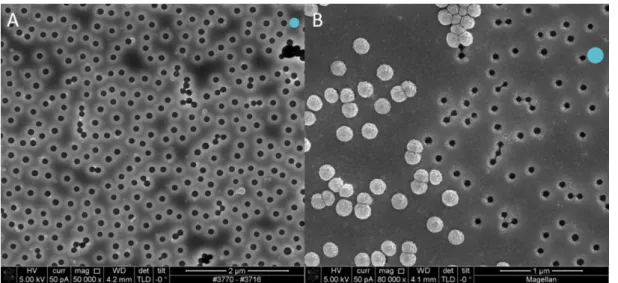
The final structure depicted in Figure 4.4 is obtained after removing the polymer and the metal with acetone. It is represented in this figure samples with the top disk deposited at A) 0 ° and B) 6 °. It is possible to observe some defects that can happen during the structures’ fabrication (besides the already discussed disk aggregation). In Figure 4.4A, there are a couple of structures that are slightly bigger than the others. Such result is unavoidable since the colloidal solution has some particles that may be bigger. On the other hand, in Figure 4.4B, there are some particles that are not complete or have something extra in the structure. This is caused by defects on the mask, where the holes may not have closed evenly and thus, the top disk was deposited in the wrong place while there is one which does not have any disk at all on top. Again, it is caused by the particles’ size dispersion and, as the holes were being shrunk, this hole may have been completely closed, not allowing for a second gold deposition. However, whichever the case, and not accounting the aggregation observed in Figure 4.4A, since they are only two or three cases in the whole image, they will not affect considerably the extinction measurements.
15
Through Figure 4.2 to Figure 4.4, it is possible to see that the pattern is maintained throughout the whole process as well as the top-bottom disks centre’s distance. In fact, using ImageJ and a MATLAB script for several SEM pictures of the 6 ° deposition, the lower disk diameter is estimated on (118 ± 6) nm (of 730 particles analysed, taken from 3 pictures) and the upper disk diameter is estimated on (55 ± 6) nm (of 737 analysed particles from the same 3 pictures as the previous ones). It is important to note that all particles were assumed to be circular for these calculations. The deviation on the big disk size is in agreement with the relative deviation of the original particle size. As shown in Figure 4.4, there are some big particles without a small one on top. However, the fact that the script calculated more small particles than big ones has to do with the fact some small particles were broken and when processing the images, a small particle could be considered as two to correctly analyse the whole picture. Even with this limitation, the absolute standard deviation of both kind of disks are approximately the same, proving this a good method to consistently shrink the holes on the mask. It was also possible to
determine the disks’ centres of mass distance between the top and bottom using the same script in
MATLAB, which is estimated at (27 ± 4) nm. Being this distance roughly half the small disk radius, it is thus shown mathematically that the top disk is close to the edge.
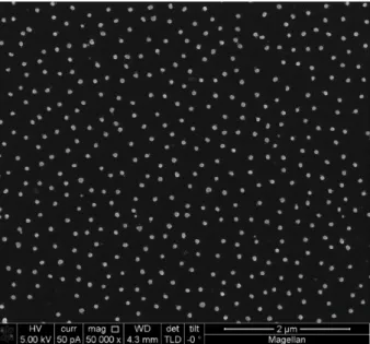
Then, to see how the individual disks would respond, samples with only the big disks and then only the small disks were fabricated. To ensure that the small disk would have the same size as if it were fabricated with the big gold disk, SiO2 was deposited to replace the big gold disk. As mentioned before,
Au has a sidewall angle of 11.7 ° while SiO2 has an angle of 47.2 °. This means that, to replace a 20 nm
thick disk with SiO2, it should be deposited 3.9 nm of the insulator material as suggested by Figure 4.5.
The deposition rate used for this material was 0.3 Å/s.
Figure 4.5 - Schematic of the small disk fabrication. The materials used are the same except the bottom disk, which is 3.9 nm high SiO2 (depicted in black) instead of Au.
Development of Plasmonic Nanosandwiches for Biosensing Applications
16
On the samples with small disks fabricated this way, it was observed a total of 2002 small disks with a diameter of (69 ± 8) nm. Although these disks are slightly bigger than the ones fabricated on top of the big gold disks, they are enough for the purpose intended. This increase may have to do with the SiO2 itself, since it is a very difficult material to deposit using an e-beam evaporation technique (the
observed deposition rate was not perfectly 0.3 Å/s) together with a low thickness which may have resulted in a different real thickness than desired. In this picture, it is more evident the non-circular shape of the small particles, a limitation of the mask-shrinking process.
Finally, the desired sensing structure was designed to have only the top disk exposed. Using a different etching machine, holes were etched on the quartz substrate, so it would be possible to deposit the big disk inside said hole. The following Al deposition would cover the disk’s surface. Figure 4.7A shows a SEM picture of the holes (and part of the hole mask that remained on the sample) while Figure 4.7B shows the holes with the first layer of gold deposited.
Figure 4.7 – SEM pictures of A) etched holes on quartz and B) etched holes filled with gold of 20 nm height, also on quartz. Both pictures were taken with the sample tilted at 50 °.
17
Finally, in Figure 4.8, it is possible to see two full structures with the bottom disk inside the hole. Using this method, it is possible to do such a thing. There is a circular residue around the structure that is related to the polymer. It was very uncommon to appear on the samples’ surface, but it can be properly removed with a plasma cleaning.
Figure 4.8 – Two nanosandwhich strucutres inside a hole made on the quartz substrate. The samples were tilted at 57 °.
4.2.
Extinction Measurements
–
Experimental and Simulations
The following spectra may show a discontinuity at 900 nm. It was generated by the equipment when changing the grating system to access different spectral range and should be ignored.
In Figure 4.9, it is shown the spectra for the individual disks, both the big disks (in black) on their own and the small disks (in red) made on top of a SiO2 base.
Development of Plasmonic Nanosandwiches for Biosensing Applications
18
The difference in the peak position is purely due to the size of the disk and the number of electrons available to oscillate. The relevant aspect to discuss, however, is the signal given by both disks. The smaller disk has a much lower signal than the big disk. In this case, it is not the different number of disks in each case that causes this, as the big disk samples had an average particle density of (8.2 ± 0.2) particles/µm2 while the small disks samples have an average density of (13.0 ± 2.2) particles/µm2. The
lower signal can prove difficult to monitor the wavelength peak change due to a lower signal to noise ratio. This is the reason to try a structure which can use the high signal that comes from the bigger interaction with the incident light from the big disk and the high sensibility from the smaller disk.
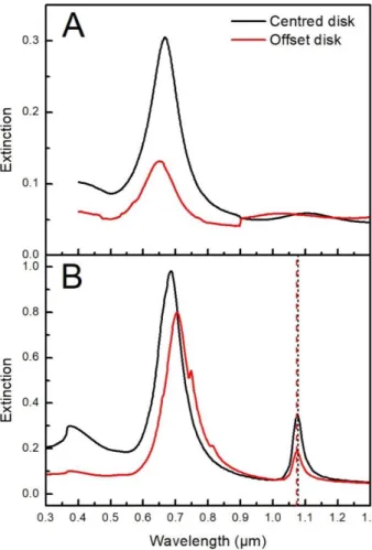
For that, a full structure on glass was fabricated and had its light extinction measured, with the top disk in the centre of the structure and by the edge of the bottom disk, with results shown in Figure 4.10, both experimental and simulated.
Figure 4.10 – A) Experimental extinction spectra for full structures and B) simulated transmission spectra for the the same structures. In both, the black line corresponds to the top disk centrered with respect to the bottom one and the red corresponds to the offset disk, placed at the edge.
19
Starting the peak analysis from the low energy (LE) peaks (i.e. longer wavelengths, at around 1075 nm), the simulation suggests that there is no difference on the optical response of the structures when moving the top disk around the structure apart from a minimal shift (indicated by the dashed lines), which will be further discussed when looking at the field plots. This peak is caused by a purely plasmonic gap mode on the insulator layer and the energy confinement inside the gap. Only the shift’s direction occurs in the experimental set, not the magnitude of it. It is suggested that the FDTD model cannot replicate the magnitude of the blue-shift because it only simulates on a single, well defined structure, which does not happen experimentally. The disks are subjected to process variability on their geometry, more prominently the top disk, heavily influencing the peak position. Also, the mismatch on the peak positions may be due to the overestimation of the oxide’s refractive index on the simulation, as the software does not take into account quantum effects that may occur when dealing with structures this thin8.
Moving on to the high energy (HE) peak, the results are seemingly contradictory. While the experimental set shows a blue-shift, the simulation reveals a red-shift when the disk is moved around. The red-shift on Figure 4.10B is that the Z component of the electric field (Figure 4.13A) is not symmetric along the surface that corresponds to the gap, which would suggest that the electrons would be more
spread over in such a way, so it could lower the system’s overall energy. Also, this HE peak shows
some peak/dip features on the offset structure in the simulated spectrum. These are due to the excitation of higher order multipoles through the energy given by the overall structure, resulting in a Fano resonance8,15. The fact that they only show up in the offset structure implies that it is easier to excite
these multipoles when the disk is not centred. Its absence on the experimental set experimental set may be caused by the experimental polydispersity, which would broaden and smoothen the sharp peak (since it would happen at different wavelengths for different structures). Once again, the simulation deals with only one structure while the actual experimental structures have some degree of variability (different radii between disks, for instance). Due to this absence, no further study was made on such peaks.
The blue-shift on Figure 4.10A may be caused by imperfect structures. Recalling the distance calculations, (27 ± 4) nm between the centres the big and small disks, some disks have fallen over the bottom ones, making one complex structure instead of two separate disks.
In the simulation, it is also shown a peak at around 375 nm, which corresponds to the interband transitions of gold40. The experimental spectra also show an increasing extinction towards these
wavelengths, but the measurements were only performed until 400 nm.
Next, in Figure 4.11, it is represented the spectra for the structure with the top disk in the centre, only varying the alumina layer thickness from 3 nm to 6 nm.
Development of Plasmonic Nanosandwiches for Biosensing Applications
20
structure would be reduced. As the separation increases, the disks are not as strongly coupled as they were, resulting in a weaker cancelation and a higher dipole energy8.
Figure 4.11 - A) Experimental extinction spectra for full structures and B) simulated transmission spectra for the the same structures. In both, the black line corresponds to a disk separation by Al2O3 of 3 nm and the red line to a disk
separation of 6 nm.
As for the HE peak, there is again a disagreement between the shift’s direction. However, it should be taken in consideration that it is highly likely that the upper disk on the 6 nm thick oxide structure may be smaller than in the 3 nm thick disk as an extra deposition occurred (and further oxidation, which shrunk the hole even more); the simulated structure may have not been properly designed, giving a different overall geometry.
4.3.
FDTD Field Plots
Figure 4.12 and Figure 4.13 show electric field distribution plots for the studied structures. The xy
-plane contains the bottom face of the bottom gold disk and the disks are stacked along the z-axis,
coinciding with the propagation of the incident light. In Annexe C – Additional Electric Field Plots it is possible to see the same plots in logarithmic scale instead.
Figure 4.12 shows the z-component of the electric field obtained for all simulated scenarios for the
21
explained by the fact that the red component is slightly shorter than the blue one. This inequality may imply a different charge distribution on the disks, which could lead to an increase on the gap’s energy. The disks’ electrons can only oscillate between the metal boundary, they cannot leave the material. As such, the top disk’s one cannot oscillate further away from the centre of the bottom disk, since that is where the top disk ends, whereas the bottom disk’s electrons can oscillate beyond this point, leading to a more spread over electron distribution towards the opposite side of the top disk. This fact may cause the uneven gap electric field distribution.
Figure 4.12 –z-component electric field plots obtained for the respective low energy peak wavelength of the A) and
B) offset structure with 3 nm spacer, C) and D) centered structure with 3 nm spacer and A) and B) centred structure with 6 nm spacer. A), C) and E) are obtained from the bottom disk/alumina interface while B), D) and F) is a cross-section that goes through the centre of the top disk. The dashed lines represent the perimeter of the different components of the structure.
Development of Plasmonic Nanosandwiches for Biosensing Applications
22
It should be considered that the scale on Figure 4.12F goes to around ±125 because of the small region on the spacer/top disk interface. This happens because the software breaks down the structures in small cubes, and this structure in particular has a sidewall, which will make sharp edges, known to be enhancement hotspots. Therefore, although this structure’s gap has a superior field enhancement (the absolute value goes up to around 70), even higher enhancements for individual pixels are achieved but are not physically meaningful.
Next, Figure 4.13 is the same as Figure 4.12, this time at the HE peak wavelength.
Figure 4.13 –Z-component electric field plots obtained for the respective high energy peak wavelength of the A)
23
Again, and contrary to expected, there is also a high field enhancement on the spacer layer. However, there is also enhancement on the vicinity of the structures (more prominent near the edges), leading to a net dipole moment for the overall structure. So, it can be concluded that the HE peak is given by the interaction between the gap mode and antibonding mode.
The electric field enhancement near the disks (and outside the gap) have approximately the same enhancement factor on the z direction (around 5), indicating that both position on the top disk and spacer
thickness don’t have much influence on the field’s enhancement. The gap however seems to be influenced by both parameters, and it is more intense on the centre disk structure separated by 3 nm thick spacer (Figure 4.13D), whereas on the other two configurations, the influence is of the same importance, even though the field shape is not symmetric. This asymmetry may have to do with the charge distribution inside the metallic materials.
25
5.
Conclusions and Future Perspectives
This work intended to develop a fabrication procedure to a stacked disk pair of different diameters for biosensing applications. So far, to use only the top disk as the sensing structure, the fabrication process has shown promising results, since it seems to be possible to bury the bottom disk in a quartz hole underneath an alumina layer. The structure that should be further studied to learn about its biosensing capabilities should be the thin insulator layer (3 nm) with the top disk on the centre. This has shown to have a higher electric field enhancement around the structure compared to the others studied.
To make sure that the bottom disk is in fact isolated, one could deposit the bottom disk and the aluminum layer and oxidise it and immerse the sample in an alkanethiol solution since they should bind to gold. The sample would then be inspected through XPS and it is desired the absence of these alkanethiols.
A next approach to study the structure’s potential use as a biosensor would be to use alkanethiols again, but with different carbon lengths and make extinction spectra. The idea would be to see how much the peak would shift with different refractive index in a thin film case rather than bulk surrounding media. In principle, the HE peak should be the one to be monitored. Not only because it is the one with higher intensity, but the LE peak is mainly related to the gap mode, where the biosensing will not happen.
Another important aspect is the optimisation of the entire process. As seen in the fabrication process, some issues have come up, specially the substrate etching process. First it is important to know the nature of the debris observed in Figure 4.7B, possibly through XPS. If in fact those debris are residual amorphous SiO2 from the substrate, the polymer should be thinner to maximise the amount of SiO2 that
leaves through the hole or use other polymer etching parameters so that the sidewall etching can be higher and for that reason, some of the silica that sticks to the wall is further from the disk and lower the probability that falls over the structure.
27
6.
References
1. Baptista, P., Doria, G., Henriques, D., Pereira, E. & Franco, R. Colorimetric detection of eukaryotic gene expression with DNA-derivatized gold nanoparticles. J. Biotechnol.119, 111–117 (2005).
2. Larsson, E. M., Alegret, J., Kǎll, M. & Sutherland, D. S. Sensing characteristics of NIR localized surface plasmon resonances in gold nanorings for application as ultrasensitive biosensors. Nano Lett.7, 1256–
1263 (2007).
3. Rechberger, W. et al. Optical properties of two interacting gold nanoparticles. Opt. Commun.220, 137–
141 (2003).
4. Jain, P. K., Huang, W. & El-Sayed, M. A. On the universal scaling behavior of the distance decay of plasmon coupling in metal nanoparticle pairs: A plasmon ruler equation. Nano Lett.7, 2080–2088 (2007). 5. Wersäll, M. et al. Directional nanoplasmonic antennas for self-referenced refractometric molecular
analysis. J. Phys. Chem. C118, 21075–21080 (2014).
6. Prodan, E., Radloff, C., Halas, N. J. & Nordlander, P. A Hybridization Model for the Plasmon Response of Complex Nanostructures. Science (80-. ).302, 419–422 (2003).
7. Frederiksen, M., Bochenkov, V. E., Cortie, M. B. & Sutherland, D. S. Plasmon hybridization and field confinement in multilayer metal-dielectric nanocups. J. Phys. Chem. C117, 15782–15789 (2013). 8. Frederiksen, M., Bochenkov, V. E., Ogaki, R. & Sutherland, D. S. Onset of bonding plasmon hybridization
preceded by gap modes in dielectric splitting of metal disks. Nano Lett.13, 6033–6039 (2013). 9. Song, J. & Zhou, W. Multiresonant Composite Optical Nanoantennas by Out-of-plane Plasmonic
Engineering. Nano Lett.18, 4409–4416 (2018).
10. Dmitriev, A., Pakizeh, T., Käll, M. & Sutherland, D. S. Gold-sitica-gold nanosandwiches: Tunable bimodal plasmonic resonators. Small3, 294–299 (2007).
11. Maier, S. A. Plasmonics: Fundamentals and Applications. (Springer US, 2007).
doi:10.1016/j.aca.2010.06.020
12. Wei, W., Zhang, X., Yu, H., Huang, Y. & Ren, X. Plasmonic waveguiding properties of the gap plasmon mode with a dielectric substrate. Photonics Nanostructures - Fundam. Appl.11, 279–287 (2013). 13. Atwater, H. A. & Polman, A. Plasmonics for improved photovoltaic devices. Nat. Mater.9, 205–213
(2010).
14. Mendes, M. J., Morawiec, S., Simone, F., Priolo, F. & Crupi, I. Colloidal plasmonic back reflectors for light trapping in solar cells. Nanoscale6, 4796–4805 (2014).
15. Luk’Yanchuk, B. et al. The Fano resonance in plasmonic nanostructures and metamaterials. Nat. Mater. 9, 707–715 (2010).
16. Jørgensen, A. M. Design and Fabrication of Plasmonic Metasurfaces Based on Metallic Dimer Arrays. (Aarhus University, 2017).
17. Ferhan, A. R., Jackman, J. A., Park, J. H., Cho, N. J. & Kim, D. H. Nanoplasmonic sensors for detecting circulating cancer biomarkers. Adv. Drug Deliv. Rev.125, 48–77 (2018).
18. Zhou, W., Gao, X., Liu, D. & Chen, X. Gold Nanoparticles for in Vitro Diagnostics. Chem. Rev.115,
10575–10636 (2015).
19. Ciui, B., Jambrec, D., Sandulescu, R. & Cristea, C. Bioelectrochemistry for miRNA detection. Curr. Opin. Electrochem.5, 183–192 (2017).
20. Yu, Q. et al. Luminescent gold nanocluster-based sensing platform for accurate H 2 S detection in vitro
and in vivo with improved anti-interference. 1–11 (2017). doi:10.1038/lsa.2017.107
21. Zhu, S., Li, H., Yang, M. & Pang, S. W. High sensitivity plasmonic biosensor based on nanoimprinted quasi 3D nanosquares for cell detection. Nanotechnology27, 295101 (2016).
22. Chang, C., Lin, H., Lai, M., Shieh, T. & Peng, C. Flexible Localized Surface Plasmon Resonance Sensor with Metal – Insulator – Metal Nanodisks on PDMS Substrate. Sci. Rep. 1–8 (2018).
doi:10.1038/s41598-018-30180-8
23. Fredriksson, H. et al. Hole-mask colloidal lithography. Adv. Mater.19, 4297–4302 (2007).
24. Li, G., Shen, Y., Xiao, G. & Jin, C. Double-layered metal grating for high-performance refractive index sensing. Opt. Express23, 8995 (2015).
25. Jain, P. K. & El-Sayed, M. A. Plasmonic coupling in noble metal nanostructures. Chem. Phys. Lett.487,
153–164 (2010).
26. Li, M., Cushing, S. K. & Wu, N. Plasmon-enhanced optical sensors: A review. Analyst140, 386–406
(2015).
27. Boriskina, S. V. & Reinhard, B. M. Molding the flow of light on the nanoscale: From vortex nanogears to phase-operated plasmonic machinery. Nanoscale4, 76–90 (2012).
28. Cordeiro, M., Ferreira Carlos, F., Pedrosa, P., Lopez, A. & Baptista, P. Gold Nanoparticles for Diagnostics: Advances towards Points of Care. Diagnostics6, 43 (2016).
29. Anker, J. N. et al. Biosensing with plasmonic nanosensors. Nat. Mater.7, 442–453 (2008).
30. Kuttge, M., García De Abajo, F. J. & Polman, A. Ultrasmall mode volume plasmonic nanodisk resonators.
Nano Lett.10, 1537–1541 (2010).
31. Nordlander, P., Oubre, C., Prodan, E., Li, K. & Stockman, M. I. Plasmon hybridization in nanoparticle dimers. Nano Lett.4, 899–903 (2004).
Development of Plasmonic Nanosandwiches for Biosensing Applications
28
33. Cui, Z. Nanofabrication: Principles, Capabilities and Limits. (Springer US, 2008).
doi:10.1007/978-0-387-75577-9
34. Chen, Y. Nanofabrication by electron beam lithography and its applications: A review. Microelectron. Eng. 135, 57–72 (2015).
35. Zhang, G. & Wang, D. Colloidal lithography - The art of nanochemical patterning. Chem. - An Asian J.4,
236–245 (2009).
36. Kontio, J. M., Simonen, J., Tommila, J. & Pessa, M. Arrays of metallic nanocones fabricated by UV-nanoimprint lithography. Microelectron. Eng.87, 1711–1715 (2010).
37. Frederiksen, M. & Sutherland, D. S. Direct modification of colloidal hole-masks for locally ordered hetero-assemblies of nanostructures over large areas. Nanoscale6, 731–5 (2013).
38. Lide, D. R. CRC Handbook of Chemistry and Physics. (CRC Press, 2003).
39. Palik, E. D. Handbook of Optical Constants of Solids. (Academic Press, 1991).