Abstract
—
This article describes the design of a dual-wideband
annular slot antenna. The proposed structure has been optimized to
operate in the typical bands of mobile communication systems
(0.824-0.960 GHz and 1.710-2.165 GHz). The antenna is designed
considering two independent ports with high isolation, one for each
operation band, yielding an antenna that exhibits diplexing feature.
The final measured results show that the designed antenna exhibits
stable radiation pattern over the frequency in both desired bands.
The designed antenna has been used to compose a dual-band linear
array. Simulation results indicate good performance in both bands
for mobile communication systems.
Index Terms— dual-band antenna arrays, multi-band antennas, printed antennas, slot antennas.
I.
INTRODUCTIONDual-band antennas find applications in several areas, such as in mobile communications and satellite navigation systems. The antenna configuration to achieve multiband behavior can be in stacked or coplanar form [1]. Stacked patches have been used in several antenna designs [2]—[5] and have the advantage of allowing broadband or dual-band behavior. The drawback is the need of a multilayer structure for the assembly, which makes the design and fabrication more complex, hence increasing the fabrication costs. Dual-band operation can be achieved as well with coplanar microstrip structures, whereby a canonical patch geometry is generally modified by the inclusion of slots [6]—[12] or by employing fractal-based geometries [13], [14].
Mobile communication is an example of a system based on multi-band operation. A significant number of printed antennas for radio-base stations have been developed and are reported in the literature. The antenna proposed in [15] is a compact dual-feed dual-polarized patch antenna with bands centered at 0.9 GHz and 1.8 GHz. The antenna has a stacked arrangement and its integration into an array is difficult due to the complex feeding system necessary for dual-band operation. Similarly, the antennas presented in [16]—[18] have also a stacked arrangement. They exhibit good performance, but are not well-suited for low-cost solutions.
Alternatively to antennas implemented in microstrip configuration, printed slot antennas have been studied and can be assumed as a solution with lower cost compared to the stacked configuration. In [19], a dual-band annular slot antenna has been studied. It exhibits bidirectional pattern and narrow-band behavior, hence it is not
Dual-Port Dual-Wideband Annular Slot
Antenna with Stable Unidirectional Pattern
R. L. Farias,
Instituto de Telecomunicações, Instituto Superior Técnico -- Universidade de Lisboa (IST-UL), 1049-001 Lisboa, Portugal
D. L. Lemes, J. M. Vieira, M. V. T. Heckler
Laboratory of Electromagnetics, Microwaves and Antennas (LEMA), Universidade Federal do Pampa (UNIPAMPA), 97546-550 Alegrete, RS, Brazil, Phone: +55 55 3421 8400, E-mail:
A. F. T. Salazar
suitable to be employed for sector radio-base stations. In [20], a dual-band annular slot antenna was designed for wide-band applications, but it also exhibits bidirectional radiation patterns. In [21], [22], unidirectional radiation pattern has been achieved considering a metallic cavity added at the back of the annular slots. A cavity-backed annular slot antenna proposed in [23] provides dual-band feature with two concentric slot-rings and stable radiation pattern in both bands, but the dimensions of the cavity were too large, hence resulting in a bulky structure unsuitable for array design.
In this paper, a compact dual-feed dual-band slot antenna is described. It has been designed to operate in the frequency bands of 0.824 – 0.960 GHz (15% bandwidth) and 1.710 – 2.165 GHz (23% bandwidth), which are typical for mobile communication systems. In comparison to the antenna reported in [23], area reduction of 46% has been achieved whilst keeping nearly the same performance. This allows employing the designed antenna to compose a linear array with dual-band operation, in contrast to the two array configuration normally used in commercially available radio base sector antennas. The other challenges achieved with the proposed antenna are the operation in two wide bands with two highly isolated ports, whilst keeping its fabrication simple. Moreover, the unidirectional radiation pattern obtained remains stable in shape and with the same polarization over the frequency. In the next section, the geometry of the proposed antenna is described, whereby the physics and the main design parameters are discussed. In Section III, the prototype is shown and the numerical results obtained with Ansys HFSS are compared to measured data. Parametric simulations are shown in order to explain the discrepancies verified between numerical and measured results. Experimental tunning has been carried out to compensate for the fabrication errors. Section IV is dedicated to the assessment of the proposed antenna to compose a dual-band linear array, which is suitable to operate as a sector base-station antenna.
II.
C
OMPACTD
UAL-F
EEDD
UAL-B
ANDA
NNULARS
LOT ANTENNAThe main design parameters of annular slot antennas are the slot radius 𝑅𝑠, the slot width 𝑊𝑠 and the length of the open-ended stub. The antenna resonance frequency is governed mainly by 𝑅𝑠, which can be calculated by
𝑅𝑆=2𝜋𝜆𝑔
(1)
where 𝜆𝑔 is the guided wavelength in an equivalent slotline with width 𝑊𝑠. As an initial estimate, the guided wavelength can be obtained approximately by numerical techniques applied to the slotline. The slot width 𝑊𝑠 can be used to control the antenna bandwidth. Additionally, it plays a secondary role on the antenna resonance frequency and can be used eventually for fine tune, as demonstrated in [24].
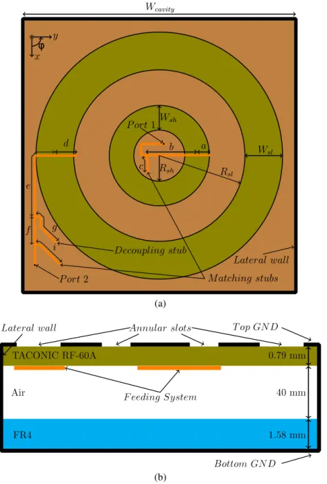
For dual-band applications, two concentric slots can be used with the schematic top view as illustrated in Fig. 1a. The main design parameters are the radii (𝑅𝑠𝑙 and 𝑅𝑠ℎ for the larger and the smaller slots, respectively), and the slot widths (𝑊𝑠𝑙 and 𝑊𝑠ℎ for the larger and the smaller slots, respectively). Both dimensions 𝑅𝑠𝑙 and 𝑅𝑠ℎ can be found employing (1) by considering 𝜆𝑔 in the center frequency of each band.
both top and bottom GNDs. Hence the cavity helps to focus the radiated power to the boresight and increases the overall antenna gain.
(a)
(b)
Fig. 1. Compact dual-feed dual-band annular slot antenna: (a) Top view; (b) Cross-sectional view.
The cavity dimensions have large influence on the antenna input impedance. A study on this topic has been presented in [26]. By varying the thickness of the air layer, the operation band is shifted. The bandwidth becomes narrower by approximating the bottom GND to the annular slots. Hence this parameter, along with 𝑊𝑠𝑙 and 𝑊𝑠ℎ are very important to obtain the desired antenna operation. The lateral dimensions 𝑊𝑐𝑎𝑣𝑖𝑡𝑦 are chosen to be as small as possible, so as to allow this antenna to be used to compose an array [27].
open-ended, quarter-wave long stub tuned at 1.9 GHz, so as to produce nearly total reflection of waves in the higher operation band. After introducing the decoupling stub, impedance matching is also achieved with the single stub technique for the lower band. No decoupling stub was necessary in the feed line for the higher band; hence the matching for the inner annular slot was achieved with the conventional single-stub technique.
The design and optimization of all dimensions of the antenna have been carried out using Ansys HFSS [28]. The optimized geometric parameters are as follows: a = 7.25 mm, b = 28.0 mm, c = 9.0 mm, d = 12.4 mm, e = 43.7 mm, f = 15.5mm, g = 19.0 mm, i = 23.0 mm, Wsh = 13.5 mm, Rsh = 14.0 mm, Wsl = 20.7 mm, Rsl = 47.0
mm. The air layer has been included to increase the separation of the GND to the slots. After some simulations, the air layer thickness was set to 40 mm, which is the trade-off between antenna volume and bandwidth. In addition, the lateral dimensions of the cavity are Wcavity = 150 mm yielding an area reduction of 46% relative to the antenna described in [23].
III.
P
ROTOTYPE ANDM
EASUREDR
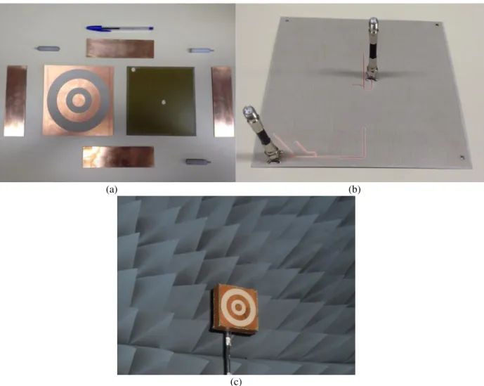
ESULTSA prototype of the designed antenna has been built and photos prior to and after the final assembly are shown in Fig. 2. In order to receive/transmit the signals properly, surface-mount connectors have been employed. Since the connectors are inside the cavity, coaxial cables are used as an extension to the rear part of the antenna. These cables have been included in the electromagnetic model, since they modify the electromagnetic field configuration in comparison to an ordinary homogeneous cavity.
(a) (b)
(c)
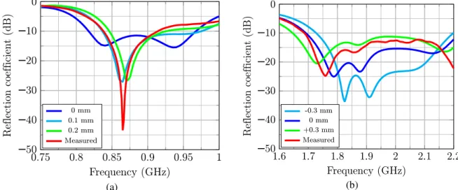
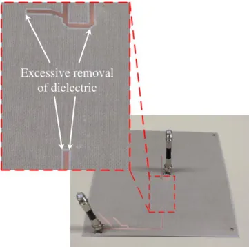
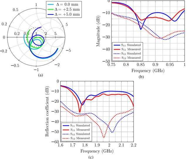
The reflection coefficient at each port has been measured and the results are shown in Fig. 3a and b, where the blue curve stands for the simulation results and the red curve represents the measurements. For the lower band, large discrepancy between numerical and experimental results is verified. The bandwidth obtained in the measured data is narrower than the simulated curve, showing a reduction of 51% compared to the desired bandwidth. Better performance is observed for the higher band, whereby the experimental curve complies with the band specified previously. In order to find the reason for the discrepancies between numerical and experimental results in the lower band, parametric simulations have been performed by varying the dielectric constant of the laminates and the air layer thickness. The simulations showed that these two parameters have only little influence on the reflection coefficient in the lower band. By inspecting the feeding system, one can see that the milling machine used to etch the laminates removed part of the dielectric layer in the contour of the lines. This is shown in detail in Fig. 4.
The excessive etching of dielectric has been included in the HFSS model. Simulated results are presented in Fig. 3a (green and cyan curves), where one can see the variation of the reflection coefficient for the lower band as a function of the milling depth into the dielectric around the feed lines. The simulations show that even small milling depths have great impact on the antenna input impedance. The agreement between simulations and measurements improves strongly with the addition of milling imperfection. The changes can be explained by considering that the removal of the dielectric along the edges of the feed lines is equivalent to replace the dielectric material (𝜀𝑟 = 6.15) by air (𝜀𝑟 = 1.00). This makes the effective dielectric constant to be reduced due to the modification on the electromagnetic field distribution that propagates in the lines of the 𝜀𝑟 feeding system. Hence the guided wavelength and the characteristic impedance of the lines are changed.
(a) (b)
Fig. 3. Reflection coefficient calculated during the parametric analyses of the constructed prototype: (a) Variation in the lower band as a function of milling depth of dielectric; (b) Variation in the higher band as a function of misalignment
Fig. 4. Excessive removal of dielectric during fabrication of the feeding system.
Misalignment between the annular slots and the feeding system during the fabrication has been studied too. The reflection coefficient changes strongly in the higher band for misalignment along the y-direction as shown in Fig. 3b. For misalignment along the positive y-direction, a little shift towards lower frequencies is verified and the agreement between simulations and measurement improves.
The parametric simulations presented in Fig. 3 show that the modelling of dielectric etching provided better agreement between the simulated and measured curves in the lower band, whereas the misalignment between the annular slots and the feeding system resulted in larger changes in the higher band curves. In order to model correctly the imperfections of the constructive process, both the dielectric milling and misalignment have been added simultaneously in the HFSS model. After parametric simulations, the best agreement between the new model and the measurements has been obtained by considering dielectric milling with 0.25 mm depth and 0.4 mm width, and misalignment along the positive y-direction of 0.35 mm.
In order to correct the antenna response in the lower band without the fabrication of a new prototype, an experimental optimization strategy for the feeding system of the lower band has been considered. By analyzing the Smith chart illustrated in Fig. 5a, one can see that it is possible to move the loop of the experimental curve into the VSWR = 2.0 circle only by adjusting the length of the matching stub of the feeding system for the larger slot. Parametric simulations for the stub length variation Δ have been carried out and the results are shown in Fig. 5a. The best result was obtained when the matching stub length is increased by 5 mm from the previously optimized length.
(a) (b)
(c)
Fig. 5. Experimental optimization of the prototype: (a) Variation of the input impedance with the matching stub length; (b) Final simulated and measured results for the lower band; (c) Final simulated and measured results for the higher band.
The simulated and measured results for both bands with the larger matching stub are shown in Fig. 5b and Fig. 5c. In the lower band, one can observe that the length compensation strategy of the stub was successful, since the whole desired band is now matched. In the higher band, good agreement between theoretical and measured results also exists. The prototype presents now a bandwidth allocated at frequencies 1.687 – 2.2 GHz (27%), whereby the requirement of the bandwidth was adequately satisfied for the higher band too. Furthermore, the isolation between ports 1 and 2 in both bands is larger than 17 dB, hence confirming the high isolation between the two outputs.
(a) (b)
(c) (d)
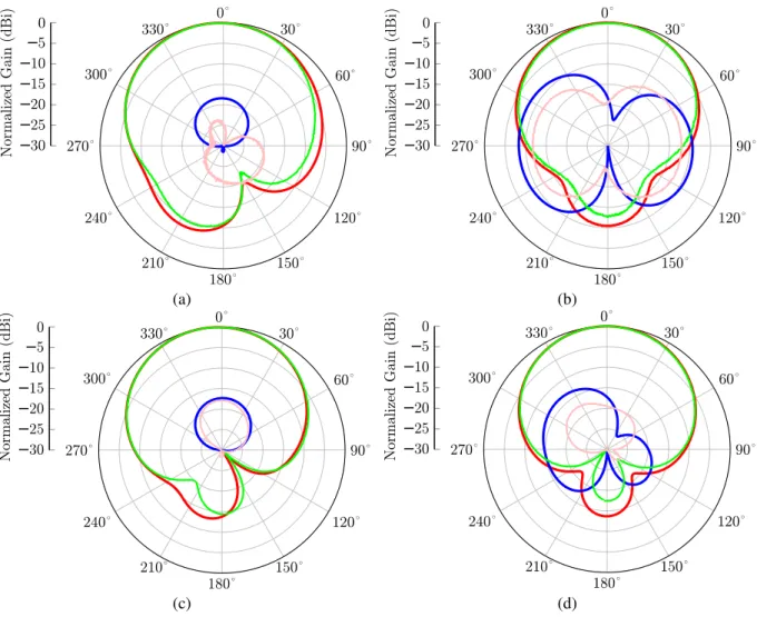
Fig. 6. Measured and simulated radiation patterns in the lower band. The curves are coloured as follows: Simulated co-polarization (red), simulated cross-co-polarization (blue), measured co-co-polarization (green) and measured cross-co-polarization
(a) (b)
(c) (d)
Fig. 7. Measured and simulated radiation patterns in the higher band. The curves are coloured as follows: Simulated co-polarization (red), simulated cross-co-polarization (blue), measured co-co-polarization (green) and measured cross-co-polarization
(pink).
(a) (b)
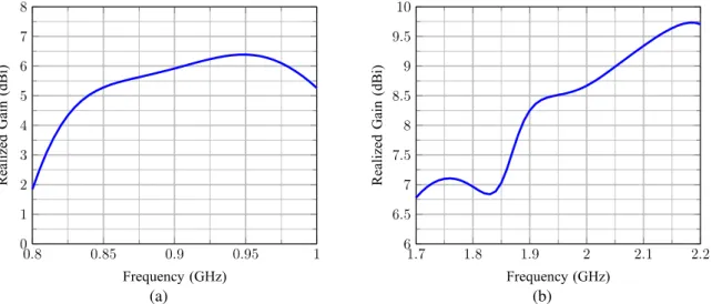
Fig. 8. Realized Gain of the proposed antenna throughout the two resonant bands: (a) lower band; (b) upper band.
IV.
D
UAL-B
ANDN
ON-U
NIFORMLYS
PACEDL
INEARA
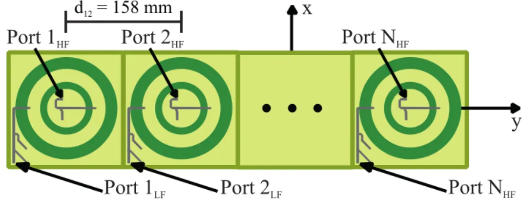
RRAYDue to the high isolation obtained between the ports related to each operation band, the antenna
since it allows performing beamforming for each band independently. The basic array geometry is
shown in Fig. 9, where d
ijstands for the distance between the
i
-th and the
j
-th elements. Due to the
size of the cavity of each element, the minimum possible center-to-center inter-element spacing is 158
mm, so that the antennas do not overlap. This spacing corresponds to roughly 0.5
𝜆
0and
𝜆
0at the
center frequencies of the lower (900 MHz) and higher (1900 MHz) bands, respectively.
Fig. 9. Dual-band antenna array with uniformly spaced elements for mobile communications.
Due to the different electrical inter-element spacings at each band, combined with periodicity
present in the uniform linear array (ULA) geometry, grating lobes will appear in the pattern of the
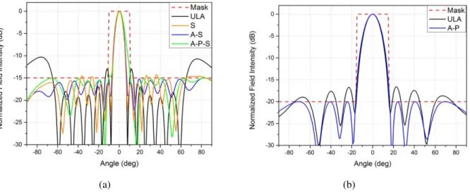
higher band, as it can be verified in Fig. 10a. The black curve corresponds to the pattern obtained by
feeding all the elements with the same excitation coefficient.
To assess the performance of the designed antenna to operate as an array, two scenarios have been
considered: main beam pointing to the boresight with suppression of grating and side lobes, and
beamshaping the main beam to follow a squared-cosecant contour. The analyses have been carried out
considering an array with 7 dual-band antennas. Particle swarm optimization (PSO) has been used to
determine the optimum excitation coefficients for each case. This technique has been already
employed successfully for interelement spacings smaller than
𝜆
0[29]. The optimizations are done
(a) (b)
Fig. 10. Optimized patterns with the main beam pointing to 0$^\circ$: (a) higher band; (b) lower band.
The first scenario considered is an array with the main beam pointing to the boresight and with side
lobe level (SLL) control. The uniform spacing (158 mm) between the elements is equal to
𝜆
0at 1.9
GHz. As mentioned above, such a large distance between the antennas yields grating lobes in the
pattern of ULAs. Grating lobes are a consequence of the vector sum of the radiated fields in directions
other than the desired main beam and can be only mitigated if the periodicity present in ULAs is
broken. This can be achieved with non-uniformly spaced arrays, whereby the inter-element spacings
are not the same and can be properly optimized to improve the radiation performance. In Fig. 10a, the
results for three optimization cases are shown. In the desired mask, the grating lobe levels should be
kept 15 dB below the main beam. The orange curve stands for the optimization of the inter-element
spacings only (S) whilst keeping the amplitudes and phases of the feeding currents the same for all the
elements. The blue curve stands for the results when the amplitudes of the excitation coefficients and
the inter-element spacings (A-S) are optimized simultaneously. Finally, when the phases of the
excitation coefficients are also included in the optimization (A-P-S), the green curve is obtained. The
results indicate that the grating lobes could be well suppressed. The last two approaches (S and
A-P-S) resulted in patterns that fulfill the specified mask.
In the lower band, the elements are electrically closer to each other, hence no grating lobes exist
and the levels of the side lobes are also lower. At 900 MHz, the optimization mask is set so as to keep
the side lobe level (SLL) 20 dB below the main beam. By taking the non-uniform positions optimized
for the higher band and performing optimization of only the amplitudes and phases of the excitation
coefficients, the optimized pattern for the lower band is shown in Fig. 10b. One can see that the
patterns for both bands point to the boresight with full control of the side lobe and grating lobe levels.
TABLE I.INTER-ELEMENT SPACINGS FOR THE OPTIMIZED DUAL-BAND ANTENNA ARRAY
Inter-element spacing (mm)
d12 158
d23 158
d34 158
d45 158
d56 158
d67 257.7
TABLE II.EXCITATION COEFFICIENTS FOR RADIATION IN THE BORESIGHT WITH SUPPRESSION OF GRATING AND SIDE LOBES
Port Normalized amplitude Phase Port Normalized amplitude Phase
1LF 0.254 186.066º 1HF 0.245 170.011º
2LF 0.306 221.763º 2HF 0.559 183.928º
3LF 0.362 243.678º 3HF 0.943 177.706º
4LF 0.527 223.296º 4HF 0.962 166.732º
5LF 0.356 236.000º 5HF 1.000 146.026º
6LF 0.951 238.085º 6HF 0.196 91.838º
7LF 1.000 219.669º 7HF 0.578 165.931º
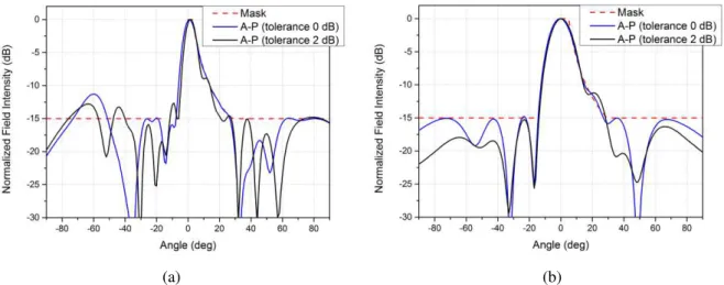
The second scenario is the synthesis of the dual-band array with the main beam exhibiting squared
cosecant shape and SLL control. The shaped beam should perfectly follow the squared-cosecant
contour (angular region between 0º and 30º), whereas it should be below -15 dB for other angles. The
spacings between adjacent elements are the same as for the previous scenario, listed in Table I, and
only amplitude and phases of the excitation coefficients have been optimized. For the higher band, the
results are shown by the blue curve in Fig. 11a. Only one grating lobe does not fulfill the optimization
mask. By allowing a 2-dB deviation from the optimization mask, the black curve has been obtained,
whereby the grating lobe level has been slightly decreased in comparison to the blue curve. The
resulting pattern for the lower band is shown in Fig. 11b. In this band, the specifications of the
optimization mask have been completely fulfilled. The resulting excitation coefficients are
summarized in Table III.
TABLE III.EXCITATION COEFFICIENTS FOR THE MAIN BEAM WITH SQUARED-COSECANT SHAPE
Port Normalized amplitude Phase Port Normalized amplitude Phase
1LF 0.535 224.222º 1HF 1 0º
2LF 0.782 230.863º 2HF 1 0º
3LF 0.734 227.878º 3HF 1 0º
4LF 0.981 229.834º 4HF 1 0º
5LF 0.798 228.233º 5HF 1 0º
6LF 1.000 229.915º 6HF 1 0º
(a) (b)
Fig. 11. Optimized patterns for the (a) higher band and (b) lower band with the main beam shaped as a squared cosecant.
A drawback of this optimization method is the fact that is impractical to take the mutual coupling
into account for the optimization of the inter-element spacings. The reason is that, during the
optimization process, the position of the antennas into the array are varied. Ideally, every set of
inter-element spacings would demand a full-wave simulation of the whole array, hence increasing the
optimization time very much. In order to estimate the influence of mutual coupling, two approaches
have been considered. The first approach (case 1) refers to the analysis done by considering only the
pattern of an isolated dual-band antenna. In the second approach (case 2), mutual coupling is partially
taken into account by modeling a sub-array of three elements equally spaced by
𝜆
0. The embedded
pattern is obtained by feeding only the center element, whilst terminating the edge antennas with
50
−Ω
loads. Validation of both approaches has been done by comparison to results obtained with the
commercial software Ansys HFSS [28], which fully accounts for mutual coupling effects. Fig. 12
shows all the results, where good agreement between the curves has been obtained with the proposed
optimization algorithm and the results simulated using HFSS. It is possible to see that the main
influence of mutual coupling occurs in the region of the side and grating lobes, since excellent
agreement has been obtained in the region of the main beam. The accuracy of the optimization can be
Fig. 12. Comparison using HFSS with amplitudes equal to 1 and all phases equal to 0.
V.
C
ONCLUSIONThis paper presented the design process of a new dual-feed dual-wideband annular slot antenna.
The proposed structure exhibits coplanar configuration and is suitable for low-cost manufacturing.
A prototype has been fabricated and measured. Discrepancies between numerical and experimental
results for the lower band related to construction imperfections during the milling process have been
verified and accurately modeled in the electromagnetic simulator. The excessive dielectric removal
around the feed lines combined with a small misalignment between the annular slots and feeding
system were the cause for the deviation of the experimental curves. Experimental compensation was
made by changing the length of the matching stub of the lower band port. The simulated and
measured radiation patterns showed very good agreement and exhibit stable behavior over frequency.
The proposed antenna has been successfully used to compose a dual-band linear array. Simulation
results showed that side lobe level control and beamshaping could be successfully done if the antenna
is used to compose a non-uniformly spaced linear array.
The proposed antenna exhibits high isolation between the ports allowing the antenna to work as a
primary diplexing device that separates the lower from the higher band. Also, it allows the need of
only one array to cover both operating bands. These features are interesting for sector radio-base
stations of mobile communication systems.
ACKNOWLEDGMENT
The authors would like to thank to the Brazilian National Council for Scientific and Technological
Development (CNPq) for the partial financial support under contract no. 475325/2011-7.
REFERENCES
[1] R.Garg, P. Bhartia, I. Bahl, and A. Ittipiboon. Microstrip antenna design handbook. Artech House, 2001.
[2] D. M. Pozar and S. M. Duffy. A dual-band circularly polarized aperturecoupled stacked microstrip antenna for global positioning satellite. IEEE Transactions on Antennas and Propagation. 45 (11): 1618–1625, 1997.
[4] T. Fujimoto and S. Fukahori, Broadband dual-band stacked square microstrip antenna with shorting plates and slits. IET Microwaves, Antennas & Propagation, 6 (13): 1443–1450, 2012.
[5] K. Oh, B. Kim, and J. Choi. Design of dual and wideband aperture stacked patch antenna with double-sided notches, In Electronics Letters, 40(11): 643–645, 2004.
[6] G. Beddeleem, J. M. Ribero, R. Staraj, G. Kossiavas, and E. Fond. Dual-band microstrip antenna with multiple circular polarization combinations. In Antennas and Propagation Society International Symposium, 2008. AP-S 2008. IEEE, pages 1–4. IEEE, 2008. [7] W. M. Dorsey and A. I. Zaghloul. Dual-polarized dual-band antenna element for ISM bands. In Antennas and Propagation Society
International Symposium, 2009. APSURSI’09. IEEE, pages 1–4. IEEE, 2009.
[8] B. Balakrishnan and G. Kumar. Dual band circularly polarized off-centered EMCP antennas. In Antennas and Propagation Society International Symposium, 1998. IEEE, volume 1, pages 316–319. IEEE, 1998.
[9] J.-Y. Jan and K.-L. Wong. A dual-band circularly polarized stacked elliptic microstrip antenna. Microwave and Optical Technology Letters, 24(5): 354–357, 2000.
[10] M.-C. Su and K.-L. Wong. A dual-band GPS microstrip Antenna. Microwave and Optical Technology Letters. 33 (4): 238–240, 2002. [11] K.-L. Wong and J.-Y. Sze. Dual-frequency slotted rectangular microstrip antenna. Electronics Letters, 34(14): 1368–1370, 1998. [12] S. Maci and G. B. Gentili. Dual-frequency patch antennas. IEEE Antennas and Propagation Magazine, 39(6), 13–20, 1997.
[13] S. F. Abdulkarim, A. J. Salim, J. K. Ali, A. I. Hammoodi, M. T. Yassen, and M. R. Hassan. A compact peano-type fractal based printed slot antenna for dual-band wireless applications. In 2013 IEEE International RF and Microwave Conference (RFM), pages 329–332, Dec 2013.
[14] J. K. Ali and E. S. Ahmed. A new fractal based printed slot antenna for dual band wireless communication applications. In PIERS Proceedings, pages 1581–1521, March 2012.
[15] T.-W. Chiou and K.-L. Wong. A compact dual-band dual-polarized patch antenna for 900/1800-MHz cellular systems. In IEEE Transactions on Antennas and Propagation, 51(8): 1936–1940, 2003.
[16] K. Oh, B. Kim, and J. Choi. Design of dual and wide band aperture stacked antenna with double-sided notches. In Antennas and Propagation Society International Symposium, 2004. IEEE, volume 3, pages 3091–3094. IEEE, 2004.
[17] P. Li, K. M. Luk, and K. L. Lau. A dual-feed dual-band L-probe patch antenna. In In IEEE Transactions on Antennas and Propagation, 53(7): 2321–2323, 2005.
[18] S. Nikmehr and K. Moradi. Design and simulation of triple band GSM900/DCS1800/UMTS2100 MHz microstrip antenna for base station. In Communication Systems (ICCS), 2010 IEEE International Conference on, pages 113–116. IEEE, 2010.
[19] F. Le Bolter and A. Louzir. Multi-band annular slot antenna for WLAN applications. In Eleventh International Conference on Antennas and Propagation, (IEE Conf. Publ. No. 480), pages 529–532, 2001.
[20] X. L. Bao and M. J. Ammann. Microstrip-feed dual-frequency annular slot antenna loaded by split-ring-slot. IET Microwaves, Antennas & Propagation, 3(5): 757–764, 2009.
[21] J. Galejs and T. Thompson. Admitance of a cavity-backed annular slot antenna. IRE Transactions on Antennas and Propagation,
10(6): 671—678, 1962.
[22] H. Morishita, K. Hirasawa, and K. Fujimoto. Analysis of a cavity-backed annular slot antenna with one point shorted. IEEE Transactions and Antennas and Propagation, 39(10): 1472–1478, 1991.
[23] R. L. Farias, C. Lucatel, and M. V. T. Heckler. Dual-band annular slot antenna for radio base stations. In Antennas and Propagation (EuCAP), 2014 8thEuropeanConferenceon, pages 2055–2059, 2014.
[24] M. V. T. Heckler and E. R. Schlosser. Análise de antenas em fenda anelar com polarização circular. In Proceedings of MOMAG 2012, 2012.
[25] Taconic. RF & Microwave laminates, RF-60A datasheet, 2013.
[26] M. V. T. Heckler and E. R. Schlosser. Estudo de antenas em fenda anelar para sistemas de navegação via satélite. In Proceedings of the XXX Brazilian Telecommunications Symposium, 2012.
[27] R. L. Farias. Antenas de microfita de dupla-faixa para aplicações em estação rádio-base de telefonia móvel celular, 2014. [28] Ansoft Corp. Ansoft HFSS version 6, User’s guide, 2016.