Abstract— A compact coplanar waveguide (CPW)-fed
ultra-wideband (UWB) antenna is proposed with band-notched characteristic. The antenna has compact size of 29 x 31 mm2. A novel wide polygon-slot is inserted on the antenna to obtain good impedance matching and wide bandwidth. A tapered radiating patch is placed inside the polygon-slot. An embedded C-slot in the radiating patch avoids potential interference from WLAN band. The antenna is fabricated and measured. The measured results confirm that the antenna has operating frequency band of 3.1-10.6 GHz with notched band of 5.1-5.9 GHz. The antenna has stable radiation patterns and consistent gain over operating band. The time domain group delay of antenna is with in 1 ns except in notched band, which indicates good linear phase response. The results indicate that the antenna is good for portable UWB systems.
Index Terms—band rejection, group delay, impedance matching, slot, UWB.
I. INTRODUCTION
Since Federal Communication Commission (FCC) released a frequency band of 3.1-10.6 GHz for
commercial UWB applications, UWB technology has gained attention in both industry and academia.
UWB systems have various merits such as lower power consumption and high data transmission rate.
UWB antenna is one of the key elements in UWB systems. Hence, design of UWB antenna has
gained attraction in wireless field. Since small antennas are required for portable systems,
miniaturization of UWB antenna has become important research topic. Planar slot antennas [1]-[3]
have become popular among recently proposed antennas due to small size, wide bandwidth and ease
of integration with RF front ends.
Several narrow band communication systems such as IEEE 802.11a wireless local area network
(WLAN) bands (5.15-5.35 GHz and 5.725-5.825 GHz) in USA and high performance radio local area
network/2 (HIPERLAN/2) bands (5.15-5.35 GHz and 5.470-5.725 GHz) in Europe, exist in ultra-wide
bandwidth. Hence, potential interference from these bands should be avoided for good performance
of UWB antenna. UWB filters [4], [5] have been designed to suppress the undesired bands. However,
use of filter increases complexity of overall UWB system. Hence, it is required to design UWB
antenna with band-notched characteristics. Various UWB antennas with band-notched techniques
Coplanar Waveguide-fed Ultra-wideband
Planar Antenna with WLAN-band Rejection
A. Subbarao, S. Raghavan
have been proposed in literature such as cutting a -slot [6], [7], arc-slot [8] in patch, embedding a
tuning stub in slot [9], [10], inserting a slit in patch [11] and placing parasitic elements near feed [12],
[13]. However, the time domain analysis of UWB antenna is not analyzed with mathematical
expressions. The CPW feed is popular because it has wider bandwidth, lesser dispersion and lower
radiation loss than microstrip line.
In this paper, a compact UWB slot antenna is presented with band-rejection characteristic. By
inserting a C-slot in the radiating patch, the interfering signals from WLAN band are avoided. The
geometry of antenna is presented in section II with band-notched design. The parametric study of
antenna is analyzed in section III. The measured radiation patterns and gain are discussed in
section IV. The time domain analysis of antenna is analyzed in section V. The time domain group
delay of antenna is with in 1ns except in notched band. The transient response of antenna is explained
with mathematical expressions. Section VI concludes the paper.
II. ANTENNA GEOMETRY AND BAND-NOTCHED DESIGN
The antenna is fabricated on FR4 substrate with dielectric permittivity r = 4.4, loss tangent
tan = 0.02 and thickness h = 0.8 mm. The antenna has compact size of 29 x 31 mm2. The antenna is
fed by 50 CPW line. The CPW feed is terminated with subminiature version A (SMA) connector. A
single metallic layer and small size make the antenna to integrate with RF front ends easily. A novel
polygon-slot was chosen to obtain wide bandwidth and good impedance matching over the
bandwidth. Hence the parameters W3, L3 and L4 are optimized to obtain good impedance matching
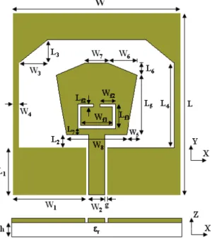
over UWB. A radiating tapered patch is placed inside polygon-slot as shown in Fig. 1.
Fig. 1. Geometry of the proposed UWB antenna.
A ‘C’ shaped slot is inserted in the radiating patch of antenna to avoid interference from WLAN
and HIPERLAN/2 bands as shown in Fig. 1. Since the slot is considered as half wave resonator,
of guided wavelength g, the slot resonates at notch frequency f0 and behaves as short circuit in
parallel to input impedance of the antenna. Hence, the antenna does not work in the frequencies
around f0 and it avoids the potential interference from WLAN band from 5.1 GHz to 5.9 GHz. Let, the
total length of C-slot [14] is denoted by Lslot and it is obtained by
0
2 1
2 2
g slot
r c L
f λ
ε
= =
+ (1)
where g is guided wavelength corresponding to notch frequency f0, c is velocity of light in free-space
and r is dielectric permittivity of FR4 substrate. Initially, C-slot is designed theoretically to resonate
at notch frequency f0 = 5.5 GHz to obtain total length of C-slot according to equation 1. In practice,
the notch frequency f0 = 5.5 GHz is obtained when the total length of C-slot is
Lslot = Wf1 + 2Wf2 + 2Lf1 + 2Lf2 as shown in Fig. 1 in the design of antenna structure with IE3D
electromagnetic solver. Hence, the length Lslot is practically equal to 0.6 g where
λ
g =λ
0ε
effandεeff =(εr +1)/2. Here, 0 is wavelength corresponding to the notch frequency f0 = 5.5 GHz, eff is
effective dielectric permittivity of dielectric substrate and r is dielectric permittivity of the substrate.
The proposed fabricated antenna with the total length of C-slot Lslot confirms the measured notched
frequency 5.5 GHz as shown in Fig. 2.
Fig. 2. Simulated and measured return losses Fig. 3. Photograph of the fabricated antenna.
of proposed antenna.
The antenna parameters are optimized based of method of moments based IE3d electromagnetic
optimizer. The optimized parameters of the proposed antenna are W = 29 mm, W1 = 12.65 mm, W2 =
2.8 mm, W3 = 5 mm, W4 = 1 mm, W5 = 1.75 mm, W6 = 5 mm, W7 = 4 mm, W8 = 10.5 mm, Wf1 =
5.5 mm, Wf2 = 2.75 mm, L = 31 mm, L1 = 8 mm, L2 = 2.2 mm, L3 = 4 mm, L4 = 4.5 mm, L5 = 10.25
mm, L6 = 2 mm, L7 = 1.1 mm, Lf1 = 4.2 mm, Lf2 = 0.5 mm, g = 0.45 mm. The fabricated antenna is
measured with Agilent E8362B network analyzer. The simulated and measured return loss curves of
return loss curves. The difference between them is mainly due to effect of soldering at SMA
connector and slight variation of dielectric permittivity, dissipation factor at high frequencies. The
antenna has impedance bandwidth of 3.1-10.6 GHz with a notched band from 5.1 GHz to 5.9 GHz.
The Fig. 2 shows that the measured UWB antenna has three resonating frequencies 3.8 GHz, 6.2 GHz
and 8.8 GHz. The photograph of fabricated antenna is shown in Fig. 3.
III. PARAMETRIC ANALYSIS
The effect of few sensitive parameters on the performance of antenna has been studied. The
analysis is done by changing one parameter, keeping all other parameters constant. IE3d simulator is
used in this analysis.
Fig. 4. Simulated return loss curves of antenna Fig. 5. Simulated return loss curves of antenna
for different intrusion depths L2. for different intrusion depths Lf1 of C-slot.
A. Effect of intrusion depth L2
The intrusion depth L2 affects impedance matching and bandwidth of antenna as shown in Fig. 4. It
causes more current distribution at bottom part of patch and top edge of ground plane as shown in
Fig. 9(a) when L2 is 2.2 mm. This parameter produces impedance mismatching when L2 changes from
2.2 mm. Hence, L2 is optimized to obtain better coupling from feed line to patch. The simulation
results show that the antenna has poor impedance matching at L2 = 1.2 mm. As L2 increases, the
second resonant frequency changes slightly. The first and third resonant frequencies shift left and
impedance bandwidth also varies. The antenna covers entire ultra-wide bandwidth at optimum value
L2 = 2.2 mm. Table I shows the effect of intrusion depth on simulated lower cut-off frequency flower,
upper cut-off frequency fupper and resonating frequencies. It is clear that fupper decreases and flower
remains constant with increase in L2. Hence, the impedance bandwidth decreases. The simulated
resonant frequencies also change.
B. Effect of length Lf1 of C-slot
If slot height Lf1 increases from 3.7 mm to 4.7 mm, the total length of C-slot increases. The notch
the fact that the length of slot Lslot is inversely proportional to notch frequency f0 of slot as mentioned
in equation 1. When Lf1 is 4.2 mm, the C-slot resonates at the notch frequency 5.5 GHz and WLAN
band is avoided due to abrupt change in impedance. As Lf1 varies from 4.2 mm, WLAN and
HIPERLAN/2 bands are not fully avoided as shown in Fig. 5. Hence, the notch frequency in WLAN
band is controlled by the slot height Lf1. Table II shows the effect of length Lf1 on simulated lower
cut-off frequency flower, upper cut-off frequency fupper, notch frequency f0 and notch bandwidth. As Lf1
increases, notch frequencydecreases and flower, fupper remain constant. The frequency range of notched-
band changes.
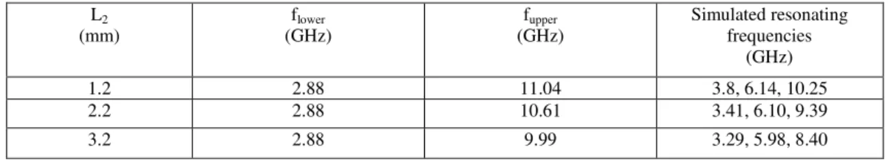
TABLE I. EFFECT OF L2 ON SIMULATED LOWER CUT-OFF FREQUENCY flower, UPPER CUT-OFF FREQUENCY fupperAND SIMULATED RESONANT FREQUENCIES
TABLE II. EFFECT OF Lf1 ON SIMULATED LOWER CUT-OFF FREQUENCY flower, UPPER-CUT OFF FREQUENCY fupperAND SIMULATED NOTCH FREQUENCY f0 AND SIMULATED NOTCH BANDWIDTH
Lf1
(mm)
flower
(GHz)
fupper
(GHz)
Notch frequency, f0 (GHz)
Simulated Notch Bandwidth
(GHz)
3.7 2.88 10.61 5.9 5.57-6.22
4.2 2.88 10.61 5.5 5.12-5.88
4.7 2.88 10.61 5.4 4.78-5.62
Fig. 6. Simulated return loss curves of antenna for different heights L3.
C. Effect of height L3 at upper part of ground plane
The influence of height L3 on resonant frequencies and bandwidth of antenna is observed. As L3
decreases from 7 mm to 1 mm, the value of second resonant frequency decreases as shown in Fig. 6.
L2
(mm)
flower
(GHz)
fupper
(GHz)
Simulated resonating frequencies
(GHz)
1.2 2.88 11.04 3.8, 6.14, 10.25
2.2 2.88 10.61 3.41, 6.10, 9.39
The impedance matching at second resonant frequency deteriorates. The impedance matching is better
at optimized value of L3 = 4 mm. Hence, this parameter plays important role in improving impedance
match around second resonant frequency.
(a) (b) (c) Fig. 7. Measured radiation patterns of proposed antenna in E-plane at (a) 3.8 GHz (b) 6.2 GHz (c) 8.8 GHz.
(a) (b) (c)
Fig. 8. Measured radiation patterns of proposed antenna in H-plane at (a) 3.8 GHz (b) 6.2 GHz (c) 8.8 GHz.
IV. RADIATION PATTERN AND CURRENT DISTRIBUTION
The radiation patterns are measured using anechoic chamber. Figs. 7, 8 present co-polarization,
cross polarization radiation patterns of the band-notched antenna in both E and H planes at measured
resonant frequencies 3.8 GHz, 6.2 GHz, 8.8 GHz. The antenna has figure of eight shaped radiation
patterns in E-plane which indicate that the antenna has bidirectional radiation patterns in this plane.
The antenna has stable omni directional radiation patterns in H plane except at 8.8 GHz. The radiation
pattern is slightly deviated from omni directional pattern in H-plane at 8.8 GHz. This is mainly due to
presence of higher order modes at higher frequencies.
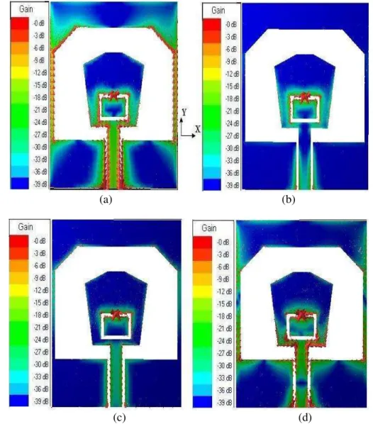
The radiation pattern relates to current distribution over entire operating band. Fig. 9 represents the
simulated current distribution at resonant frequencies 3.8 GHz, 5.5 GHz, 6.2 GHz and 8.8 GHz. At
3.8 GHz, the surface current distribution is mainly on feed line, lower portion of patch, outer edge of
patch and edges of the ground plane as shown in Fig. 9(a). Hence, these regions contribute more to
of C-slot and flows back to feeding cable as shown in Fig. 9(b). Hence, the high impedance at the slot
changes to nearly zero impedance at feed cable. Hence, there is abrupt change in impedance matching
and this impedance mismatch rejects WLAN band. At 6.2 GHz, the X-directed current distribution
produces cross polarization in H-plane.
(a) (b)
(c) (d)
Fig. 9. Surface current distribution on antenna at (a) 3.8 GHz (b) 5.5 GHz (c) 6.2 GHz (d) 8.8 GHz.
At 8.8 GHz, the cross polarization increases as shown in Fig. 8(c) because of presence of more X-
directed current components at lower part of patch and top edge of ground plane as observed in
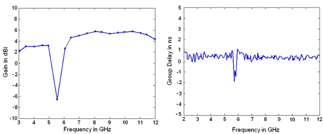
Fig. 9(d). Fig. 10 represents measured gain of antenna against frequency. The antenna has consistent
gain that changes from 2.1 dBi to 5.8 dBi in UWB except in notched band. There is sharp decrease of
gain around 5.5 GHz in notched band. This confirms rejection of WLAN and HIPERLAN/2 bands.
V. TIME DOMAIN ANALYSIS
Since group delay presents phase linearity in far-field, it is an important parameter in time domain.
Hence, group delay measurement is obtained by keeping two identical antennas at a distance of 20 cm
at far-field in face to face orientation. Fig. 11 shows the time domain group delay response. The graph
antenna has linear phase response and good pulse handling capability.
Fig. 10. Measured gain of proposed antenna. Fig. 11. Measured group delay of proposed antenna.
Since UWB antenna transmits pulse signals, the time domain characteristic of UWB antenna is
important. The UWB signal propagation is important for communications. To obtain the performance
of pulse transmission, two identical antennas are placed in face to face orientation, with a distance of
20 cm between them. The scattering transmission parameter S21 of antenna is measured and the
transfer function H( ) [15] of antenna is obtained from S21 as
( ) 2 21( )
j R c RcS e H
j ω
π ω
ω
ω
=
(2)
where c is velocity of light in free-space, R is distance between two identical antennas and is
angular frequency. The input pulse is Gaussian modulated cosine pulse with amplitude factor A = 1,
pulse width T = 200 picoseconds and centre frequency fc = 6.5 GHz. The time domain input
waveform i(t) is represented by
2
( )
( )
cos(2
).
tTc
i t
=
A
π
f t e
− (3)
The input waveform represented by equation 3 is shifted in time domain by 2.5 ns to avoid negative
time and is shown in Fig. 13. The normalized power spectral density (PSD) for indoor emission mask
is coded in matlab for input waveform mentioned in equation 3 with a time shift of 2.5 ns and is
presented in Fig. 12. The spectrum of input pulse satisfies UWB indoor emission mask specified by
FCC from 3.1 GHz to 10.6 GHz as shown in Fig. 12. The output waveform o(t) is computed by the
inverse Fourier Transform of product of H( ) and spectrum of input signal I( ) and is given by
o t
( )
−1(
H
( ). ( ))
ω
I
ω
=
F
(4)The time domain input and output pulses are displayed in Fig. 13. The slight ringing effect in
received pulse is mainly due to transmission characteristics of the system. The received waveform
indicates proper transient response for the proposed antenna. Hence, the antenna has good time
domain response and it can be used for UWB communications.
VI. CONCLUSION
A compact printed planar UWB slot antenna is presented with band-notched characteristic. The
desired notched band of 5.1-5.9 GHz is obtained by inserting C-slot in radiating patch to avoid
interference from WLAN and HIPERLAN/2 bands. The antenna operates from 3.1 GHz to 10.6 GHz,
except over notched band of 5.1-5.9 GHz. The radiation patterns are stable over UWB. The gain of
antenna is almost flat except in the notched band. The group delay of antenna indicates linear phase
response and good pulse handling capability. The antenna can be easily integrated with microwave
integrated circuits. The antenna is good for portable UWB systems.
ACKNOWLEDGMENT
The authors would like to express sincere gratitude to the scientist, U. S. Pandey, for providing
measurement facilities in LRDE lab at Defence Research Development Organisation (DRDO),
Bangalore, Govt. of India.
REFERENCES
[1] A. Mehdipour, K. M. Aghdam, R. F. Dana, and M. R. K. Khatib, “A novel coplanar waveguide-fed slot antenna for
ultrawideband applications,” IEEE Trans. Antennas Propag., vol. 56, no. 12, pp. 3857–3862, Dec. 2008.
[2] N. Farrokh-Heshmat, J. Nourinia, and C. Ghobadi, “Band-notched ultra-wideband printed open-slot antenna using variable on-ground slits,” Electron. Lett., vol. 45, no. 21, pp. 1060–1061, Oct. 2009.
[3] A. Subbarao and S. Raghavan, “A compact UWB Slot antenna with signal rejection in 5-6 GHz band”, Microw. Opt.
Technol. Lett., vol. 54, no. 5, pp. 1292–1296, May 2012.
[4] K. Chung, S. Hong, and J. Choi, “Ultrawide-band printed monopole antenna with band-notch filters,” IET Microw. Antennas Propag., vol. 1, no. 2, pp. 518–522, Apr. 2007.
[5] B. Ahmadi and R. Faraji dana, “A miniaturised monopole antenna for ultra-wide band applications with band-notch filter,” IET Microw. Antennas Propag., Vol. 3, no. 8, pp. 1224–1231, Feb. 2009.
[6] K. Song, Y. Z. Yin, and L. Zhang, “A novel monopole antenna with a self-similar slot for wideband applications,”
Microw. Opt. Technol. Lett., vol. 52, no. 1, pp. 95-97, Jan. 2010.
[7] Y. L. Zhao, Y. C. Jiao, G. Zhao, L. Zhang, Y. Song, and Z. B. Wong, “Compact planar monopole UWB antenna with
band-notched characteristic,” Microw. Opt. Technol. Lett., vol. 50, no. 10, pp. 2656–2658, Oct. 2008.
[8] K. Yin and J. P. Xu, “Compact ultra-wideband antenna with dual bandstop characteristic,” Electron. Lett., vol. 44, no. 7, pp. 453–454, Mar. 2008.
[9] M. Abdollahvand, G. Dadashzadeh, and D. Mostafa, “Compact dual band-notched printed monopole antenna for UWB
[10] C. Y. Hong, C. W. Ling, I. Y. Tarn, and S. J. Chung, “Design of a planar ultrawideband antenna with a new band-notch structure,” IEEE Trans. Antennas Propag., vol. 55, no. 12, pp. 3391–3397, Dec. 2007.
[11] M. Abdollahvand, G. R. Dadashzadeh, and H. Ebrahimian, “Compact band-rejection printed monopole antenna for UWB application,” IEICE Electron. Exp., vol. 8, no. 7, pp. 423–428, Apr. 2011.
[12] A. M. Abbosh and M. E. Bialkowski, “Design of UWB planar band notched antenna using parasitic elements,” IEEE
Trans. Antennas Propag., vol. 57, no. 3, pp. 796–799, Mar. 2009.
[13] L. H. Ye and Q. X. Chu, “Improved band-notched UWB slot antenna,” Electron. Lett., vol. 45, no. 25, pp. 1283-1285, Dec. 2009.
[14] T. Dissanayake and K. P. Esselle, “Prediction of notch frequency of slot loaded printed UWB antennas,” IEEE Trans. Antennas Propag., vol. 55, no. 11, pp. 3320–3325, Nov. 2007.
[15] V. A. Shameena, S. Mridula, A. Pradeep, S. Jacob, A. O. Lindo, and P. Mohanan, “A compact CPW fed slot antenna