Abstract— A novel FSS-Backed reflectarray unit cell is introduced to design a dual-band X/Ku Reflectarray Antenna (RA). A Ku-band RA based on this FSS-Backed cell element is designed and located on the top of a conventional X-band RA. Actually, the band-stop Frequency Selective Surface (FSS) property is applied to a wideband element to create isolation between X and Ku band RAs which utilizing the same radiating element. A wideband cell element with attached quasi-spiral phase delay line is employed for phase compensation in both bands. As a FSS-backed cell element, the remarkable feature of the proposed dual band unit cell compared to previous works is its possibility of operation in closer frequency bands in comparison with other dual band FSS-backed RAs. Two reflectarrays with aperture size of 7.65λ×7.65λ and 7.35λ×7.35λ are designed, fabricated and measured for X band and Ku band, respectively. Measured results show 1-dB gain bandwidth of 12% for X band and 11% for Ku band which demonstrate wideband operation of this dual-band reflectarray antenna.
Index Terms— Delay line, dual band, FSS-Backed reflectarray antenna,
quasi-spiral.
I. INTRODUCTION
Reflectarray antennas compared to other high gain antennas are used extensively in some long
distance communication systems, due to their numerous advantages. Nowadays, these antennas are
applicable for dual-band applications. If frequency bands are chosen close to each other, a single layer
dual-band reflectarray antenna can be used [1]-[3]. Compared to multi-layer structures, this technique
leads to reduction of the antenna’s volume, but because of increasing mutual coupling between both
the elements for different bands, the design would be difficult. To achieve operational bands
considerably at a great distance, design in multi-layer configuration is preferred occasionally [4]-[6].
However, employing multi-layer configuration causes some restrictions in selecting thickness of
substrates and the elements type as well as complexity of fabrication process.
In [7] a new type of reflectarray antennas (FSS-Backed reflectarray) for multi-band applications is
introduced. Due to more degrees of freedom for design and good isolation between both band
elements without any limitations in selection of thickness of substrates and type of elements, this type
of antenna is preferred to the previous mentioned ones in some applications. Recently, some attempts
have been done to employ these antennas for dual-band purposes [8]-[10]. In these structures,
Dual-band X/Ku Reflectarray Antenna Using
a Novel FSS-Backed Unit-Cell with
Quasi-Spiral Phase Delay Line
Iman Derafshi, Nader Komjani, Ensieh Ghasemi-Mizuji and Mohammad Mohammadirad,
Department of Electrical Engineering, Iran University of Science and Technology, Tehran 1684613114, Iran, e-mail: [email protected],[email protected] , [email protected],
variable-size element technique is usually applied for compensation of spatially phase error of
incoming wave. It is worth mentioning that by using the FSSs introduced in [7]-[9] designing dual
band reflectarray in the frequency bands which are close to each other is not possible.In other words,
obtaining reflection and transmission properties for two close wide bands would not be achievable
with the elements introduced in the above literature.
In this paper, two RAs are designed and fabricated for dual band operation in X and Ku band. Both
RAs are exploiting an element with attached phase delay lines as the main radiating element while a
double layer FSS element is added beneath the Ku-band (17-19 GHz) element to obtain transmission
property in X-band (8-9 GHz) and simultaneously simulating the ground plane in Ku band.By virtue
of this structure, designing two stacked RA for closer frequency bands in comparison with the other
dual band FSS-backed RAs will be possible which has not been previously reported. Thanks to the
linear phase response of the delay line method [11]-[13] and it’s lower tolerance in manufacturing. It
has been used as the phase shifting mechanism for main element of the designed RAs in this work. As
mentioned above a wideband element based on quasi-spiral phase delay line is utilized for designing a
FSS-backed reflectarray. In fact, the FSS layer is considered as ground plane for the top Ku-band and
also as atransparent layer for the bottom X-band RA.
II. ANTENNA CONFIGURATION
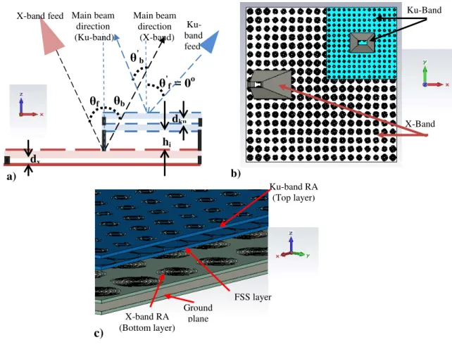
Fig. 1 shows the schematic view of the proposed dual band RA. As it is depicted in Fig. 1(a), the
FSS-Backed reflectarray antenna for Ku band is placed on the top of X band conventional reflectarray
by a (hi=1 cm) spacer. It is to be noted that all the dimensions for spacers were chosen based on
achievable mechanical accuracy and material availability. The design has been carried out so that the
center-fed (θ′f=0 o, ϕ′
f=0 o
)FSS-backed Ku-band reflectarray antenna and -15o (θf=15 o, ϕ
f=180 o
)
offset-fed X-band RA produce -15o (θ′b=15 o, ϕ′
b=180 o
) and 15o (θb=15 o, ϕ
b=0 o
) off-broadside beams in
elevation plane, respectively.
In Fig. 1(b) we can see the location of the Ku-band RA on top of the X-band RA and compare its
size with the bottom RA. The size of this Ku-band FSS-Backed RA is about ¼ of the X-band one.
According to Fig. 1(c), the FSS-backed RA is composed of two layers. The phasing elements are
etched on the top surface of the upper layer and FSS elements are printed on both sides of the bottom
layer, where the free space distance between these two layers (dku) is 2 mm. Also, as can be seen in
Fig. 1(c) the X-band elements are etched on top of the bottom layer which is backed by a ground
plane at distance of 2 mm (dx) to increase the bandwidth. All the used substrates in this design are
RO-4003 with thickness 32 mil.
A. Design of Ku band element
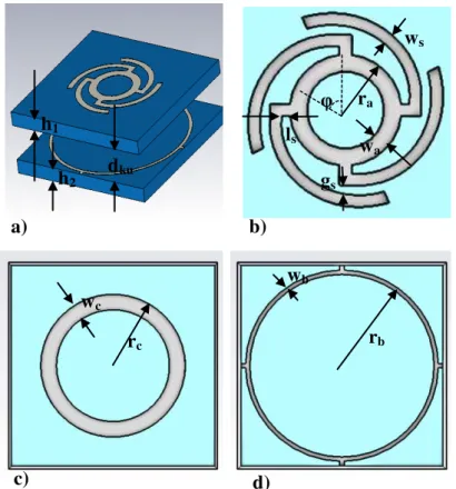
The unit-cell configuration for Ku-band is shown in Fig. 2. As it can be seen from Fig. 2(a), this
element consists of two RO-4003 substrates separated by a 2 mm spacer (dku) from each other. The
the top of the upper substrate [14]. The elements of Fig. 2(c) and Fig. 2(d) printed on both sides of the
bottom substrate are used as FSS layer (Fig. 3(a)).The main effect of 2 mm spacer is to reduce the
coupling between the elements on top (radiating) and bottom (FSS) layers and thus increasing the
bandwidth of the RA [15]. Final dimension of the unit cell is 9 mm×9 mm.The design process of the
proposed cell element is originated from the method presented in [7] for multiband-multi polarization
elements. As the starting point, the dimensions of the FSS layer are maintained while the length of the
phase delay lines of the radiating element is changed to achieve a large phase variation range. Then,
the FSS layer is adjusted to obtain maximum reflection in Ku band and at the same time minimum
transmission in X-band.
Fig. 1. a) Side view, b) top view and c) 3D view.
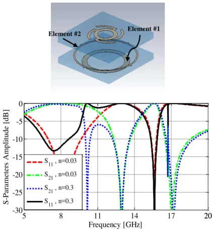
Based on the method in [7] two different FSS-backed unit cells are studied to get more insight on
the cell element of Fig. 2. As shown in Fig. 3, first element consists of a phasing element on top layer
and a ring element on bottom layer as the FSS-layer, for frequency range of 17.5 GHz. The plot of
Fig. 3 illustrates the reflection coefficient for extreme values of n, where n indicates the numbers of
turn (n=1 equals to a full turn (360o)). The amplitude of reflection in 16.5-18.5 GHz band is greater
than -1 dB (%80 of reflection) which demonstrates that the FSS layer acts as a ground plane to some
extent. On the other hand, the out of band performance of this element shows that: 1) most of the
incident wave is transmitted at frequencies which are far enough from the aforementioned band. 2)
θ
'f
= 0
oKu-band feed
θf
θb
X-band feed
dx
hi
θ
'b
a)
Main beam direction (X-band) Main beam
direction (Ku-band)
dku
Ku-Band
X-Band
b)
Ku-band RA (Top layer)
FSS layer Ground
plane X-band RA
(Bottom layer)
Also, the magnitude of reflection coefficient for large values of n shows that about 25% of the
incident wave will be reflected in the frequency range of 7.5-9 GHz by this element. It is to be noted
that to achieve a FSS-backed element where in the pass-band and stop-band occurs close to each
other, it is necessary to decrease the amount of the latter reflection.
Fig. 2. a) Schematic view of the proposedunit cell. b) Phasing element c) FSS element on bottom, d) FSS element on top.
Therefore, the element of Fig. 4 is used to obtain more reduction of the reflection coefficient in out
of band, particularly at frequencies close to the design frequency. Similar to [16], the ring element of
the FSS layer is connected to the adjacent elements by four stubs. According to [17], these additional
stubs cause some reduction of the inductance in equivalent circuit of FSS element. On the other side,
to maintain the resonance frequency, fr= , the capacitance in the equivalent circuit should be
increased. Since the bandwidth of stop-band filters is proportional to , the stop band around 17.5
GHz will increase while the reflection coefficient out of the operational band (around 8 GHz) will
decrease to -7 dB, as is shown in Fig. 4.
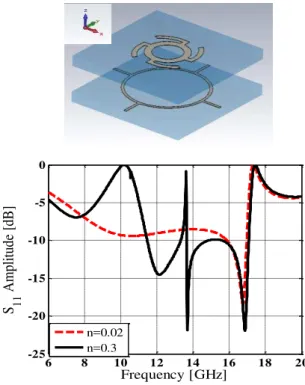
Based on the above investigation to achieve an appropriate performance in both bands, the FSS
element in Fig. 5 is exploited which is a combination of both typical and modified elements in Fig. 3
and Fig. 4. The dimensions of the elements are optimized to attain proper operation in both bands
(7.5-9 GHz and 17.2-18.2 GHz). The amplitude of the reflected wave for two different values of n
(S11) is shown in Fig. 5. As it is observed in this figure the amplitude of S11 is less than -9 dB in the
frequency range of 7.5-9 GHz and in Ku band (17.2-18.2 GHz) S11 amplitude is more than -0.8 dB.
Therefore, the goal is obtained. The final design parameters are as follow: wb =0.2 mm, rb =4.3 mm,
r
aw
al
sw
sg
sr
bw
br
cw
ch
1h
2d
kuφ
b)
a)
wc =0.7 mm, rc=3.2 mm.
Fig. 3. FSS-backed element with a ring as FSS layer.
Fig. 4. FSS-backed element with a stub-loaded ring as FSS layer.
The phasing element of FSS-Backed RA (the upper layer in Fig. 2(a)) is a ring with four attached
delay lines. Note that the phase shift is proportional to twice of the electric length of phase delay line
[18]. Therefore, by varying the delay line length the necessary phase shift is attained. Note that the
variable parameter of the phasing element is the turn value; therefore it is worthwhile to obtain the
relation between the turn value and length of the delay line. The equation of the radius versus φ for
spiral line is expressed by (1):
5 8 11 14 17 20
-12 -10 -8 -6 -4 -2 0
Frequency [GHz]
S 1
1
A
m
pl
it
ude
[
dB
]
n= 0.02 n= 0.3
6 8 10 12 14 16 18 20
-25 -20 -15 -10 -5 0
Frequency [GHz]
S 11
A
m
pl
it
ude
[
dB
]
2
(
) (
)
a s s s
r
r
l
g
w
(1)Where the parameters φ, ws, gs, ls and raare specified in Fig. 2(b). By substituting φ = 2nπ in (1):
4 (
)
a s s s
r
r
l
n g
w
(2)Where n is denoting the number of turn. The differential equation shown below can be considered:
. 2 .
dl r d
r dn (3)By integrating and simplifying the formula, (4) is derived.
2
[
a s2 (
s s)]
l
n
r
l
n g
w
(4)The parameters gs and ws are optimized to obtain maximum matching with ring at 17.5 GHz and the
resonance dimensions of ring are designed in center frequency. The optimum parameters are obtained
as: ws= 0.35 mm, gs= 0.2625 mm, ls= 0.2 mm, ra= 1.58 mm, wa= 0.5 mm.
Fig. 5. The proposedFSS-backed reflectarray unit cell and its reflection response.
To check the operation of FSS for different values of phase delay lines length, the S-parameters are
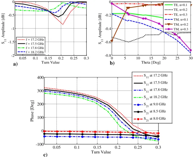
obtained using CST Microwave Studio. Fig. 6(a) shows the amplitude of S11 versus values of turn. As
it is observed, at 17.5GHz the amplitude of reflection for a range of delay lines length is above
-0.55dB. Also, the amplitude of reflected wave in Ku-band which is shown in Fig. 6(a) for several
frequencies, demonstrates the ground plane role of FSS layer in Ku-band.
To get a better understanding, the performance of this unit cell in X band is examined. The S11
parameter versus different turn values of phase delay line is presented in Fig. 6(b). In the X band (8-9
5 8 11 14 17 2020
-30 -25 -20 -15 -10 -5 0
Frequency [GHz]
S
-P
a
ra
m
e
te
rs
A
m
pl
it
ude
[
dB
]
S
11 , n=0.03
S
21 , n=0.03
S
21 , n=0.3
S
11 , n=0.3
GHz) and for various lengths of delay lines, |S11| is under -9dB which means that the FSS-Backed
RA transmits the incident wave completely in this frequency band.
The reflection phase of the FSS-backed cell element versus delay line length is depicted in Fig
.6(c). The phase response curves in Fig. 6(c) are parallel to each other for various frequencies which
demonstrate wideband performance of this element. A phase shift range of 360o for reflectarray is
achieved for variation of n=0.02 to 0.3.
Since the Ku-band FSS-Backed RA occupies ¼ of the X band RA surface, our expectation would
be a negligible variation of the transmission phase. The phase curves of Fig .6(c) demonstrate this
transparency in X-band.
0.05 0.1 0.15 0.2 0.25 0.3
-2 -1.5 -1 -0.5 0 Turn Value S 1 1 A m pl it ude [ dB ]
f = 17.2 GHz f = 17.5 GHz f = 17.8 GHz f = 18.2 GHz
0 5 10 15 20 25 30
-0.8 -0.6 -0.4 -0.2 0 Theta [Deg] S 1 1 A m pl it ude [ dB ] TE, n=0.1 TE, n=0.2 TE, n=0.3 TM, n=0.1 TM, n=0.2 TM, n=0.3
0.05 0.1 0.15 0.2 0.25 0.3
-100 0 100 200 300 400 Turn Value P ha se [ D eg]
S11 at 17.2 GHz
S
11 at 17.5 GHz S11 at 17.8 GHz
S
11 at 18.2 GHz S
21 at 9.0 GHz S
21 at 8.5 GHz S
21 at 8.0 GHz
Fig. 6. S11 amplitude versus turn value for (a) X-band and (b)Ku-band FSS-Backed unit cell. c) S11and S21phase versus
values of turn for different frequencies.
Fig. 7(a) and. 7(b) show the effect of incidence angle (for Ku-band horn) on phase and amplitude
response of the elementin Fig. 5. It should be mentioned that the reflection coefficient is greater than
-0.8dB for the maximum turn value and at the angles of incidence up to θ=30o. Furthermore, the
magnitude of transmission coefficient for various turn values and TE/TM waves at different angles of
incidence (for band horn) demonstrate the low sensitivity of the proposed unit-cell to position
X-band feed.
b)
a)
0 5 10 15 20 25 30 -150 -100 -50 0 50 100 150 Theta [Deg] S 1 1 P ha se [ D e g] TE, n=0.1 TE, n=0.2 TE, n=0.3 TM, n=0.1 TM, n=0.2 TM, n=0.3
0 5 10 15 20 25 30
-0.8 -0.6 -0.4 -0.2 0 Theta [Deg] S 1 1 A m pl it ude [ dB ] TE, n=0.1 TE, n=0.2 TE, n=0.3 TM, n=0.1 TM, n=0.2 TM, n=0.3
0 5 10 15 20 25 30
-0.5 -0.4 -0.3 -0.2 -0.1 0 Theta [Deg] S 2 1 A m pl it ude [ dB ]
TE , n=0.1 TE , n=0.2 TE , n=0.3 TM , n=0.1 TM , n=0.2 TM , n=0.3
Fig. 7. S11 a) phase versus incident wave angle at 17.5.GHz. b) amplitude versus incident wave angle at 17.5.GHz. c) S21
amplitude versus incident wave angle at 8GHz. B. Design of Ku band reflectarray
The back-scattered field of the whole reflectarray in an arbitrary direction (u) is expressed as:
0 0 0
1 1
ˆ
( )
(
.
) (
. ) ( . ).exp(
[|
|
. ]
)
Q P
pq f pq pq f pq pq
p q
E u
F r
r
A r
u A u u
jk
r
r
r
u
j
(5)Where F and A are feed antenna pattern and unit cell element pattern, respectively. rpq and rf denote
the position vector to pqth element and the position of the feed antenna, respectively. Also, u0 is the
chosen main beam direction and φpq is the required phase shift at pqth element which is given as:
0[ ( cos sin ) sin ]
pq k dpq xpq b ypq b b
(6)Where k0 is the free space wave number. And (xpq ,ypq) is the coordinate of pqth element and (θb ,φb)
is the main beam direction [18].
A 14×14 element center fed FSS-Backed reflectarray is designed and fabricated using cell element
of Fig. 2. The reflectarray aperture is illuminated by a horn antenna with F/D=1.38. The RA was
designed to produce a main beam at (15o, 180o).
The required phase shift distribution on the surface of Ku band RA is depicted in Fig. 8. The delay
line length for producing the phase shift in Ku band has been calculated from Fig. 6(c).
The fabricated RA antenna is shown in Fig. 9. As aforementioned, this antenna consists of two
layers with distance of 2 mm from each other (Fig. 9(d)). The top view of the upper layer, the top
a)
b)
view of the bottom layer and the back view of the bottom layer of Ku band RA are demonstrated in
Fig. 9(a), 9(b) and 9(c), respectively.
Fig. 8.The required phase shift for each element of FSS-Backed RA (Ku-band).
Fig. 9. a) top view of FSS-Backed RA, b) top view of FSS layer, c) back view of FSS layer and d) side view of FSS-Backed RA where placed on top of X-band RA.
The measurement setup is shown in Fig. 10. The measured radiation pattern at 17.5 GHz and the
gain curve are represented in Fig. 11. As it is observed the main beam direction in E-plane is -15 deg
off-broadside and the measured gain is 23.9 dBi (aperture efficiency is 36%) at 17.5 GHz. The
measured 3-dB beam width and side lobe level are 6o and -15dB, respectively. Fig. 11(b) illustrates
the measured gain versus frequency for the frequency range of 16-19 GHz, where the frequency range
of 16.5-18.5 GHz is measured as 1-dB gain bandwidth. It can be seen that the peak gain occurs at a
lower frequency with regard to design frequency, which can be due to fabrication tolerances.
-0.06 -0.04 -0.02 0 0.02 0.04 0.06
-0.06
-0.04
-0.02
0
0.02
0.04
0.06
50 100 150 200 250 300 350
b)
a)
Fig. 10. The test setup of the mentioned FSS-Backed RA.
40 60 80 100 120
-25 -20 -15 -10 -5 0
Azimuth[Deg]
N
or
m
a
li
z
e
d
P
a
tt
e
rn
[dB
]
f=17.5 GHz
16 16.5 17 17.5 18 18.5 19
16 18 20 22 24
frequency [GHz}
G
a
in
[dB
]
Fig. 11 .a) Normalized pattern of FSS-Backed RA at 17.5 GHz. b) Gain versus frequency FSS-Backed RA.
C. The effect of FSS-backed RA on the performance of the X band RA
Eventually, the performance of the X-band RA is assessed in the presence of Ku band FSS-backed
RA. The unit cell of X-band RA is shown in Fig. 12. This wideband element has been previously
introduced by the authors [14], and to avoid redundancy is not repeated here.
Fig. 12. a) Unit cell element of X band RA and b) Prototype of fabriceted X band RA.
Based on [9] the larger spacing between two arrays results in smaller coupling. However, because
of some restrictions on facilities this space was chosen to be 1 cm. Utilizing the cell element in [14],
Fig. 12(a), a 18×18 element reflectarray was designed and fabricated for X-band, Fig. 12(b), to
a)
b)
30 45 60 75 90 105 120 135 150 165 180 5
10 15 20 25
Azimuth [Deg]
R
adi
at
ion
pa
tt
er
n
[dB
] without ku band
with ku band
8 8.5 9 9.5 10
0 5 10 15 20 25
Frequency(GHz)
G
ai
n
(dB
)
Without ku band With ku band
produce a main beam in direction of (15o,0o). It should be noted that a -15deg offset feed horn was
used to illuminate this RA with F/D=1.21.
As it was shown in Fig. 7(c) the performance of FSS-backed RA has low sensitivity to the X-band
horn and its angle of illumination. Therefore, it is expected that the location of FSS-backed RA on top
of the X-band RA has negligible effect on performance of the X-band RA. However, to achieve more
mechanical strength it was preferred to place it at the corner, as shown in Fig. 13(a).
The radiation pattern at 8.5GHz and gain curve vs. frequency for X-band RA are presented in Fig.
13(b) and .13(c). As it can be seen these results are given with and without Ku-band RA. Separately
measurement of X-band RA shows the efficiency of the single X-band RA at 8 GHz is about 63% (̴ 26.12 dB gain) while it is reduced to 59% (̴ 26.4 dB gain) at the frequency of 8.5 GHz. However,
when Ku-band RA is located on the top of the X band RA, the maximum gain at 8 GHz is reduced to
24.68 dB (̴ 44% efficiency) and 24.75 dB gain (̴ 40% efficiency) at 8.5 GHz. Therefore, we can conclude an insertion loss of about 1.5 dB and 1.65 dB for the frequencies of 8 GHz and 8.5 GHz
respectively. Also, According to this figure, the insertion loss is increased as the frequency increases.
The 1-dB gain bandwidth for X band RA with Ku band RA is about 12%.
Fig.13.a) Prototype of fabricated dual band RA, b) Gain versus frequency for X band RA with and without Ku-band FSS-Backed RA and c) Radiation pattern X band RA with and without Ku band FSS-FSS-Backed RA.
III. CONCLUSION
In this study a (X/Ku) dual band reflectarray antenna was fabricated and measured. A new element
consisted of a ring with four quasi-spiral delay lines was utilized as the unit cell element. Moreover,
two FSSs were used to isolate the two bands. The FSS insertion loss is about 1.6 dB in X band. The
measurements show the proper operation in both frequency bands. In addition, the efficiency in X
band and Ku band are 40% and 36%, respectively. The 1-dB gain bandwidth for X band in presence
a)
b)
of Ku band is about 12% and for Ku band is 11%.
REFERENCES
[1] M. R. Chaharmir, J. Shaker, N. Gagnon, and D. Lee, “Design of broadband, single layer dual-band large reflectarray
using multi open loop elements,” IEEE Trans. Antenna Propag.,vol. 58, no. 9, pp. 2875-2883, Sep. 2010.
[2] M. R. Chaharmir, J. Shaker, and N. Gagnon, “Broadband dual-band linear orthogonal polarization reflectarray,” Electron. Lett.,vol. 45, no. 1, Jan. 2009.
[3] H. Hasani, and C. Piexeiro, “Dual-band, dual-polarized microstrip reflectarray antenna in Ku band,” Loughborough Antennas & Propagation Conference. Nov. 2012.
[4] C. Han, J. Huang, and K. Chang, “A high efficiency offset-fed X/Ka-dual-band reflectarray using thin membranes,” IEEE Trans. Antenna Propag.,vol. 53, no. 9, pp. 2792-2798, Sep. 2005.
[5] C. Han, Ch. Rodenbeck, J. Huang, and K. Chang, “A C/Ka dual frequency dual-layer circularly polarized antenna with
microstrip ring elements,” IEEE Trans. Antenna Propag., vol. 52, no. 11, pp. 2871-2876, Nov. 2004.
[6] M. R. Chaharmir, J. Shaker, and M. Cuhaci, “Development of dual-band circularly polarized reflectarray,” IEE Proceeding-Microwaves Antenna and Propagation, vol. 153, no. 1, pp. 49-54, Feb. 2006.
[7] J. Shaker, and M. Cuhaci, “Multi-band, multi-polarisation reflector-reflectarray antenna with simplified feed system
and mutually independent radiation patterns,” IEE Proceeding-Microwaves Antenna and Propagation, vol. 56, no. 12, pp. 3700-3706, Dec. 2008.
[8] M. R. Chaharmir, J. Shaker, and H. Legay, “Dual-band Ka/X reflectarray with broadband loop elements,” IET Microw. Antenna Propag.,vol. 4, lss. 2, pp. 225-231, 2010.
[9] L. Li, Q. Chen, Q. Yuan, k. Sawaya, T. Maruyama, T.Furuno and Sh. Uebayashi, “Frequency selective reflectarray using crossed-dipole elements with square loops for wireless communication applications,” IEEE Trans. Antenna Propag.,vol. 59, no. 1, pp. 89-99, Jan. 2011.
[10]Y. Chen, L. Chen, H. Wang, X. Gu and X. Shi, “Dual-band crossed-dipole reflectarray with dual-Band frequency
selective surface,” IEEE Antenna Wireless Propag .Lett, vol. 12, pp. 1157-1160, 2013.
[11]R. D. Javor, X. Wu, and K. Chang, “Design and performance of a microstrip reflectarray antenna,” IEEE Trans. Antenna Propag., vol. 43, no. 9, pp. 932-939, Sep. 1995.
[12]H. Hasani, M. Kamyab, and A. Mirkamali, “Broadband reflectarray antenna incorporating disk elements with attached phase-delay line,” IEEE Antenna Wireless Propag. Lett, vol. 9, pp. 156-158, 2010.
[13]R. Sh. Malfajani, and Z. Atlasbaf, “Design and implementation of a broadband single layer circularly polarized
reflectarray antenna,” IEEE Antenna Wireless Propag.Lett, vol. 11, pp. 973-976, 2012.
[14]I .Derafshi, N. Komjani and M. Mohammadirad, “A Single Layer Broadband Reflectarray Antenna by Using
Quasi-spiral Phase Delay Line,” IEEE AWPL,vol. 14, pp. 84-87, 2014.
[15]M. Mohammadirad, N. Komjani, M. Chaharmir, J. Shaker, A. Sebak, ”Phase Error Analysis of the Effect of Feed Movement on Bandwidth Performance of a Broadband X-Ku Band Reflectarray,” International Journal of RF and Microwave Computer-Aided Engineering/Vol. 23, No. 5, pp.17-526, 2012.
[16]J. Li, Q. Chen, Q. Yuan, and K. Sawaya, “FSS sandwiched reflectarray for dual–frequency application,”Microwave Conference Proceedings (APMC), Asia-Pacif1ic. pp. 877 – 880, 2010.


![Fig. 10. The test setup of the mentioned FSS-Backed RA. 40 60 80 100 120-25-20-15-10-50 Azimuth[Deg]Normalized Pattern [dB] f=17.5 GHz 16 16.5 17 17.5 18 18.5 191618202224frequency [GHz}Gain [dB]](https://thumb-eu.123doks.com/thumbv2/123dok_br/18888158.424330/10.892.237.673.107.392/setup-mentioned-backed-azimuth-normalized-pattern-frequency-gain.webp)
