*e-mail: [email protected], [email protected]
1. Introduction
The ferromagnetic microwires have been recognized as promising materials for small-size magnetic sensors in recent years. The giant magneto-impedance (GMI) effect of these wires which used for weak-ield detection and high-resolution sensors has been attracted much attentions1-3.
Many previous works focused on annealing treatment for improving the GMI ratio and ield response sensitivity of the microwires simultaneously by releasing the residual inner stress of an as-quenched microwire which enhances the circumferential permeability μφ, such as joule heat-treatment
and stress annealing4-8. Based on the deinition of GMI ratio, ΔZ∕Z0(%)=((Z(Hex)-Z(H0))∕Z(H0)×100%, reducing Z0
is an immediate method to enhance the GMI ratio through annealing treatment while increase the Zmax or keep it unchanged. The complex impedance Z can be expressed as
Z(H0)=R(H0)+iX(H0), where R(H0) and X(H0) are the resistance and the reactance at zero external ield, respectively. In this case, the reducing R(H0) and X(H0) simultaneously is favor of obtaining high GMI performance.
Another important factor for the wires used as practical GMI magnetic sensors is the ield response range. In fact, the enhancement of GMI for the microwire is generally at the expense of enhancing its response ield range thus reducing its ield response sensitivity (ξ). The conlict limits the applications of GMI microwires on miniature sensors to some extent. Herein, for resolving this issue, i.e, obtaining
high GMI ratio with broad response ield concurrently, new tailoring techniques is necessary.
The origin of large GMI ratio is ascribed to the skin effect with small penetration depth δ, small Rdc and large circumferential permeability μφ, which is closely related to the microwires with ine surface and roundness1. It is well
known that the melt-extraction technique with high cooling rate and process conveniently controlled (i.e. linear velocity of wheel, feed rate of the molten) can produce micorowires of uniform diameter and roundness which has excellent GMI microwires9,10. In our present work, compared with
conventional Joule annealing (JA), we have induced a cryogenic Joule annealing (CJA) under larger amplitude current across the melt-extracted Co68.15Fe4.35Si12.25B13.25N b1Cu1 amorphous microwire for effectively improving its anisotropy ield and keep the regular outer-shell amorphous structure with characterizing the transformation of static domain structure (SDS) under large DC currents11.
2. Experiments
We have fabricated soft magnetic amorphous microwires of Co68.15Fe4.35Si12.25B13.25Nb1Cu1 with diameter of 35 μm by a modiied melt-extracted technique and employed by CJA technique9. Impedance measurements are carried out at the
intermediate frequency range of 100 kHz~15 MHz using Agilent 4294A precision impedance analyzer. The samples with 18 mm length were subject to current annealing with
Domain Transformation and MI of Melt-extracted Co
68.15Fe
4.35Si
12.25B
13.25Nb
1Cu
1Microwires
by Cryogenic Joule Annealing
Dawei Xinga, Dongming Chena, Jingshun Liub, Lunyong Zhangc,
Hongexian Shena, Fang Liua, Jianfei Suna*
aSchool of Materials Science and Engineering, Harbin Institute of Technology, 92,
West Dazhi St, Harbin, Heilongjiang, China
bSchool of Materials Science and Engineering, Inner Mongolia University of Technology,
Hohhot 010051, China
cMaxPlank Center of Complex Phase Materials, Pohang University of Science and Technology,
Pohang 790-784, Republic of Korea
Received: September 10, 2014; Revised: August 24, 2015
Giant magneto-impedance (GMI) effect and domain transformation for melt-extracted Co68.15 Fe4.35Si12.25B13.25Nb1Cu1 amorphous wires have been induced by a cryogenic Joule annealing (CJA) treatment with different DC current amplitude (0~350 mA) for 240s. Experimental results indicate that the maximum GMI ratio ([ΔΖ∕Ζ0]max) achieves to 188.1% with exciting ield increasing to 1.8 Oe
monotonically for 300 mA annealing treated wires, which can attribute to the surface complex domain structure change formed by CJA treatment. The liquid nitrogen can protect the wire from crystallization when applied large DC currents. Moreover, the CJA treatment can improve the response sensitivities effectively. These remarkable characteristics make the melt-extracted microwires by CJA tailoring as the promising candidate material for small-sized magnetic sensors.
current rang of 0~350 mA for 240 seconds and their MI properties were measured by 20 mA driving amplitude with an external magnetic ield applied along the axial direction of the microwire. The GMI ratio of the wire is deined as: ΔZ∕Z0=((Z(H)-Z(H0))∕Z(H0)×100%, and the ield
response sensitivity is deined as: ξ=Δ(ΔZ∕Z0)∕ΔHex×100%. The observation of domain structures of the microwires was performed by a Nanoscope III multimode atomic force microscope from Digital Instruments. A Veeco micro-etched silicon probe tip is used to collect related information by applying a combination of tapping and lift mode. During lift mode, the magnetic data were collected and displayed. Selected lift height range is 100 nm. Liquid nitrogen was adopted to hinder the evolution of circumferential domain and protect the microwires against crystallization.
3. Results and Discussion
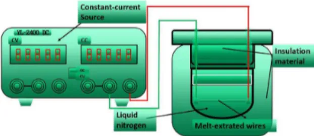
Figure 1 displays the CJA device schematically. This method is designed to cool the surface of microwire by immersing into liquid nitrogen medium and to prevent the microwire from oxidation or over-heating with applying the magnetic and stress anisotropy to alter intrinsic anisotropy ield. In the CJA process, the microwire is surrounded by nitrogen gas. The excessively large Joule heat is conducted out by the nitrogen gas shell with low temperature role rendering the microwire crystallization process which obviously damages the GMI properties.
The ields dependence of GMI ratios (ΔZ/Z0) for CJA-ed microwires with selected annealing currents in range of 0~350 mA and frequencies of 100 KHz ~ 10 MHz are illustrated in Figure 2. For the as-cast state in Figure 2a, all the ΔZ/Z0 curves without any rising peak decrease when the applied ields increase at all frequencies, indicating small circumferential anisotropy. After 200 mA current annealing, the rising peaks of GMI curves appear and the positions of the peaks monotonically increase with the frequencies increase ranging from 10 KHz to 20 MHz. At 10 MHz, the linear response ield Hp is 0.8 Oe with the (ΔZ/Z0)max of 76.9% and the ield response sensitivity ξ is 104.5%/Oe. In the case of 300 mA annealing, the (ΔZ/Z0)max reaches to 188.1% with Hp of 1.8 Oe and ξ of 104.5%/Oe for f=10 MHz. This peak position presents the anisotropy effective ield which corresponding to the maximum of circumferential permeability µφ. In this case, the nearly linear response ield is enhanced to 1.8 Oe with the improving of the response sensitivity which
is suitable for highly sensitive GMI sensors application. When annealing current was 350 mA, the (ΔZ/Z0)max reduces to 27.3% and the sensitivity ξ is only 13.7%/Oe in spite of the linear response ield increasing to 2.0 Oe.
According to DC current through the microwire inducing the circumferential ield instantaneously, the magnitude of magnetic ield can be estimated by Hi=I/2πr with the
strong skin effect. We obtained the induced magnetic ield of the wires after 200 mA and 300 mA CJA which are
Hi=200mA≈22.9 Oe and Hi=300mA≈34.3 Oe respectively. It can be
clearly seen the induced circumferential ield is larger than the corresponding ield of the peak position for GMI proile
Hp=0.8 Oe (200 mA CJA) and Hp=1.8 Oe (300 mA CJA). As well known, conventional Joule annealing can release the residual stress of microwires. It is also noted that the annealing current is selected to insure the temperature of the microwire between the Tc (Curie temperature) and the Tcry (Crystallization temperature) which avoiding the crystallization. It can be known from the induced M-H curves on the similar composition of Co-based microwire that the induced ield Hi generated by large current can counteract the easy magnetization ield and motivate the domain movement along the circular direction12. Meanwhile, the
Joule heat generated by CJA is enough to meet the atoms redistribution or crystallization13. However, the cool role
of the liquid nitrogen around the microwire protects the surface amorphous microstructure against crystallization or oxidation during CJA process11. Moreover, it restrains
the formation of surface domain rotation. On another aspect, large current annealing also changes the microwire resistivity ρ and improves the circumferential permeability µφ. The skin depth is expressed as δs=(ρ/πfµφ)1/2, δ
s increases
with circumferential permeability µφ decrease and resistivity ρ increase.
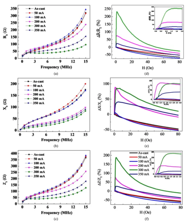
Figure 3a-c depict the zero-ield frequency dependence of the resistance R(H0), inductive reactance X(H0) and impedance
Z(H0) with different current amplitude of 0~350 mA. Obvious monotonic increasing trends in the resistance R(H0) (Figure 3a), inductive reactance X(H0) (Figure 3b), and impedance
Z(H0) (Figure 3c) are observed with the frequency range of 100 kHz ~ 15 MHz. The values of R and Z show the trends of irstly increasing less than 100 mA CJA compared with that of as-cast wires, then decreasing with the currents increase to minimum values at 300 mA CJA. Compared with R(H0) and Z(H0), the values of X(H0) with current amplitude larger than 200 mA are much smaller than those with corresponding values in current amplitude larger than 100 mA at high frequency (ƒ>1 MHz). It illustrates that the DS has changed a lot when the annealing current amplitude larger than 200 mA. Figure 3d-f display the ields dependence of the magneto-resistance ΔR/R (%) (d), magneto-inductive reactance ΔX/X (%) (e) and magneto-impedance ΔZ/Z (%) (f) ratios at ƒ=10 MHz for different annealing currents. The insets give the magniied plots of curves at the peak positions. After 200 mA CJA-ed microwire, the magneto-resistance ratio ΔR/R (%) and magneto-inductive reactance ΔX/X (%) reach to maximums of 76.4% and 88.9% at Hex=1.0 Oe, respectively. The magneto-impedance ΔZ/Z0 (%) is up to 76.9% at Hex=0.8 Oe. After 300 mA CJA, the ratio of (ΔR/R)max (%) is 232.7% at Hex=1.4 Oe, the (ΔX/X)max (%)
is 86% at Hex=3 Oe and the (ΔZ/Z0)max (%) is 188.1% at the
Hex=1.8 Oe. After 350 mA CJA, the (ΔR/R)max (%) decreases to 24.9% at Hex=1.4 Oe, the (ΔX/X)max (%) decreases to 40.9% at Hex=5 Oe and the (ΔZ/Z)max (%) decreases to 27.3% at
Hex=2 Oe due to the over Joule heated with large current. The maximum value of ΔX/X (%) obtained after 200 mA CJA. The reason for this behavior can be inferred for the anisotropy ield induced by the couple effect between the large radial stress for the large temperature gradient with the circumferential ield and the inner axial ield. These two factors play the main role for the physical properties of the microwires surface. The result of the coupling effect leads to the unique surface domain structure of the microwire. The phenomenon that the response of the ΔX/X (%) obviously hysteretic to the ΔZ/Z (%) nearly 1.2 Oe is resulting from the crystallization of inner part due to the over Joule heat under large current while the outer-shell part keeping amorphous microstructure owing to the protection of liquid nitrogen11. In this case, the induced circumferential ields observed for the ΔX/X (%) curves after 300 mA CJA appear a large platform without sharp peak which corresponding to the response ield Hex.
In fact, the impedance test is a dynamic magnetization process, during which the domain walls movement, magnetization rotation and the magnetic permeability µ changing alter the MI ratios. For the microwires with different preparation methods, the difference of domain structure
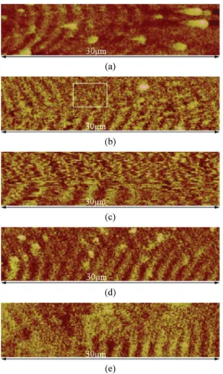
causes the disparity of response sensitivity to the external ield. In order to improve the circumferential permeability and change the magnetization process thus improving the MI effect, it is necessary to carry out annealing modulation for the microwire13. Figure 4 exhibits the microwires DSs
treated by different currents in CJA. For as-cast state, the weak circumferential domain with uneven width and indistinct wall due to the residual stress generated during preparation process is displayed in Figure 4a. The average width of weak circumferential domains is about 1.1 µm. The DS for 100 mA CJA-ed microwire is still an unclear circumferential domain with width of 0.9 µm. Most areas of the surface microwire are illed by unclear maze domains marked by white square zones. This DS almost exists in every CJA-ed microwire surface. After 200 mA CJA in Figure 4c, the width of local domain is about 1.71 µm with only a small part on the microwire surface. The majority of the surface domains are the maze domains. Notably, the circumferential domain is improved obviously for a large proportion of the microwire surface with clear domain wall and width of 0.94 µm for 300 mA CJA wire as seen in Figure 4d. This state corresponds to the large GMI ratio with relatively higher circumferential permeability µφ. For larger current of 350 mA CJA in Figure 4e, only a small proportion shows circumferential domain width is about 0.94 µm and most areas are the maze domains. In this case, the maze domain distribution may be resulted from the competitive
effect between the atoms severe thermal motion aroused by the large Joule heat and the forming of domain ordering distribution induced by the low temperature cooling around the microwire. The expansion of maze domain distribution represents the increasing of the leakage magnetic energy.
Based on the dynamic domain model14µ dc=µ0
2M s
2/dq,
the permeability µdc∝d-1 (d is the width of dynamic domain
and q is the pinning force coeficient), the growth of dynamic
domain width and the domain wall pinning both are bad to obtain high magnetic permeability and GMI effect. Therefore, it is very important to select a suitable parameter
Figure 3. Frequency dependence of (a) resistance R(H0), (b) inductive reactance X(H0) and (c) impedance Z(H0) and ield dependence of (d) magneto-resistance (ΔR/R0), (e) magneto-reactance (ΔX/X0), and (f) magneto-impedance (ΔZ/Z0) ratios with annealing current in the range of 0~350 mA. Insets of the magniied peak positions of ΔR/R0, ΔX/X0 and ΔZ/Z0 in (d), (e) and (f) respectively.
resulting in higher GMI ratio and response sensitivity (seen in Figure 4d). Combined with the large response ield range of 1.8 Oe, the microwire during the CJA can be considered as promising miniaturized and high sensitive GMI sensors.
4. Conclusion
In conclusion, we have conducted a systematic investigation of the effect of CJA on melt-extrated Co68.15 Fe4.35Si12.25B13.25Nb1Cu1 microwires. We obtained the direct evidence that the enhanced GMI effect under large current annealing result from the improving the circumferential domains through the surrounding nitrogen gap for cooling and coupling effect between the radial stress ield and induced circumferential ield, respectively. After 300 mA CJA, the maximum ΔZ/Z (%) achieves to 188.1% with ield
sensitivity ξ of 104.5 (%/Oe). Moreover, the linear response range expands to 1.8 Oe. Based on the cryogenic effect, large annealing current amplitude to 350 mA is achieved for the GMI proile. Therefore, an effective method to modulate the GMI effect towards a wider response ield range for sensor applications is obtained.
Acknowledgements
D.M.C. acknowledges the inancial support provided by the Natural Science Foundation of China (NSFC) under Grant No. 51371067. J.S. Liu acknowledges the inancial support provided by the National Natural Science Foundation of China (NSFC) under grant Nos. 51401111 and 51561026, Natural Science Foundation of Inner Mongolia Autonomous Region of China (NSFC) under grant Nos. 2014BS0503, and Scientific Research Foundation of the Higher Education Institutions (SRFHEI) of Inner Mongolia Autonomous Region of China (SRFHEI) under grant Nos. NJZY14062.
References
1. Phan MH and Peng HX. Giant magnetoimpedance materials: fundamentals and applications. Progress in Materials Science. 2008; 53(2):323-420. http://dx.doi.org/10.1016/j.pmatsci.2007.05.003.
2. Panina V, Mohri K, Bushida K and Noda M. Giant magnetoimpedance and magnetoinductive effects in amorphous alloys. Journal of Applied Physics. 1994; 76(10):6198-6203. http://dx.doi. org/10.1063/1.358310.
3. Vázquez M, Knobel M, Sanches R, Valenzuela A, and Zhukov AP. Giant magnetoimpedance effect in soft magnetic wires for sensor applications. Sensors and Actuators. A, Physical. 1997; 59(1-3):20-29. http://dx.doi.org/10.1016/S0924-4247(97)80143-4.
4. Pirota KR, Kraus L, Chiriac H and Knobel M. Magnetic properties and giant magnetoimpedance in a CoFeSiB glass-covered microwire. Journal of Magnetism and Magnetic Materials. 2000; 221(3):L243-L247. http://dx.doi.org/10.1016/ S0304-8853(00)00554-0.
5. Zhang SL, Sun JF, Xing DW, Qin FX and Peng HX. Large GMI effect in Co-rich amorphous wire by tensile stress. Journal of Magnetism and Magnetic Materials. 2011; 323(23):3018-3021. http://dx.doi.org/10.1016/j.jmmm.2011.06.041.
Figure 4. Magnetic domain structures of melt-extracted Co-based amorphous wires: (a) as-cast state; (b) 100 mA; (c) 200 mA; (d) 300 mA; (e) 350 mA; Ruler point is axial direction of microwire.
6. Ciureanu P, Khalil I, Melo LGC, Rudkowski P and Yelon A. Stress-induced asymmetric magneto-impedance in melt-extracted Co-rich amorphous wires. Journal of Magnetism and Magnetic Materials. 2002; 249(1-2):305-309. http://dx.doi.org/10.1016/ S0304-8853(02)00548-6.
7. Popov VV, Berzhansky VN, Gomonay HV and Qin FX. Stress-induced magnetic hysteresis in amorphous microwires probed by microwave giant magnetoimpedance measurements. Journal of Applied Physics. 2013; 113:17A326-17A326-3. http://dx.doi. org/10.1063/1.4798278.
8. Liu JS, Qin FX, Chen DM, Shen HX, Wang H, Xing DW, et al. Combined current-modulation annealing induced enhancement of giant magnetoimpedance effect of Co-rich amorphous microwires. Journal of Applied Physics. 2014; 115:17A326-17A326-3.
9. Wang H, Xing DW, Wang XD and Sun JF. Fabrication and Characterization of melt-extracted Co-based amorphous wires. Metallurgical and Materials Transactions. A, Physical Metallurgy and Materials Science. 2011; 42(4):1103-1108. http://dx.doi.org/10.1007/s11661-010-0459-0.
Materials. 2002; 242-245:224-228. http://dx.doi.org/10.1016/ S0304-8853(01)01254-9.
11 Chen DM, Xing DW, Qin FX, Liu JS, Shen HX, Peng HX, et al. Cryogenic Joule annealing induced large magnetic field response of Co-based microwires for giant magneto-impedance sensor applications. Journal of Applied Physics. 2014; 116:053907-053907-5. http://dx.doi.org/10.1063/1.4892042.
12. Liu JS, Cao FY, Xing DW, Zhang SL, Qin FX, Peng HX, et al. Enhancing GMI properties of melt-extracted Co-based amorphous wires by twin-zone Joule annealing. Journal of Alloys and
Compounds. 2012; 541:215-221. http://dx.doi.org/10.1016/j. jallcom.2012.05.126.
13. Chen DM, Xing DW, Qin FX, Liu JS, Wang H, Wang XD, et al. Correlation of magnetic domains, microstructure and GMI effect of Joule-annealed melt-extracted Co68.15Fe4.35Si12.2 5B13.75Nb1Cu0.5 microwires for double functional sensors.
Physica Status Solidi (a). 2013; 210:2515-2520. http://dx.doi. org/10.1002/pssa.201329246.