Brazilian Microwave and Optoelectronics Society-SBMO received 05 Oct 2017; for review 10 Oct 2017; accepted 21 Dec 2017
Brazilian Society of Electromagnetism-SBMag © 2018 SBMO/SBMag ISSN 2179-1074
Abstract— A compact, polarization insensitive, wide stop band frequency selective surface is presented. The unit cell is designed by modifying the basic square loop FSS. The simulated value of bandwidth for transmission < ‒ 20 dB for TE incident wave is 7.7 GHz from 4.71 GHz to 12.41 GHz which is 89.95% corresponding to the center frequency of this range. It has an excellent band stop response for C and X band. The periodicity of the unit cell is the order of 0.33λ0 at the center frequency of 8.56 GHz. The total
thickness of the proposed structure is 1.6mm (0.045λ0). Standard
design formulas are used to evaluate the resonance frequencies and calculated values are found to be very close to the simulated ones. The proposed design is polarization insensitive and has good angular stability. An array of the proposed design is fabricated on either side of dielectric substrate FR4. The measured and simulated transmission responses are in good agreement. Proposed design can be used for many potential applications such as electromagnetic shielding, spatial filtering, sub - reflector in antennas and RCS reduction etc.
Index Terms—Frequency selective surface, polarization insensitive, compact, wideband, band stop.
1INTRODUCTION
Electromagnetic band gap (EBG) structures [1], partially reflective surfaces (PRSs) [2], and artificial
magnetic conductors (AMCs) [3] are extensively investigated for their variety of applications in microwave
and millimeter wave regimes. A perfect design of the ground plane beneath the antenna attracts much of the
attention due the challenge of improving the various characteristics such as gain, bandwidth and directivity
etc. AMCs and PRSs such as Frequency Selective Surfaces (FSSs) [4-6] are used as the ground plane to
improve the aforementioned characteristics of the antenna. FSSs are also used as dichroic sub-reflectors in
dual frequency antennas, superstrate in antennas to increase directivity, for radar cross section reduction, as
polarizers and spatial filters. They are also used as a special reflector to maintain purity of signal transmitted
or received in satellite communication.
FSSs are usually designed to give frequency responses like band stop, band pass, high pass and low pass
spatial filter [7]. Their performance depends upon an element type, its shape, size, periodicity, polarization,
incident angle and thickness of the dielectric layer [8]. Conventional FSS shapes, such as loop type, center
connected and solid interiors are limited in their performance due to narrow transmission bandwidth for
Polarization Insensitive Compact Wide
Stop-band Frequency Selective Surface
D. Sood*, C. C. Tripathi,
Department of Electronics & Communication Engineering, University Institute of Engineering & Technology, Kurukshetra University, Kurukshetra
Brazilian Microwave and Optoelectronics Society-SBMO received 05 Oct 2017; for review 10 Oct 2017; accepted 21 Dec 2017
Brazilian Society of Electromagnetism-SBMag © 2018 SBMO/SBMag ISSN 2179-1074 incident waves. Use of multiple FSS layers to achieve wide transmission response is a common approach
[9-11]. This makes the structure unsuitable for planar applications due to increase in its overall thickness.
However, loop type FSSs are highly investigated due their wideband response. Square Loop type FSSs have
been analyzed and synthesized using several techniques [12-14]. A wide stop-band cascaded frequency
selective surface by using koch fractal elements is proposed in [15]. In this, wide stop band is achieved by
cascading two FSS screens of 1.27mm thick each, with an air gap of 2mm, which increases its overall
thickness. Similarly, a wide stop band FSS is presented in [16]. It is a single layer design, but the substrate
used is of large thickness (3.2 mm), which limits its use for planar applications. A thin, compact, symmetric
and ultra-wide stop band FSS is proposed in [17] but it covers only 3.5 GHz of (-20db transmission)
bandwidth in ultra-wide band range. Another wide stop band FSS design has been proposed in [18].
However, it is polarization insensitive but its substrate thickness is large and its -20dB transmission
bandwidth is almost nil. A compact, ultra wide band square loop FSS has also been proposed in [18]. It
covers 8 GHz of -20db transmission bandwidth, but it lacks in rotational symmetry which makes it sensitive
to incident wave polarization and its center frequency varies w.r.t different incident angles.
In this paper, a compact and polarization insensitive FSS, with a wide stop band characteristics has been
designed. Periodicity of the unit element is nearly 0.33λ0. The design has rotational symmetry which helps to achieve polarization insensitivity. Thickness of the proposed FSS is 0.045λ0 at center frequency of 8.56GHz,
which is much smaller than the conventional multilayer FSS. Proposed FSS can be used for bandwidth
enhancement of antennas, as reflecting surface and microwave shield for C and X bands. All analysis has
been carried out using the Ansoft’s HFSS v.14. A prototype of the proposed FSS is fabricated on both sides
of dielectric FR4 (εr = 4.4).
The presented paper is organized as follows: Section II describes the theory of operation and FSS design.
Section III outlines the simulation results with parametric analysis of the FSS and in section IV experimental
verifications are outlined with a comparison with simulation results. In section V the work is summarized in
a brief conclusion.
2DESIGN &SIMULATION
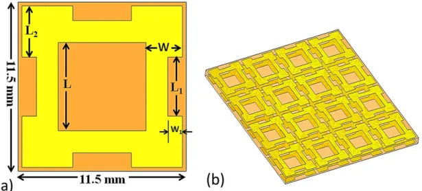
The unit cell of the proposed FSS is shown in Fig. 1(a). Initially, a single square loop FSS has been formed and then we modify the design proposed in [18] and made a rotational symmetric structure to achieve
polarization insensitivity. It consists of top and bottom metallic layers of a 2-D periodic array, of modified
square loop patches as illustrated in Fig. 1(b). The overall size of the single unit cell is 11.5mm × 11.5mm,
which is equal to 0.33λ0. The optimized dimensions are L = 6mm, L1 = 4mm, L2 = 3.5mm, W = 2.5 mm and W1 = 1 mm. The overall thickness of structure is 1.6 mm. For achieving compactness, the conventional
square loop type FSS structure is modified by cutting the slots of the size W1 × L1 symmetrically. The slot
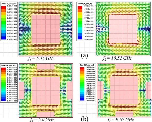
cutting increases the current path. The surface current distributions of the conventional and proposed FSSs
Brazilian Microwave and Optoelectronics Society-SBMO received 05 Oct 2017; for review 10 Oct 2017; accepted 21 Dec 2017
Brazilian Society of Electromagnetism-SBMag © 2018 SBMO/SBMag ISSN 2179-1074
the cutting of slots results meandering in the path as compared to a normal conventional square loop
and the currents has travel longer paths. Due to this increase in current path
the proposed FSS exhibitslower resonance frequency in comparison to the conventional square loop as shown in Fig. 3(a). Proposed
FSS provides two transmission nulls ‘f1’ and ‘f2’ of 5.0 and 9.67 GHz respectively with -20dB transmission
bandwidth of 7.7 GHz. The simulated phase response has also been investigated as represented in Fig. 3(b). The phase changes linearly over the wide stop band exhibited by the proposed FSS. This linearly decreasing
phase makes it useful for its potential application in pulsed systems [19].
Brazilian Microwave and Optoelectronics Society-SBMO received 05 Oct 2017; for review 10 Oct 2017; accepted 21 Dec 2017
Brazilian Society of Electromagnetism-SBMag © 2018 SBMO/SBMag ISSN 2179-1074 Fig. 2. Surface current distribution of (a) conventional square loop FSS and (b) the proposed FSS structures for their transmission
null frequencies.
Fig. 3. (a) Comparison of simulated S21 of the proposed FSS with conventional square loop FSS and (b) simulated phase response.
The simulated polarization response of the proposed FSS is shown in Fig. 4(a). As the polarization angle varies the electric field (E) and magnetic field (H) makes an angle ‘ϕ’ with the X-axis and Y-axis,
respectively, but the direction of propagation is maintained along Z-axis. The proposed structure exhibits
polarization insensitivity as for the variations of angle ‘ϕ’ from 00 to 900 the transmission response remains
same and both the resonant frequencies remains constant. The performance of the proposed FSS has also
Brazilian Microwave and Optoelectronics Society-SBMO received 05 Oct 2017; for review 10 Oct 2017; accepted 21 Dec 2017
Brazilian Society of Electromagnetism-SBMag © 2018 SBMO/SBMag ISSN 2179-1074 varying angles of incident wave from 00 to 600. Therefore, the overall bandwidth almost remains unaffected
with the change in angles and the structure shows good performance for high incident angles such as 600.
Fig. 4. Simulated response (a) for different polarization angles and (b) for different oblique incidence angles
As the bandwidth of the loop type FSS is mainly dependent upon its width and the cutting of slots, reduces
the width (W) of the proposed square loop which further decreases the bandwidth. To solve this problem, the
dimensions of W1 and L1 are critically optimized to maintain the effective width nearly constant.
3EQUIVALENT CIRCUIT ANALYSIS
The equivalent circuit method is used to understand the basic theory of operation of the proposed design.
Equivalent circuit is shown in Fig. 5. The Impedance of the dielectric material is calculated as 𝑍𝐷= 𝑍0/√𝜀𝑟 (Z0 is free space impedance i.e. 377Ω). Loop type FSS patch is modeled by the parallel combination of LF
and CF. From the simplified equivalent circuit of square loop FSS suggested in [20] the values of inductance
(LD) and capacitance (CD) of dielectric substrate as well as of the conventional square loop are calculated
using the following equations:
L
D= µ
0µ
rh
(1)
C
D= (ε
0ε
rh)/2
(2)
XLFZ0
=
d
p
F
1(p, W, λ)
(3)
BCFY0
= 4
d
p
F
2(p, g, λ)
(4)
F
1(p, W, λ) =
pλ[ln (cosec
πW2p) + G
1(p, W, λ)]
(5)
Brazilian Microwave and Optoelectronics Society-SBMO received 05 Oct 2017; for review 10 Oct 2017; accepted 21 Dec 2017
Brazilian Society of Electromagnetism-SBMag © 2018 SBMO/SBMag ISSN 2179-1074 Fig. 5. Equivalent circuit of the proposed FSS.
Where µ0 is the permeability of the free space, µr is the relative permeability of dielectric substrate, ‘h’ is the height of the dielectric substrate, ε0 is the permittivity of free space, εr is the relative permittivity of the dielectric, ‘p’ is the periodicity, ‘W’ is the width of the loop, ‘g’ is the gap between two unit elements and
‘d’ is the dimension of square loop. G1(p, W, λ) and G2(p, g, λ) are correction factors. From the equations, (1) to (6) the values of the lumped parameters are calculated and given in Table I.
TABLE I CALCULATED VALUES OF LUMPED PARAMETERS.
S. No. Parameter Calculated Value
1 LD 2.011nH
2 CD 0.031pF
3 L 2.610nH
4 C 0.130pF
The simulated value of first resonance frequency (f1) is 5.0 GHz. The first and second resonance frequencies
are calculated by using methods as suggested in [18]. The first resonance frequency (f1) is calculated as:
𝑓
1=
12𝜋√(𝐿𝐷+𝐿𝐹2)(𝐶𝐷+2𝐶𝐹)
(7)
LD and CD are the inductance and capacitance of the dielectric substrate respectively. The calculated value of
first resonance frequency ‘f1’ is 5.12 GHz which is very close to the simulated value. The second resonance
frequency ‘f2’ of the proposed FSS design depends upon ‘W’, ‘L1’ and ‘W1’. The second resonance frequency has been evaluated by formulation of an equation through the use of curve fitting as:
𝑓
2= a(e
bW)
(8)
Brazilian Microwave and Optoelectronics Society-SBMO received 05 Oct 2017; for review 10 Oct 2017; accepted 21 Dec 2017
Brazilian Society of Electromagnetism-SBMag © 2018 SBMO/SBMag ISSN 2179-1074
𝑎 = 2.1233 − 0.3291𝑊
1(9)
𝑏 = 0.6469 + 0.0059𝐿
1(10)
The values of ‘W’, ‘W1’ and ‘L1’ are in mm. The simulated and calculated values are compared as listed in
Table II, Table III and Table IV. It is observed that for the optimized dimensions of W, W1 and L1 the
percentage errors in between the simulated and calculated values are quite less which shows the good
convergence of the
fitted equation
.TABLE II COMPARISON OF DIFFERENT VALUES OF W (L1 =4 mm, W1 =1 mm).
S. No. W (mm) Simulated f2
Calculated f2
%Error
1 2.00 7.08 6.89 2.68
2 2.25 8.09 8.11 0.25
3 2.50 9.67 9.59 0.83
4 2.75 11.56 11.34 1.90
TABLE III COMPARISON OF DIFFERENT VALUES OF W1 (L1 = 4 mm, W =2.5 mm).
S. No. W1 (mm) Simulated f2
Calculated f2
%Error
1 0.5 9.98 10.47 4.90
2 1.0 9.67 9.59 0.93
3 1.5 9.25 8.71 5.83
4 2.0 8.30 7.84 5.54
TABLE IV COMPARISON OF DIFFERENT VALUES OF L1 (W1 = 1 mm, W =2.5mm).
S. No. L1 (mm) Simulated f2
Calculated f2
%Error
1 2 9.25 9.31 0.64
2 3 9.33 9.45 1.28
3 4 9.67 9.59 0.83
4 5 9.83 9.73 1.01
4PARAMETRIC ANALYSIS
In order to get better physical insight and to investigate the contribution of different geometric dimensions in
wideband response the parametric analysis of the proposed FSS has been done. The simulated transmission
response for different value of ‘W’ is shown in Fig. 6(a). It is observed that as the width (W) increases second resonant frequency greatly affected and shifts towards higher value thereby enhances the bandwidth.
The maximum bandwidth achieved is 9.32 GHz for ‘W’ equals to 2.75 mm from 4.79 to 14.11 GHz, which
is 98.62% corresponding to the center frequency of this range. However, the increase in width (W) above
2.50 mm (optimized value) results increase in bandwidth, but it shifts the second resonant frequency to a
higher value which further disturbs the compactness of the proposed design. Transmission response for
different values of the slot width (W1) is shown in Fig. 6(b). It is observed that as the slot width increases second resonant frequency shifts towards lower value due to increase in effective inductance and causes the
decrease in -20dB bandwidth. The optimized value of W1 is 1 mm. The effect of slot length (L1) on the
Brazilian Microwave and Optoelectronics Society-SBMO received 05 Oct 2017; for review 10 Oct 2017; accepted 21 Dec 2017
Brazilian Society of Electromagnetism-SBMag © 2018 SBMO/SBMag ISSN 2179-1074 variation in first resonance frequency but the second resonance frequency increases slightly which further
increases the bandwidth and the optimized value of L1 is found to be 4 mm.
Fig. 6. Simulated response of the proposed FSS (a) for different values of width ‘W’ (b) for different values of width ‘W1’ and (c) for
different values of width ‘L1’
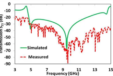
5EXPERIMENTAL VERIFICATIONS
In order to experimentally measure the performance of the proposed wideband FSS structure an array of 17 ×
17 elements has been fabricated as shown in Fig. 7(a). For the measurements of transmission response (S21) two double ridge ultra-wide band horn antennas (1 to 18GHz), connected to Agilent’s Vector Network
Analyzer (VNA) model N5222A are used. One of the horn antennas is used as a transmitter and the other as
a receiver. At first, in order to calibrate the test setup S21 is measured by placing the two antennas in front of
each other at a distance of nearly 1.2 meters. Then measurement of S21 was performed by placing fabricated
prototype of FSS in between the two horn antennas as shown in Fig. 7(b). The difference between the two measured results gives rise to actual transmission response of the fabricated FSS structure. The measured
Brazilian Microwave and Optoelectronics Society-SBMO received 05 Oct 2017; for review 10 Oct 2017; accepted 21 Dec 2017
Brazilian Society of Electromagnetism-SBMag © 2018 SBMO/SBMag ISSN 2179-1074 Fig. 7. (a) Fabricated prototype of the proposed FSS and (b) measurement setup.
Fig. 8. Comparison of measured and simulated transmission response (S21) under normal incidence.
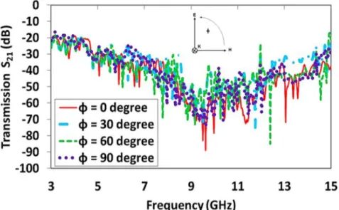
The polarization insensitivity of the fabricated design is tested by measuring its transmission response for
different azimuthal angles (ϕ) as shown in Fig. 9. In order to measure polarization response, the fabricated structure is rotated about its axis from 00 to 900 in the steps of 300. It is observed that similar to simulated
response the measured transmission response remains same for all polarization angles (ϕ), which proves
polarization insensitivity of the proposed FSS structure. Fabricated prototype is also tested experimentally
for oblique incidences by rotating transmitting antenna around the circumference of a circle whose radius is
equal to the distance at which near field effects are observed to be minimum. The experimental results for
Brazilian Microwave and Optoelectronics Society-SBMO received 05 Oct 2017; for review 10 Oct 2017; accepted 21 Dec 2017
Brazilian Society of Electromagnetism-SBMag © 2018 SBMO/SBMag ISSN 2179-1074 Fig. 9. Measured transmission response (S21) for different polarization angles under normal incidence.
Fig. 10. Measured transmission response (S21) for different incident angles under TE polarization.
6CONCLUSIONS
A compact, polarization insensitive, wide stop band frequency selective surface has been presented. The
unit cell of the proposed design consists of a modified square loop FSS printed on either side of FR4
substrate. Overall thickness and periodicity of the design is 1.6mm (0.045λ0) and 11.5 mm (0.33 λ0) respectively. The proposed FSS has wide stop band (transmission response < ‒ 20dB) of 7.7 GHz, which
covers both C and X band. Equivalent circuit of the proposed design is presented and resonance frequencies
are calculated to validate their values in comparison to simulated ones. The performance of the proposed
FSS design is investigated for its various dimensional parameters to find best optimal solution. The
Brazilian Microwave and Optoelectronics Society-SBMO received 05 Oct 2017; for review 10 Oct 2017; accepted 21 Dec 2017
Brazilian Society of Electromagnetism-SBMag © 2018 SBMO/SBMag ISSN 2179-1074 Measured results are observed in agreement with the simulated results. The unit cell size, thickness and other
features of the proposed FSS have been compared with the previously reported wide stop-band FSS designs
in Table V. It is observed that the proposed FSS is compact and provides large percentage bandwidth as
compared to [15, 16]. However, the designs presented in [18] and [21] exhibits more percentage bandwidth
but the proposed design is polarization insensitive as compared to [18] and is more compact in size as
compared to [21]. These features make it suitable for various potential applications such as RCS reduction,
pulsed systems, electromagnetic shielding, spatial filtering, sub -reflector in antennas etc.
TABLE V COMPARISON OF THE PROPOSED FSS WITH PREVIOUSLY PRESENTED DESIGNS.
FSSs Center Frequency
(GHz)
Unit Cell Size (mm)
Thickness (mm)
-20 dB Stop band Bandwidth (GHz) Metallic Layers used Polarization Insensitive
[15] ~8.5 9.0
(0.30 λ0)
3.27
(0.92 λ0)
~5.0 (~60%)
Multilayer Yes
[16] 10.25 12.0
(0.041 λ0)
3.20
0.11 λ0)
7.50 (73.17%)
Dual Layer Yes
[18] 6.87 16.0
(0.37 λ0)
1.80
(0.041 λ0)
8.0 (116%)
Dual Layer No
[21] 7.63 14.0
(0.36 λ0)
1.60
(0.041 λ0)
7.53 (98.62%)
Dual Layer Yes
Proposed FSS
8.56 11.5
(0.33 λ0)
1.60
(0.045 λ0)
7.70 (89.95%)
Dual Layer Yes
ACKNOWLEDGMENT
This work was financially supported by word bank assisted project TEQIP-II (subcomponent 1.1) under
section 12B & 2f for graduate studies. The authors want to thank Dr. Saptarshi Ghosh and Dr. Somak
Bhattacharrya (Ex PhD Scholars), Department of Electrical Engineering, IIT, Kanpur, India for their
valuable suggestions for the completion of this work specially measurements and testing.
REFERENCES
[1] E. Yablonovitch, “Photonic bandgap structures,”J Opt. Soc. (America B), vol.10, pp. 283–295,1993. [2] G. V. Trentini, “Partially reflecting sheet arrays,”IRE Trans. Antennas Propaga.,” vol. 4, pp. 666 – 671, 1956.
[3] Y. Zhang, J. Von Hagen, M. Younis, C. Fischer, and W. Wiesbeck, “Planar artificial magnetic conductors and patch antennas,” IEEE Trans. Antennas Propaga., vol. 51, pp. 2704 -2712, 2003.
[4] D. J. Kern, D. H. Werner, A. Monorchio, L. Lanuzza, M. J. Wilhelm, “The design synthesis of multiband artificial magnetic conductors using high impedance frequency selective surfaces,”IEEE Trans. Antennas Propag., vol. 53, pp. 8-17,2005. [5] A. Monorchio, G. Manar,a, L. Lanuzza, “Synthesis of artificial magnetic conductors by using multilayered frequency selective
surfaces,”IEEE Antennas Wireless Propag. Lett., vol.1, pp.196-199, 2002.
[6] M. A. Hiranandani, A.B. Yakovlev, and A.A. Kishk, “Artificial magnetic conductors realised by frequency-selective surfaces on a grounded dielectric slab for antenna applications,”IEE Proc. Microw. Antennas Propag., vol.153, pp. 487-493, 2006.
[7]B. A. Munk, Frequency selective surfaces: Theory and design, Wiley, New York, 2000.
[8] R. Mittra, C.H.Chan, and T. Cwik, “Techniques for analyzing frequency selective surfaces-A review,”IEEE Proc., vol.76, pp. 1593-1615, 1998.
[9] F. C. G. d’ Segundo, Antonio L. P. S. Campos, A. G. Neto, “A design proposal for ultrawide band frequency selective surface,”J Microw. Optoelectron. Electromagn. Appl.,” vol.12, pp. 398-409, 2013.
[10] L. Moustafa, B. Jecko, “Design and realization of a wide-band EBG antenna based on FSS and operating in the Ku-band,”Int. J Antennas Propag, vol. 139069, pp.1-8, 2010.
Brazilian Microwave and Optoelectronics Society-SBMO received 05 Oct 2017; for review 10 Oct 2017; accepted 21 Dec 2017
Brazilian Society of Electromagnetism-SBMag © 2018 SBMO/SBMag ISSN 2179-1074 [12] X. F. Luo, P.T. Teo, A. Qing, C.K. Lee, “Design of double square loop frequency selective surfaces using differential evolution
strategy coupled with equivalent circuit model,”Microwave Opt. Technol. Lett., vol. 44, pp.159-162, 2005.
[13] A.L.P.S. Campos, A.M. Martin, V.A. Almeida Filho, “Synthesis of frequency selective surfaces using genetic algorithm combined with the equivalent circuit method,”Microwave Opt. Technol. Lett., vol.54, pp. 1893-1897, 2012.
[14] K. R. Jha, G.Singh and R. Joyti, “A simple synthesis technique of single square loop frequency selective surface,”Progress In Electromagnetics ResearchB, vol. 45, pp.165-185, 2012.
[15] R. H. C. Maniçoba, A. G. d’Assunção, A. L. P. S. Campos, “Wide stop-band cascaded frequency selective surfaces with koch fractal elements,”Proc. 14th Biennial IEEE Conference on Electromagnetic Field Computation (CEFC), Chicago(USA), pp. 1, May, 2010.
[16] I. S. Syed, Y. Ranga, L. Matekovits, K. P. Esselle, and S. G. Hay, A single-layer frequency-selective surface for ultrawideband electromagnetic shielding, IEEE Trans Electromagn Compat 56 (2014),1404-1411.
[17] S. Baisakhiya, R. Sivasamy, M. Kanagasabai, S. Periaswamy, “Novel comapct UWB frequency selective surface for angular and polarization independent operation,”Progress In Electromagnetics Research Lett., vol. 40, pp.71-79, 2013.
[18] N. Kushwaha, R. Kumar, R.V.S. R. Krishna and Tuhina Oli, “Design and analysis of new compact UWB frequency selective surface and its equivalent circuit,”Progress In Electromagnetics Research C, vol. 46, pp. 31-39, 2014.
[19] F.C.G. da Silva Seundo, A.L.P. de Siqueria Campos, “A design proposal for ultrawide band Frequency Selective Surface”, J Microw. Opto. Electromagn. Appl., vol. 12, pp.398-409, 2013.
[20] R. J. Langley and E.A. Parker, “Equivalent circuit model for arrays of square loops,”Electron Lett., vol.18, pp. 294-296, 1982. [21] R. Sivasamy, B. Moorthy, M. Kanagasabai, J. V. George, L. Lawrance, D. B. Rajendran, “Polarization-independent single-layer