DOI: 10.13164/re.2015.0455 ELECTROMAGNETICS
Gain Enhancement of a Wide Slot Antenna Using
a Second-Order Bandpass Frequency Selective Surface
Ayan CHATTERJEE, Susanta Kumar PARUI
Dept. of Electronics & Tele-Comm. Engineering, Indian Institute of Engineering Science & Technology, Shibpur, Howrah-711103, India
[email protected], [email protected]
Abstract. Gain enhancement of a wide slot antenna over a wide frequency band using a low profile, second order bandpass frequency selective surface (FSS) as a super-strate is presented in this paper. The proposed multilayered FSS with non-resonant unit cells in each layer allows in-phase transmission of waves radiated from the antenna over a 3dB bandwidth of about 50%. The design allows an enhancement of up to 4 dBi in the antenna gain over the entire frequency band (5-8 GHz) of operation. The FSS provides a very low insertion loss between the two trans-mission poles along with a linearly decreasing transmis-sion phase over the band. The composite structure shows an impedance bandwidth (-10 dB) of 65% with an average gain between 6-8 dBi over the frequency band with a peak gain of 9 dBi. Measurement results of the fabricated pro-totype matches well with the predicted values.
Keywords
Wide slot, Frequency Selective Surface, gain, bandpass, superstrate.
1.
Introduction
With the increasing demand of high data transmission rates, short pulse transmission and easy integration with the feed networks or MMICs, wide band and ultra-wide band (UWB) slot antennas are being widely used in the commu-nication systems and have become a great interest of re-searchers. These antennas find applications in ground pen-etrating radar (GPR), medical imaging, multimedia com-munications, etc. [1]. Till date several methods have been proposed for widening the bandwidth of slot antennas [2], [3]. In general, these antennas radiate in both directions orthogonal to the radiating plane whereas applications involving line-of-sight (LOS) communication and high signal to noise ratio (SNR) require a directional or semi-omnidirectional (wide-beam) radiation patterns. Directional radiation from the antenna also provides enhanced gain in the broadside direction along with reduced side lobe levels (SLL) [4] finding its application in the radar and millimeter wave systems. Enhancement of gain or directivity of these
antennas in a specific direction over a wide band of fre-quencies is a challenging job and very few movements have been made so far in this regard. A broadside series-fed printed antenna array with a large slot in the ground plane was introduced [4] leading to enhancement in the gain by about 2-3 dB over the whole frequency band but a reasonable increase in the antenna size was required due to the array structure.
Recently, Frequency Selective Surfaces (FSS) are being used in the form of substrates or superstrates [5–11] for the enhancement of antenna performances. Metal type FSS superstrates are much easier to fabricate than the die-lectric type. Alireza Foroozesh et al. presented a cavity resonance antenna (CRA) [6], where a patch type FSS has been used as superstrate at a distance of around half wave-length with respect to center frequency from the antenna and both gain and directivity have been efficiently enhanced over the impedance bandwidth. Abbas Pirhadi et al. have investigated an electromagnetic bandgap (EBG) antenna [7] where a FSS with square loop elements was used as superstrate above the microstrip patch, leading to enhanced directivity and wide bandwidth. A technique for achieving highest possible gain for a patch antenna at the resonating frequency was proposed [8] where a magnetic material (relative permeability 50) was used as superstrate with less than conventional half wavelength spacing. The use of FSS superstrates for dual-band directivity enhance-ment was introduced by Lee et al. [9] that comprise two FSS screens with about half wavelength spacing between them at a height of about half wavelength from the antenna which makes the overall height almost one wavelength and it is to be reduced for low profile applications.
2.
Antenna-FSS Configuration
The proposed structure is composed of a wide slot antenna and a FSS superstrate as shown in Fig. 1 and Fig. 2 showing its side view and three dimensional views.
2.1
Design of the Wide Slot Antenna
A simple design of a microstrip line fed slot antenna
was proposed by Jen-Yea Jan et al. [12] where a square
shaped slot was chosen in the ground plane with a specific angle of rotation to excite two close resonant frequencies leading to a wide bandwidth. Following this procedure,
a slot antenna is designed in the frequency band of
5-8 GHz for the purpose of gain enhancement over the entire operating band. Length of the slot determines the first resonating frequency and these slots radiate like a half wave dipole whose length is half of the wavelength corre-sponding to the resonating frequency. So for exciting the first resonance near 5.7 GHz, size of the slot has been cho-sen half of the guided wavelength corresponding to 5.7 GHz and is given in the following equation:
(
)
0
Slot length=
2 r r 1 / 2
C
f ε +
(1)
where C0 is the speed of light in free space (3×10⁸ m/s),
fr is the desired resonating frequency (5.7 GHz) and εr
Fig. 1. Geometry of the FSS-antenna composite structure
(side view).
Fig. 2. Three dimensional view of the slot antenna with FSS
(all dimensions are in mm).
(εr = 4.4 for FR4) is the relative permittivity of the
sub-strate. The substrate thickness is hS = 1.6 mm. The above
equation gives a slot length of 16 mm. To achieve the sec-ond resonance near 7.5 GHz, the slot has been rotated at an angle of 45° about y axis and for optimal matching, length of the microstrip feed line has been chosen to be 18.5 mm.
2.2
Design Principle of the FSS Layers
A low profile FSS structure offering second order band pass filtering property, has been used as a superstrate layer above the antenna for the purpose of gain enhance-ment. The second order band pass response has been achieved by cascading three FSS layers of
patch-aperture-patch type with FR4 as the dielectric material (εr= 4.4) in
between them as shown in Fig. 2. Unit cells of the patch and aperture type layers exhibiting capacitive and inductive properties respectively are also shown in the figure. They do so due to their non-resonant nature, where dimensions of the unit cells are much smaller than the wavelength corresponding to resonating frequency. Fig. 2 shows top
view of each layer, where PX and PY are horizontal and
vertical periodicities of the unit cells same for both types of
FSS screens and (P-s) is dimension of the patch in
capaci-tive layer (s being the spacing between individual patches
and PX= PY= P). Inductive wire grids in the middle layer
have a grid width of w. With the fact that periodicities of
the unit cells in each layer are same in X and Y directions,
the FSS structure is polarization independent with respect to the plane wave incident on it.
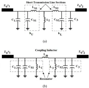
A simple equivalent circuit of the FSS is given in Fig. 3(a), valid for normal incidence of the electromagnetic wave. Being non-resonant in nature, the first and third
patch type layers are modeled as parallel capacitors C1 and
C3, whereas the middle aperture type grid layer is modeled
as a parallel inductor L2. Dielectric substrates separating
the metallic FSS layers of height hU and hL can be modeled
(a)
(b)
Fig. 3. (a) Simple equivalent circuit model of the cascaded
FSS. (b) Second order coupled resonator filter with π network (L1, Lm and L3) representation of T network
as two short pieces of transmission lines of characteristic impedances Z0/√εr1 and Z0/√εr2 respectively, where εr1 and
εr2 are dielectric constants of the substrates and Z0 = 377 Ω
is the free space impedance. The transmission line sections are represented here by their equivalent circuit model with a series inductor and a shunt capacitor. Half spaces on both ends of the cascaded FSS are modeled here as semi-infinite
transmission lines with characteristic impedances of Z0r1
and Z0r2 respectively (r1=r2= normalized source and load
impedances = 1). Second order nature of the filter is clearly visible in the circuit as shown in Fig. 3(b) where T network (consisting of LS1, L2 and LS2) of the circuit in Fig. 3(a) is
converted into a π network (consisting of L1, Lm and L3).
The values of L1, Lm and L3 can be easily found with the
values of LS1, L2 and LS2.
For the second order coupled resonator filter of Butterworth type response chosen, different parameters can be obtained from [14] and are given in Tab. 1.
Filter Type Normalized loaded quality factors Normalized coupling coefficient Normalized impedances
q1 q2 k12 Source (r1) Load (r2)
Butterworth 1.4142 1.4142 0.70711 1 1
Tab. 1. Different parameters for Butterworth filter response.
From the desired values of center frequency f0 and
fractional bandwidth (= BW/f0 corresponding to 3 dB
transmission bandwidth) along with the parameters
pro-vided in Tab. 1, the value of inductor L2 in the circuit of
Fig. 3(a) can be found by the following equation [13]:
(
)
(
)
2 12
0 1 2
2 2
0 12 12 1 2
.
(2 ) 1
k
Z r r
L
f k k q q
δ
π δ
= ⋅ ⋅
−
(2)
Using Telegrapher’s model for TEM transmission
lines, the inductors LS1 and LS2 representing the short
transmission line sections of the circuit in Fig. 3(a) can be calculated from the following equations:
1 0 1
S r U
L =µ µ h , (3)
2 0 2
S r L
L =µ µ h . (4)
The values of capacitors C1 and C3 representing the
capacitive (patch) layers of FSS can also be obtained from the following equations [13]:
(
)
1 0 1
1
0 0 1
,
2 2
r U
q h
C
f Z r
ε ε
π δ
= − (5)
(
)
2 0 2
3
0 0 2
.
2 2
r L
q h
C
f Z r
ε ε
π δ
= − (6)
The second terms in the above equations represent the
capacitors CS1 and CS2 of the short transmission line
sec-tions of the circuit in Fig. 3(a). For the proposed design, FR4 (glass-epoxy) has been chosen as the substrate mate-rial, for which εr1 = εr2 = εr = 4.4 and µr1 = µr2 = µr = 1 (the
dielectric substrate being non-magnetic).
The above equations along with the substrate
param-eters are now used to determine the inductor (L2) and
ca-pacitor (C1, C3) values of the Butterworth filter for desired
response of FSS with center frequency f0 = 6.5 GHz (of the
frequency band 5-8 GHz) and fractional bandwidth
= 0.46 (BW = 3 GHz). For available substrate thickness
hU = hL = 0.8 mm, the computed values are C1 = C3 =
184.4 fF and L2 = 1.1 nH. In the next step, dimensions of
the unit cells of both the capacitive and inductive layers of the FSS are determined by the following equations [13].
1
1 3 0 eff
2
ln sin 2
P s
C C C
P π ε ε π − = = =
, (7)
1
2 0 eff ln sin
2 2 P w L L P π µ µ π − = =
. (8)
From (7), with C = 184.4 fF, s = 0.3 mm, ε0 (free
space permittivity) = 8.85×10⁻¹² F/m and εeff (effective per-mittivity of the medium in which the patches are located) = (εr + 1)/2 = 2.7, the unit cell dimension P is first
ob-tained. The spacing between consecutive patches (s) is
selected so to avoid fabrication errors, at the same time allowing good angular stability [15]. Then with the value of
P, L = 1.1 nH, µ0 (free space permeability) = 4π × 10-7 H/m
and µeff (effective permeability of the medium in which the
inductive grids are located) = (µr + 1)/2 = 1, width of the
inductive wire grids is determined.
With the initially available dimensions of unit cells of the FSS layers, after a few successive full wave EM simu-lations, optimal dimensions are obtained and are given in Tab. 2 along with the values obtained from circuit model for the desired second order bandpass response. For EM simulations, HFSS is used.
Parameter PX = PY =P w s hU = hL
Circuit model 5.1 mm 1.1 mm 0.3 mm 0.8 mm Optimized 7 mm 1.6 mm 0.3 mm 0.8 mm
Tab. 2. Calculated and optimal dimensions of FSS unit cells.
2.3
Principle of Operation
Principle of operation of the composite structure can be well understood with the help of Fig. 1 and Fig. 4. The process of gain enhancement of the wide slot antenna can be justified with the phase vs. frequency characteristics of FSS and the composite structure. As discussed previously, the FSS is designed to exhibit bandpass characteristics in the frequency range of 5-8 GHz and as can be seen from
the transmission phase (φT as shown in Fig. 1) response of
the cascaded FSS structure in Fig. 4(b), the phase decreases linearly with frequency within the desired frequency band.
As can be observed from Fig. 1, waves radiated by the slot suffer a small amount of reflection from the lower metallic (patch) layer of the FSS and again get reflected by the ground plane, and phase delay of this round trip
propa-gation (φR as shown in Fig. 1) increases linearly with
2 2
R
f H c
π
ϕ = . (9)
The variation of φR with frequency is controlled by
the spacing H between antenna and FSS to produce a
co-herent wave from the composite structure with a zero phase
variation (total phase φ= φT + φR). The waves from the
structure thus go through a constructive interference of its components leading to an enhancement in gain over the entire frequency band.
3.
Characteristics of the Antenna with
FSS Superstrate
In the analysis of the proposed design, first antenna and FSS layers are investigated separately followed by the composite structure. Both simulation and measurement results are presented.
3.1
Characteristics of the FSS Layers
To analyze with HFSS, unit cells of the three FSS layers are placed inside a waveguide with master-slave boundaries on the four sides with a floquet port excitation given. Transmission and reflection coefficients of the structure are then obtained using full wave EM simulation and are shown in Fig. 4(a) with the transmission phase (degree) variation with frequency in Fig. 4(b).
As can be observed from Fig. 4(a), the FSS exhibits a pass band over 5-8 GHz with transmission level above
3 4 5 6 7 8 9 10
-25 -20 -15 -10 -5 0
Tr
ansm
is
si
on /
R
ef
lec
ti
on C
o
ef
fi
ci
en
t (dB)
Frequency (GHz)
Transmission Reflection
(a)
3 4 5 6 7 8 9 10
-200 -150 -100 -50 0 50 100 150 200
Trans
m
is
si
on
Pha
se
(D
eg)
Frequency (GHz)
(b)
Fig. 4. (a) Simulated transmission and reflection coefficient of
the FSS, (b) EM simulation of transmission phase of the FSS structure.
–3 dB with two transmission poles. From the phase vs. frequency plot, it is clear that, the phase is zero at both the transmission poles and has nearly linear variation with frequency in between. The FSS in its pass band gives an insertion loss of less than 1 dB at both the transmission poles and about 2.8 dB near the center frequency 6.5 GHz. Higher loss tangent (0.02) of FR4 in comparison to con-ventional microwave substrates accounts for this insertion loss. The 3 dB transmission as well as reflection bandwidth of the bandpass FSS is around 50% with respect to the center frequency.
3.2
Characteristics of the Antenna with FSS
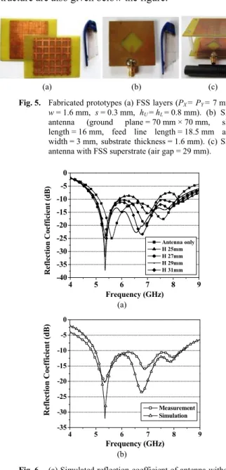
Fabricated prototypes of the FSS layers (patch and aperture type) and slot antenna along with the composite structure are shown in Fig. 5. Dimensions of the fabricated structure are also given below the figure.
(a) (b) (c)
Fig. 5. Fabricated prototypes (a) FSS layers (PX = PY = 7 mm,
w = 1.6 mm, s = 0.3 mm, hU = hL = 0.8 mm). (b) Slot
antenna (ground plane = 70 mm × 70 mm, slot length = 16 mm, feed line length = 18.5 mm and width = 3 mm, substrate thickness = 1.6 mm). (c) Slot antenna with FSS superstrate (air gap = 29 mm).
4 5 6 7 8 9
-40 -35 -30 -25 -20 -15 -10 -5 0
Ref
lect
io
n Coef
fi
ci
en
t (d
B)
Frequency (GHz)
Antenna only H 25mm H 27mm H 29mm H 31mm
(a)
4 5 6 7 8 9
-35 -30 -25 -20 -15 -10 -5 0
Ref
lectio
n Coef
fi
ci
en
t
(dB)
Frequency (GHz) Measurement Simulation
(b)
Fig. 6. (a) Simulated reflection coefficient of antenna without
It can be clearly observed that for the fabricated pro-totype, dimensions of the overall structure as well as the
sub-structures are well below the wavelength (λ0)
corre-sponding to the center frequency of operation (6.5 GHz).
Unit cell dimensions of the FSS layers (PXand PY) are on
the order of 0.15λ0, whereas thickness of the FSS
super-strate (hU+ hL) is only 0.03λ0. Dimension of the slot in the
ground plane of the antenna is 0.3λ0.
Simulated reflection coefficients (dB) of the antenna with and without FSS are shown in Fig. 6(a) for different values of H. The height H is initially kept at λ0/2 (λ0
corre-sponding to the first resonating frequency) which is around 27 mm and then slightly varied between 25 mm and 31 mm. The antenna with FSS placed at an optimum height of 29 mm is verified experimentally and the result is shown in Fig. 6(b) along with the simulated one. S parameter measurement has been carried out with Agilent Network Analyzer E5071B, ENA series. The measured impedance bandwidth with the FSS is 65% which compares well with the predicted value of 62%. A slight deviation between the two results occurs due to fabrication error and a gap mis-match between antenna and FSS.
Radiation pattern measurements of the antenna with
FSS at a height H = 29 mm have been carried out with
a microwave signal generator HMC-T2100 (10
MHz-20 GHz) and a power meter JPSS 9000B. Simulated and measured normalized radiation patterns for co- and cross-
-180 -135 -90 -45 0 45 90 135 180
-70 -60 -50 -40 -30 -20 -10 0
Antenna x-pol (sim) Ant+FSS x-pol (sim) Ant+FSS x-pol (meas)
Pow
er (
d
B
)
Angle (degree)
Antenna co-pol (sim) Ant+FSS co-pol (sim) Ant+FSS co-pol (meas)
(a)E plane
-180 -135 -90 -45 0 45 90 135 180
-45 -40 -35 -30 -25 -20 -15 -10 -5 0
Antenna x-pol (sim) Ant+FSS x-pol (sim) Ant+FSS x-pol (meas)
Po
wer (
d
B)
Angle (degree)
Antenna co-pol (sim) Ant+FSS co-pol (sim) Ant+FSS co-pol (meas)
(b)H plane
Fig. 7. Simulation and measurement results of co and cross
polarization of normalized radiation patterns for E and H planes of the antenna with and without FSS at 6.32 GHz.
polarizations in E and H planes are shown in Fig. 7 for 6.32 GHz. Radiation patterns for the antenna without FSS are also given in Fig. 7 for comparison and it can be ob-served that, with the use of FSS, gain enhanced in the broadside direction, while reducing the back lobe levels greatly.
It can be observed from the radiation patterns of the antenna without and with FSS, that the radiation becomes more directive and narrow in the broadside direction with the use of superstrate due to its angular filtering property. As explained in Sec. 2.3 (principle of operation), phase variation of the waves radiated from the structure in the broadside direction becomes zero over 5-8 GHz due to the
opposite nature of transmission (φT) and rotational
reflec-tion phase (φR) variation with frequency. So the
construc-tive interference of radiated waves occurs mainly in the
broadside direction (near θ = 0°) leading to enhanced
radi-ation and gain, whereas in the other directions (much
be-yond θ = 0°) they interfere destructively leading to reduced
radiation levels. So, the radiation pattern gets more di-rective and narrowed.
Radiation from E plane offers an average difference of around 30 dB between the co and cross polar compo-nents, whereas for the H plane radiation, this difference is about 20 dB. Measured gain of the slot antenna with FSS
superstrate at H = 29 mm is shown in Fig. 8(a) with the
simulated gain with and without FSS also plotted for com-parison. It can be observed that the proposed bandpass FSS
4.5 5.0 5.5 6.0 6.5 7.0 7.5 8.0 8.5 0
2 4 6 8 10
Gai
n
(d
Bi
)
Frequency (GHz)
Slot antenna
Slot antenna with FSS (simulated) Slot antenna with FSS (measured)
(a)
4.5 5.0 5.5 6.0 6.5 7.0 7.5 8.0 8.5 0
2 4 6 8 10
Gai
n
(dBi
)
Frequency (GHz)
Slot antenna
Slot antenna with FSS, H 31mm Slot antenna with FSS, H 29mm Slot antenna with FSS, H 25mm Slot antenna with FSS, H 23mm
(b)
Fig. 8. (a) Simulated and measured gain of the slot antenna
through constructive interference efficiently enhances gain of the antenna in broadside direction of radiation over the entire frequency band.
A measured gain of around 9 dBi is noticed at 6.4 GHz, whereas the gain is maintained between 6-8 dBi over the entire band. A gain enhancement of 2-4 dBi has been achieved between 5.5-7.5 GHz and less for the rest of the frequency band (5-8 GHz). Simulated results of gain variation for the antenna with FSS placed at different
heights (H) are shown for comparison in Fig. 8(b).
4.
Conclusions
A second order, band pass frequency selective surface with large bandwidth combined with a wideband slot an-tenna has been studied and demonstrated successfully. The structure is low profile because of non-resonant nature of the patch and grid type FSS layers. The proposed design achieves an impedance bandwidth of 65% and an average gain of 6-8 dBi over the operating frequency band of the antenna with a peak gain of 9 dBi. With the use of pro-posed superstrate, gain of the antenna is enhanced only in the desired frequency band and has a nearly sharp fall out-side the band. The design also allows a variation of gap between the antenna and superstrate by around 4 mm with-out significant degradation in its performance. The use of FSS as a shield allows the antenna to be used in close proximity of conductors without significant interference electromagnetic waves. The gap between FSS layers and the slot antenna is yet to be reduced for the purpose of further miniaturization.
References
[1] MANDAL, T., DAS, S. A coplanar waveguide fed hexagonal shape ultra wide band antenna with WiMAX and WLAN band rejection. Radioengineering, 2014, vol. 23, no. 4, p. 1077–1085. [2] SHARMA, S., SHAFAI, L., JACOB, N. Investigation of
wide-band microstrip slot antenna. IEEE Transactions on Antennas and Propagation, 2004, vol. 52, no. 3, p. 865–872. DOI: 10.1109/TAP.2004.825191
[3] SUNG, Y. A printed wide-slot antenna with a modified L-shaped microstrip line for wideband applications. IEEE Transactions on Antennas and Propagation, 2011, vol. 59, no. 10, p. 3917–3922. DOI: 10.1109/TAP.2011.2163748
[4] BAYDERKHANI, R., HASSANI, H. Wideband and low sidelobe slot antenna fed by series-fed printed array. IEEE Transactions on Antennas and Propagation, 2010, vol. 58, no. 12, p. 3898–3904. DOI: 10.1109/TAP.2010.2078437
[5] CHEN, H-Y., TAO. Y. Performance improvement of a U-slot patch antenna using a dual-band frequency selective surface with modified Jerusalem Cross elements. IEEE Transactions on Antennas and Propagation, 2011, vol. 59, no. 9, p. 3482–3486. DOI: 10.1109/TAP.2011.2161440
[6] FOROOZESH, A., SHAFAI, L. Investigation into the effects of the patch-type FSS superstrate on the high-gain cavity resonance antenna design. IEEE Transactions on Antennas and Propagation, 2010, vol. 58, no. 2, p. 258–270. DOI: 10.1109/TAP.2009.2037702
[7] PIRHADI, A., BAHRAMI, H., NASRI, J. Wideband high di-rective aperture coupled microstrip antenna design by using a FSS superstrate layer. IEEE Transactions on Antennas and Propagation, 2012, vol. 60, no. 4, p. 2101–2106. DOI: 10.1109/TAP.2012.2186230
[8] ATTIA, H., YOUSEFI, L., RAMAHI, O. High-gain patch antennas loaded with high characteristic impedance superstrates.
IEEE Antennas and Wireless Propagation Letters, 2011, vol. 10, p. 858–861. DOI: 10.1109/LAWP.2011.2165196
[9] HOSSEINI, A., CAPOLINO, F., FLAVIIS, F. D. Gain enhance-ment of a V-band antenna using a Fabry-Pérot cavity with a self-sustained all-metal cap with FSS. IEEE Transactions on Antennas and Propagation, 2015, vol. 63, no. 3, p. 909–921. DOI: 10.1109/TAP.2014.2386358
[10] LEE, D. H., LEE, Y. J., YEO, J., MITTRA, R., PARK, W. S. Design of novel thin frequency selective surface superstrates for dual-band directivity enhancement. IET Microwaves Antennas and Propagation, 2007, vol. 1, no. 1, p. 248–254. DOI: 10.1049/iet-map:20050318
[11] VAIDYA, A. R., GUPTA, R. K., MISHRA, S. K., MUKHERJEE, J. Efficient, high gain with low side lobe level antenna structures using parasitic patches on multilayer superstrate. Microwave and Optical Technology Letters, 2012, vol. 54, no. 6, p. 1488–1493. DOI: 10.1002/mop.26818
[12] JAN, J-Y., SU, J-W. Bandwidth enhancement of a printed wide-slot antenna with a rotated wide-slot. IEEE Transactions on Antennas and Propagation, 2005, vol. 53, no. 6, p. 2111–2114. DOI: 0.1109/TAP.2005.848518
[13] AL-JOUMAYLY, M., BEHDAD, N. A new technique for design of low-profile, second-order, bandpass frequency selective surfaces. IEEE Transactions on Antennas and Propagation, 2009, vol. 57, no. 2, p. 452–459. DOI: 10.1109/TAP.2008.2011382
[14] ZVEREV, A. I. Handbook of Filter Synthesis. New York: Wiley, 1967.
[15] BAYATPUR, F. Metamaterial Inspired Frequency Selective Surfaces. A dissertation submitted in the partial fulfillment of the requirements for the degree of Doctor of Philosophy, 2009, University of Michigan.
About the Authors...
Ayan CHATTERJEE (1988) received his B.Tech. degree in Electronics and Communication Engineering from West Bengal University of Technology, India in 2010. He did M.Tech. in Communication Engineering from University of Kalyani, India in 2012. From 2012 to 2013, he worked as an Assistant Professor in Supreme Knowledge Founda-tion Group of InstituFounda-tions, West Bengal. Since 2013, he is pursuing Ph.D. from the Dept. of Electronics and Tele-Communication Engineering, Indian Inst. of Engineering Science & Technology, Shibpur (formerly Bengal Engi-neering & Science University). His research interests in-clude design of Frequency Selective Surfaces for radomes and antenna systems.
an Instrument Engineer in Process control Industries. Since 2000, he is associated with the Dept. of Electronics and Tele-Communication Engineering, Indian Inst. of Engi-neering Science & Technology, Shibpur and presently holds the post of Associate Professor. He was awarded post