Measurement of residual stress in multicrystalline silicon ribbons
by a self-calibrating infrared photoelastic method
M. C. Brito,a)J. P. Pereira, J. Maia Alves, J. M. Serra, and A. M. Vallera Faculdade de Ciências da Universidade de Lisboa, Departamento de Física/CFMC, Lisboa, 1749–016 Portugal
(Received 13 May 2004; accepted 4 October 2004; published online 17 December 2004)
This article reports on a method for the measurement of residual stress in multicrystalline silicon ribbons, based on the infrared photoelastic technique. This self-calibrating method allows the in situ determination of the photoelastic coefficients and can thus be used for any crystal orientation. The method was validated by the experimental determination of the photoelastic coefficient of monocrystalline (100) silicon wafers and by comparison with strain measurements using asymmetrical x-ray diffraction. The distribution of residual stress in multicrystalline silicon ribbons was also measured. The results showed strong evidence for tensile stress in the central region and compressive stress near the edges of the ribbons. Both the measured residual stress and the photoelastic coefficient distributions are correlated to grain boundaries. © 2005 American Institute
of Physics. [DOI: 10.1063/1.1823654]
I. INTRODUCTION
Residual stress is a limiting factor in the production of multicrystalline silicon ribbons for photovoltaic applications, in particular for processes using perpendicular growth from the liquid such as edge defined growth ribbons(EFG),1 sili-con sheet from powder (SSP),2 S ribbon,3 or those being studied in our laboratory based on growth from a molten zone.4Furthermore, stress is strongly correlated with the for-mation of electrically active defects that can severely under-mine the efficiency of the solar cells.5,6
Photoelasticity is a well known nondestructive method to study stress. Since silicon is opaque in visible light but transparent in the near infrared, the infrared photoelastic method has been used to study the residual stress in silicon wafers.7–10 In order to increase the sensitivity of the mea-surement, a phase-stepping technique may be used.11,12 How-ever, the application of the photoelastic method requires the knowledge of the photoelastic coefficient, a material constant that depends on the crystal orientation.13,14This is a problem for multicrystalline silicon ribbons where the orientation of the individual crystalline grains is, in general, not known. In this article we present a self-calibrating infrared photoelastic method that allows the in situ determination of the photoelas-tic coefficients and can therefore be used to measure residual stress in multicrystalline ribbons with arbitrary grain orien-tation.
II. PHOTOELASTIC METHOD
For a thin, transparent and isotropic material the princi-pal components of the refraction index are coincident with the principal components of the stress and can be related by the stress-optic law
n1− n2= C共1−2兲, 共1兲
where n1 and n2 are the principal components of the refrac-tion index,1 and2 the principal components of the stress tensor and C is a constant, called stress-optic constant or photoelastic coefficient.
When light propagates in the material, the change of refractive indices, due to the residual stress in the sample, introduces a phase difference,␦, between the two electrical field components of the light. It can be shown9 that this phase difference, also known as the isocromatic parameter or fractional order, can be related to the difference of the prin-cipal components of the stress tensor by
a)Author to whom correspondence should be addressed; electronic mail:
mcbrito@fc.ul.pt FIG. 1. Optical arrangement for phase shifting photoelastic measurement of stress.
␦=2
dC共1−2兲, 共2兲
where d is the tickness of the sample and the radiation wavelength. If the photoelastic coefficient C is known, the difference of the principal components of the stress tensor can thus be determined by measuring the phase difference␦. The phase difference ␦ can be determined using the phase shifting photoelastic method.11,12 Figure 1 shows the setup configuration. It includes (i) the light source (laser) followed by (ii) a linear polarizer and (iii) a quarter wave
plate, with a 45° rotation in order to produce circularly po-larized light; (iv) the sample, characterized by the stress-induced isocromatic phase difference ␦ and the isoclinic angle n (the angle between the principal refractive indice direction and the reference axis); (v) a second quarter wave plate, with orientation ; (vi) a second linear polarizer, called the analyzer, with orientationand共v兲 the detector.
For this optical arrangement, the components of the light polarization vector along the analyzer axis, U, and perpen-dicular to the analyzer axis, V, can be obtained using Jones’ calculus15
冋
U V册
=冋
cos sin − sin cos册冋
1 − i cos 2 − i sin 2 − i sin 2 1 + i cos 2册
冤
cos␦ 2− i sin ␦ 2cos 2n − i sin ␦ 2 sin 2n − i sin␦ 2 sin 2n cos ⌬ 2 − i sin ␦ 2cos 2n冥
冋
1 i i 1册
⫻冋
0 1册
E0e it, 共3兲where each matrix represents the rotation and retardation in-troduced by each optical element, and E0eit is the incident light vector.
The detected intensity of the light is proportional to the square of the amplitude. Multiplying the matrices of Eq.(3) and adding a term, I0, to represent background/stray light illumination, we obtain the intensity of the light transmitted for arbitrary positions of the second quarter wave plate and analyzer
I = I0+ Im关sin„2共−兲…cos␦兴 + Im关cos„2共
−兲…sin„2共−n兲…sin␦兴. 共4兲
A set of different configurations of the second quarter wave plate and of the analyzer can be judiciously chosen in order to extract the isoclinic angle,nand the phase difference␦. Table I summarizes the intensities obtained from Eq.(6) for six such configurations. Combining and simplifying these equations we obtain, for the isoclinic angle,n:
n= 1 2 arctan
冉
I5− I3 I4− I6冊
共5兲and for the phase difference␦: ␦= arctan
冉
I5− I3 共I1− I2兲sin 2n冊
, =arctan冉
I4− I6 共I1− I2兲cos 2n冊
. 共6兲These results, combined with Eq.(2), show that the optical arrangement shown in Fig. 1 can be used for the measure-ment of residual stress in transparent and isotropic materials, if the photoelastic coefficient C is known.
III. PHOTOELASTIC METHOD APPLIED TO SILICON RIBBONS
Unlike isotropic materials, in a crystal the direction of the principal components of the stress tensor are not, in gen-eral, coincident with those of the refraction indices and the photoelastic coefficient C is not constant but depends on the orientation of the crystal.13Liang and Pan14have shown that the photoelastic coefficient for(100) silicon wafers is in the range共1.87−2.44兲⫻10−11Pa−1 and is explicitily given by
C =共1.87 + 0.57 sin22兲10−11Pa−1, 共7兲 where is the angle defining the direction of the principal components of the stress tensor with respect to the laboratory reference frame. This angle is related to the principal orien-tations of the refractive indices(i.e., the measured isoclinic parameter,n) by the trascendental equation
12
tan 2共n−兲 = 8.97 sin 4
12.22 sin22+ 3.25 cos22. 共8兲 For multicrystalline silicon it is not practical to determine the crystal orientation of all the grains. However, the photoelas-tic coefficient can be estimated at every measured point of
TABLE I. Different configurations used to determine the isocromatic pa-rameter␦.  Output 0 / 4 I1= I0+ Imcos␦ 0 3/ 4 I2= I0− Imcos␦ 0 0 I3= I0− Imsin 2nsin␦ / 4 / 4 I4= I0+ Imcos 2nsin␦ / 2 / 2 I5= I0+ Imsin 2nsin␦ 3/ 4 3/ 4 I6= I0− Imcos 2nsin␦
the sample by applying different (and known) external stresses and measuring the total stress. The residual stress at any point of the sample can thus be computed by extrapola-tion of the curve applied stress versus measured stress to zero applied stress.
IV. EXPERIMENTAL SETUP
The optical arrangement we used is the one described schematically in Fig. 1. The light source is a 10 mW, 1310 nm infrared laser diode Mitsubishi ML725B8F elec-tronically modulated at a frequency of 20 kHz. A HeNe laser was also installed for alignment purposes. The light detector is a high speed InGaAs detector, DET410, from Thorlabs with an 800– 1800 nm range. The total range of the XY trans-lation scanning system is 10⫻10 cm2 and the maximum resolution is 25⫻25m2, well bellow the 1 mm laser spot size. The detector output signal is measured by a Stanford RF850 lock-in amplifier.
The thickness of the sample is measured using a differ-ential profilometer based on standard displacement transduc-ers which has been developed in our laboratory.16The output signals from the transducers, each one on each side of the sample, are electronically added and this sum is then ampli-fied. After suitable calibration, this system allows floating thickness measurement, in the sense that none of the sample surfaces is constrained on a flat surface, with a typical pre-cision of a few micrometers (always less than 1% of the sample thickness). The applied stress is measured with a Force Sensor, Micro Switch FS Series from Honeywell, us-ing the configuration shown in Fig. 2. The sample is held between two hard rubber layers, in order to achieve a smooth fit between the sample and the sample holder.
The control of the XY system, the trigger for the mea-surement and the meamea-surements of the detector output signal, applied force and sample thickness are all controlled by soft-ware, through a general purpose interface bus communica-tion protocol.
V. EXPERIMENTAL RESULTS A. Monocrystalline silicon wafers
In order to test the self-calibrating infrared photoelastic
(SCIP) method, we have measured the stress variation in a
monocrystalline (100) silicon wafer when different known stresses are applied. For each applied stress, the isocromatic
and isoclinic parameters are determined using Eqs. (5) and
(6). Then, Eq. (8) is used to calculate the orientation of the
principal components of the stress tensor,.
When we apply an external vertical stress S, the vertical component of the stress becomes y
⬘
=y+ S while both the shear and the horizontal components remain constant (xy⬘
=xyandx⬘
=x). The new difference between the principal components of the stress tensor can then be written17共1
⬘
−2⬘
兲2=共x−y− S兲2+ 4xy 2=共1−2兲2+ S2+ 2S共1−2兲 cos 2. 共9兲 If is always small, i.e., the residual stress is aligned with the laboratory reference frame, which is the case for the sample under study, we can write
共1
⬘
−2⬘
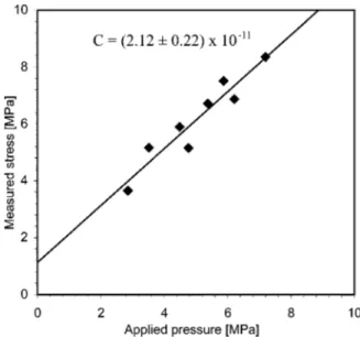
兲 = 共1−2兲 + S. 共10兲 Using this result and Eq.(4) we can determine the photoelas-tic coefficient by adjusting it in order to get a unitary slope on the plot共1⬘
−2⬘
兲 versus applied stress S. Figure 3 shows the variation of the measured stress as a function of the ap-plied stress. The experimental estimation for the photoelastic coefficent for this particular crystal orientation is共2.12±0.22兲⫻10−11Pa−1.
Since the orientation of the crystal is known, we can use Eq.(7) to compute the expected photoelastic coefficient. We find that the photoelastic coefficent is C =共2.121±0.015兲
⫻10−11Pa−1, which is remarkably consistent with the esti-mated value.
B. Multicrystalline silicon ribbons
The SCIP method was used to measure the stress distri-bution in multicrystalline silicon ribbons produced using a method developed in our laboratory and described elsewhere.4 The samples were 100 mm long and 30 mm wide. Typical tickness was 300m. Measurements were taken with a 0.3 mm resolution and with five different exter-nal stresses, in the range 0.90− 1.90 MPa. This stress range FIG. 2. Setup for measurement of the applied stress.
FIG. 3. Measured stress as a function of applied stress on monocrystalline sample.
was sufficient to determine the residual stress in our samples while avoiding sample breakage. However, this may become a limiting a factor for thinner wafers.
Figure 4 shows the variation of the measured stress with the applied stress on a multicrystalline silicon sample, for typical points in the edge and central regions on the sample. One can see that the variation of the measured stress is quite linear with the applied stress. Furthermore, one ought to no-tice that in the central region[Fig. 4(b)] the absolute value of the measured stress decreases with increasing the applied stress, which means that that region is under tension. On the other hand, in the outer area[Fig. 4(a)] the measured stress increases with the applied stress, thus suggesting that the regions near the edges of the sample are under compressive residual stress. This result is consistent with thermoelastic models18 and stress measurements using shadow moiré interferometry.19
Figure 5(a) shows the typical variation of the measured
isoclinic parameter,n, along a transversal line(i.e., perpen-dicular to the growth direction) of the sample. It is clear that the principal orientations of the refractive indices共n兲 vary from around 0–10° in the regions near the edges to around 70–90° in the central region. Using Eq.(8), we can compute the principal orientation of the residual stress, [Fig. 5(b)]. The principal orientation of the residual stress varies abruptly from values very close to 0° in the regions near the edges of the ribbon to very close to 90° in the central region. According to the thermal stress parabolic model pro-posed by Gurtler,20 silicon ribbons are expected to show
兩1兩Ⰷ兩2兩 everywhere except in the regions where 1 ap-proaches zero, i.e., at 14 and43 of the length. The variation of can then be interpreted as another evidence for tensile stress in the central region and compressive stress at the edges of the ribbons. Figure 6 shows the variation of the residual stress and the variation of the photoelastic coeffi-cient, determined using the method described in the previous section, along the same transversal line.
FIG. 4. Measured stress as a function of applied stress on multicrystalline sample for typical points in the (a) edge and (b) central regions of the sample.
FIG. 5. (a) Isoclinic parameter and (b) principal orientation of the residual stress. Typical distributions along a line perpendicular to the growth direc-tion of a multicrystalline silicon ribbon.
The residual stress distribution shows the basic features of the predictions of the parabolic model, in particular maxi-mum compressive stress is concentrated in the regions near the edges of the ribbon while the central region is under tensile stress. Furthermore, the residual stress becomes neg-libible at 14 and 34 of the length of the sample.
The distribution of residual stress is correlated to grain and twin boundaries[Fig. 6(a)]. This result is consistent with stress measurements in EFG silicon ribbons and tri-crystal silicon carried out by Möller and co-workers,21 who have associated local high stresses with high density of single slip dislocations that accumulate near grain and twin boundaries. Since the photoelastic coefficient depends on the crystal orientation, it was expected that it would be constant for each grain, while varying stepwise from grain to grain. Instead, we have observed that the photoelastic coefficient varies within each grain, reaching local maxima in the grain bound-aries[cf. Fig. 6(b)]. This result could indicate that the accu-mulation of dislocations or other defects near grain
bound-aries strongly affects the photoelastic coefficient.
Figure 6(b) also shows unexpectedly large photoelastic coefficients in the region 5 – 11 mm, a region where1−2 is small. Furthermore, the applied stress versus measured isocromatic parameter curve has an unusual nonlinear behav-ior in this region. This suggests that defective material shows an enhanced photoelastic response at low stresses that is only visible where residual stress is small.
Excluding these regions where the photoelastic coeffi-cient is very large, the average photoelastic coefficoeffi-cient is 2.0⫻10−11Pa−1 and its variation is about ±1.1⫻10−11Pa−1 which is relatively consistent with the results discussed in Sec. III.
C. Comparison with x-ray diffraction measurements
In order to validate the SCIP method, the residual stress of several silicon ribbons was measured by x-ray diffraction using an asymmetric geometry in chosen individual grains. This method will be described in detail elsewhere.22The re-sidual stress, determined from the measured deformation of the unit cell, was shown to be compressive in the outer areas while under tensile stress in the central region.
The results of the x-ray diffraction method cannot be compared directly with the photoelastic measurements since that method only yields the normal components of the stress tensor, not the tangential ones. Thus, we are not able to com-pute the principal components of the residual stress tensor. However, since we know that the principal orientation of the stress is(almost) everywhere either 0° or 90°, we can assume that the normal components are the principal components. We can then determine the principal stresses by simply changing from the crystal coordinate system共a,b,c兲 to the laboratory coordinate system共x,y,z兲:
a=1cos2,
b=1cos2, 共11兲
c=1cos2,
where , , and are the orientation angles of the (100) plane around the xx, yy, and zz axis, respectively, measured from a lauegram of the sample.
Table II shows the comparison between the measured residual stress obtained by x-ray diffraction and by the SCIP method. It is noticeable that the error bars for the x-ray mea-surement are quite large. From these results we can conclude TABLE II. Comparison between x-ray diffraction and SCIP stress measure-ments. Diffraction SCIP Sample 1 (MPa) ±␦1(MPa) 1 (MPa) ±␦1(MPa) A1 −3.30 ±1.14 −1.12 ±0.02 A2 5.05 ±3.68 4.78 ±0.10 B1 −2.64 ±1.31 −3.07 ±0.06
FIG. 6.(a) Residual stress and (b) estimated photoelastic coefficient. Typi-cal distributions along a line perpendicular to the growth direction of a multicrystalline silicon ribbon.
that the measurement of the residual stress using the x-ray diffraction method is consistent with the SCIP measure-ments.
ACKNOWLEDGMENTS
This work was partly supported by SAPIENS and a POCTI scholarship.
1
J. P. Kalejs, in Silicon Processing for Photovoltaics, edited by C. P. Khat-tak and K. V. Ravi(Elsevier, Amsterdam, 1987), Vol. II.
2
A. Eyer, N. Schillinger, S. Schelb, A. Räuber, and J. G. Grabmaier, J. Cryst. Growth 82, 151(1987).
3
K. M. Kim, S. Berkman, H. E. Temple, and G. W. Cullen, J. Cryst. Growth 50, 212(1980).
4
J. M. Serra and A. M. Vallera, Proceedings of XXI IEEE Photovoltaic Specialists Conference, Orlando, FL, 1990, pp. 615–617.
5
H. Ghitani and S. Martinuzzi, J. Appl. Phys. 66, 1717(1989).
6
B. J. Sloan and J. R. Hauser, J. Appl. Phys. 41, 3504(1970).
7
S. R. Lederhandler, J. Appl. Phys. 30, 1631(1959). 8
R. O. DeNicola and R. N. Tauber, J. Appl. Phys. 42, 4262(1971). 9
D. Chambonnet, R. Gauthier, and P. Pinard, Rev. Sci. Instrum. 57, 2806
(1986).
10
E. M. Gamarts, P. A. Dobromyslov, V. A. Krylov, S. V. Prisenko, E. A. Jakushenko, and V. I. Safarov, J. Phys. III 5, 1033(1993).
11
E. A. Patterson and Z. F. Wang, Strain J. Brit. Soc. Strain Measurement 27, 49(1991).
12
T. Zheng and S. J. Danyluk, J. Mater. Res. 17, 36(2002). 13
J. F. Nye, Physical Properties of Crystals(Oxford University Press, Ox-ford, 1972).
14
H. Liang, Y. Pan, S. Zhao, G. Qin, and K. K. Chin, J. Appl. Phys. 71, 2863(1992).
15
K. Ramesh and V. Ganapathy, J. Strain Anal. 31, 423(1996).
16
J. Maia Alves, M. C. Brito, J. M. Serra, and A. M. Vallera, Rev. Sci. Instrum.(accepted).
17
R. G. Budynas, Advanced Strength and Applied Stress Analysis(McGraw– Hill, New York, 1977).
18
J. P. Kalejs, B. H. Mackintosh, and T. Surek, J. Cryst. Growth 50, 175 (1980).
19
Y. Kwon, S. Danyluk, L. Bucciarelli, and J. P. Kalejs, J. Cryst. Growth 82, 221(1987).
20
R. W. Gurtler, J. Cryst. Growth 50, 69(1980).
21
H. J. Möller, C. Funke, A. Lawerenz, S. Riedel, and M. Werner, Sol. Energy Mater. Sol. Cells 72, 403(2002).
22
J. Pereira, M. C. Brito, J. Maia Alves, J. M. Serra, A. M. Vallera, A. Sequeira, and N. Franco(unpublished).