Dielectric properties of BaTiO
3
(BTO)–CaCu
3
Ti
4
O
12
(CCTO) composite
screen-printed thick films for high dielectric constant devices in the
medium frequency (MF) range
A.F.L. Almeida
a, P.B.A. Fechine
a, J.C. Góes
b, M.A. Valente
c, M.A.R. Miranda
d,
A.S.B. Sombra
b,∗aDepartamento de Quimica Orgˆanica e Inorgˆanica-UFC, Ceará, Brazil
bDepartamento de F´ısica, Laboratório de Telecomunicações e Ciˆencia e Engenharia dos Materiais (LOCEM),
Universidade Federal do Ceará, Caixa Postal 6030, Fortaleza CEP 60455-760, Ceará, Brazil
cDepartamento de F´ısica, Universidade do Aveiro, Portugal
dLaboratório de raios-X, Departamento de F´ısica UFC Campus do Pici, Caixa Postal 6030, CEP 60, 455–760 Fortaleza, CE, Brazil
Received 1 September 2003; accepted 24 March 2004
Abstract
In this paper, we will study the effect of the presence of CCTO (CaCu3Ti4O12) in the dielectric permittivity and loss of barium titanate
(BTO-BaTiO3) thick films. These films were prepared in two layers geometry using the screen printing technique on Al2O3 substrates.
Mechanical alloying followed by the solid state procedure has been used successfully to produce powders of CCTO (CaCu3Ti4O12) used in
the films. We also look at the effect of the grain size of the BTO and CCTO in the final properties of the film. These samples were studied using X-ray diffraction, scanning electron microscopy (SEM), Raman and infrared spectroscopies. We also did a study of the dielectric permittivity (K) and loss (D) in the medium-frequency (MF) range (100 Hz–1 MHz), of the films. The role played by firing process in the film preparation and the crystallite size of CCTO and BTO in the dielectric constant and structural properties of the films are discussed. Therefore, these measurements confirm the potential use of such materials for small high dielectric planar devices. These films are also attractive for capacitor applications and certainly for microelectronics, microwave devices (cell mobile phones, for example), where the miniaturization of the devices is crucial.
© 2004 Elsevier B.V. All rights reserved.
Keywords: Ferroelectrics; Screen printing; Thick films
1. Introduction
Ferroelectric thin films of thickness below 1m have been extensively investigated due to their potential applications in microelectronics and micromechanics. However, less at-tention has been directed to processing of thicker films. A reasonable number of applications require films of several microns to several tens of microns. Whereas ferroelectric thin films methods have their specific features, ferroelectric thick films processing is closer to that of the bulk ceram-ics, including powder synthesis, powder processing, coating
∗Corresponding author. Fax:+55-8-5287-4138.
E-mail address: [email protected] (A.S.B. Sombra). URL: http://www.locem.ufc.br.
and sintering. Coating is obtained by screen printing, a well developed processing step in thick film technology.
Applications of ferroelectric thick films includes pyro-electric sensors[1,2], gravimetric sensors[3], micropumps [4], pressure sensors[5], and surface acoustic wave sensors (SAW)[6]devices. Properties obtained are poorer compared to the bulk ceramics due to the addition of low temperature sintering aids and/or high porosity.
Most multichip modules (MCMs) fabricated today re-quire decoupling capacitors to suppress the power distribu-tion noise[7,8]. These surface mount capacitors are large in size, occupy space, and have large parasitic capacitance. Materials with relative dielectric constant (K) in the range of 25–170 are required for advanced decoupling capacitors. In this paper we will study a composite thick film with two different phases. The first ceramic will be barium titanate
(BaTiO3–BTO), a well known ferroelectric material, has a high dielectric constant (K) around 6.000 at a fine grain size of∼1m, and of 1500–2000 at a coarse grain size[9,10]. The dielectric constant of BTO at the Curie temperature of 120◦C can reach a peak value as high as 10.000, but decreases as the temperature decreases. Chemical additives or so called shifters have been applied to BTO to move the Curie peak value towards room temperature to improve the dielectric constant, and to smooth the Curie peak to obtain a lower temperature coefficient of the K value.
Dielectric properties of BTO ceramics are highly depen-dent upon the grain size, phase content of the ceramic body and also the type of dopants used. For BTO powder, its be-havior is also related to the particle size, phase content, and the dopants added. Cubic BTO (c-BTO) powder transforms to the tetragonal phase (t-BTO) if its size is larger than 30 nm[11]. Powder with a size of 40–80 nm contains a sin-gle domain. Crystallites with a size larger than 80 nm will be multidomain t-BTO[12]. The increase of the dielectric constant is possibly caused by a summation of the domain size and the stress effect[13]. It is also mentioned that the width of ferroelectric 90◦ domains decreases proportional to the square root of the grain diameter for grains with size <10m[13]. The removal of grain boundaries, i.e. elimi-nation of constrained forces from neighboring grains and a drop in domain density as the particle size decreases, may reduce the DC of the BTO powders. With increasing particle size, unsintered powder eventually becomes a ceramic-like body and possesses similar properties as the ceramics[14]. Therefore, ceramics and powders of BTO can show a dif-ferent dielectric behavior, depending on the particle size.
The second crystalline phase will be in the form of CaCu3Ti4O12 (CCTO)[15–17]. For this material, high di-electric constants have been found which shows a didi-electric constant at 1 kHz of about 10.000 that is nearly constant from room temperature to 300◦C. Oxides with the per-ovskite structure are well stabilised by their high dielectric constants (K) which lead these class of materials to a big number of technological applications [15]. However, this behavior is generally associated to ferroelectric or relaxor properties. In these cases the highest value of K is obtained during a phase transition (as a function of temperature) presented by the material.
The existence of the transition temperature event is gen-erally a problem when one is talking about applications of these materials. The reported results for CCTO shows that the K is high but with small dependence on the temperature [16].
Such material is very promising for capacitor applications and certainly for microelectronics, microwave devices (cell mobile phones for example), where the miniaturization of the devices are crucial.
High K ceramics make it possible to noticeably miniatur-ize passive microwave devices. Their sminiatur-ize can typically be reduced in comparing with classical resonators and filters by a factor of√K(relative dielectric constant). The structure
of CCTO was previously determined from neutron powder diffraction data[17]. It belongs to space group Im3 (No. 204) [17]. Recently, we propose the use of mechanical alloying to produce CCTO[18]. The mechanical alloying is proving to be a powerful technique to obtain any quantity of powder with controlled microstructure [19]. Recently, a polymeric citrate precursor route was used to produce CCTO[20]. It was observed dielectric constant of 3.000 and loss around 0.3–0.35 at 1 kHz.
In this work we report the preparation of the ceramic of CCTO through the solid state route and use this mate-rial together with commercial BTO to prepare a composite thick film. The produced samples were studied using X-ray diffraction, infrared and Raman spectroscopy and scanning electron microscopy (SEM) techniques. The dielectric con-stant and loss were also studied in the range of 100 Hz to 1 MHz. The production, and the study of the properties of the BTO–CCTO thick films is important in view of possible applications as bulk devices like microwave resonators and oscillators, thick and thin high K films.
2. Experimental methods
2.1. CCTO crystalline powder
Commercial oxides Ca(OH)2 (Vetec, 97% with 3% of CaCO3), titanium oxide (TiO2) (Aldrich, 99%), CuO (Aldrich, 99%) were used in the CCTO preparation. The material was ground on a Fritsch Pulverisette 6 planetary mill with the proportionality of Ca(OH)2–3CuO–4TiO2. Milling was performed in sealed stainless steel vials and balls under air. Mechanical alloying was performed for 30 min of milling. In this case the milling was used only to give a good homogeneity of the powder. However, we already showed in the literature that for 100 h of milling the complete production of CCTO is possible [18]. The reaction occurring during milling can be summarized as:
Ca(OH)2+3CuO+4TiO2 impacts
−−−→CaCu3Ti4O12+H2O The compounds were also prepared by the conventional powder-sintering technique using the same starting materi-als. The ceramic was submitted to calcination and sintering in air in the range of 900–1100◦C for 12–24 h [17]. This ceramic is called CCTOCS (calcination+sintering).
2.2. BTO powder preparation
The used BTO powder was a commercial product (BaTiO3-Aldrich). This ceramic is called BTOC (commer-cial)
2.3. Paste preparation
im-Fig. 1. A rectangular coordinate assigned to the sample for the measure-ment of electric premittivity and loss of the thick film structure.
prove rheological behavior of the paste) and powders (BTO, CCTO, BTO50-CCTO50). To have a better adhesion be-tween paste and substrate (Al2O3) it was added a low tem-perature melting material in powder form (flux material).
2.4. Substrates and electrodes
Alumina substrates were used as a commercial product (Engecer). The electrode material were produced for the screen printing technique (Joint Metal-PC200) in the geom-etry described inFig. 1.
2.5. Preparation of the films
The bottom electrodes (Ag) was screen printed on the Al2O3 substrate and fired at 850◦C for 1 h. On the fired electrode, a first layer was screen printed and sintered at for 1 h. After firing the dielectric layer, the upper electrode (Ag) was deposited, and after that dried and fired at the same temperature-time regime as for the bottom electrode. The obtained films usually had thickness that ranged from 20 to 400m, depending on the number of layers. All the films used in these measurements were composed of two layers.
In this paper one has three types of films: BTO100 (100% BTO thick film), CCTO100 (100% CCTO thick film) and BTO50-CCTO50 (in this film one has 50% of each compo-nent in the film) where the percentage is given in wt.%.
The film was subjected to the firing process:
100◦C for 1 h +400◦C for 1 h +900◦C for 1 h (first layer).
100◦C for 1 h+400◦C for 1 h+900◦C for 4 h (second layer).
2.6. X-ray diffraction
The X-ray diffraction (XRD) patterns were obtained at room temperature (300 K) by step scanning using powdered samples. We used five seconds for each step of counting time, with a Cu K␣tube at 40 kV and 25 mA using the ge-ometry of Bragg-Brentano. The analysis of the crystallite size (Lc) of the HA phase has been done for all samples using the Scherrer’s equation[28]
Lc= kλ βcosθ
where k is the shape coefficient (value between 0.9 and 1.0), λthe wave length,β the full-width at half-maximum (FWHM) of each phase andθthe diffraction angle. For this purpose, we chose the single peak near 56.3◦ within the pattern and according to the space group of BTO and 34.8 for CCTO. We have used the LaB6 (SRM 660—National Institute of Standard Technology) powder standard pattern to determine the instrumental width (winst =0.087◦) and afterward to calculate the crystallite size viaEq. (1). Theβ parameter has to be correct using the following equation:
β=
w2
exp−w2inst
wherewexpcorrespond to experimental FWHM obtained for each sample. The crystallite size for the milled ceramic and for the film was obtained, assuming coefficient k=1.
2.7. Scanning electron microscopy
The photomicrograph of the films of BTO+CCTO, were obtained on a scanning electron microscope, Phillips XL-30, operating with bunches of primary electrons ranging from 12 to 20 keV, in rectangular lyophilized samples, covered with a layer of carbon of 30 nm of thickness.
2.8. Dielectric measurements
2.9. Infrared spectroscopy
The infrared spectra (IR) were measured using KBr pel-lets made from a mixture of powder for each glass compo-sition. The pellet thickness varied from 0.5 to 0.6 mm. The IR spectra were measured from 400 to 1200 cm−1 with a Nicolet 5ZPX FT-IR spectrometer.
2.10. Raman spectroscopy
Micro-Raman measurements were performed using a T64000 Jobin Yvon spectrometer equipped with an N2-cooled charge coupled device (CCD) to detect the scat-tered light. The spectra were excited with an argon-ion laser (5145 Å). The spectrometer slits were set to give a spectral resolution always better than 2 cm−1. The Raman scattering was measured in a back scattering geometry directly from the powder.
3. Results and discussion
3.1. X-ray diffraction
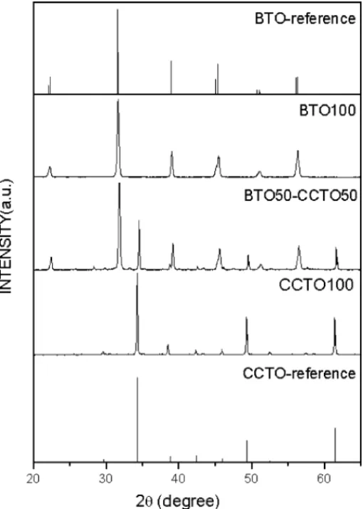
Fig. 2 shows the X-ray diffraction (XRD) patterns of the films BTO100, CCTO100 and BTO50-CCTO50 to-gether with the XRD of the references (JCPDS), that were used in the film preparation (as discussed before). In the same figure one starts with the XRD of sample BTO100. For this film one can easily identify all the peaks associ-ated to BTO. However, the crystallite size associassoci-ated to BTO is around 36.6 nm (see Table 1). One can associate the increase of the grain size to the firing process that the film was submitted. Extra peaks associated to the flux material was not detected (the flux material was used to improve the adhesion between the paste and the substrate). For sample BTO50-CCTO50 the presence of BTO and CCTO is easily identified and for the film CCTO100, the presence of CCTO is quite clear. Initially the crystallite size of the BTO increases from 26 to 36.6. The CCTO crystallite size is bigger when compared with the crystal-lite size in BTO. For the kind of films under study, the
Table 1
Dielectric permittivity (K), thickness (e), dielectric loss (D), and the crystallite size obtained from the X-ray diffraction (Fig. 2) of the thick films and powders (electrode diameter, L=1 cm, seeFig. 1)
Samples Thickness e (m)
Kε33′/ε0 1 kHz
Dε33′′/ε33′ ×10−2 1 kHz
Crystallite size (nm)
Ba/Ti mass ratio
Ca/Cu mass ratio
Ca/Ti mass ratio
Cu/Ti mass ratio Starting ceramics
BTOC 26
CCTOCS 154.4
Thick films
BTO100 142 592 1 36.6 1.27 (2.87)
BTO50-CCTO50 147 1304 5 43.7 0.849 (0.57) 0.27 (0.21) 0.06 (0.17) 0.21 (0.8)
CCTO100 135 403 31 76.5 0.19 (0.21) 0.20 (0.21) 1.07 (1.0)
Mass relation Ba/Ti, Ca/Cu, Ca/Ti and Cu/Ti obtained from energy dispersive spectroscopy [experimental value, (theoretical value)].
Fig. 2. X-ray diffraction of the films BTO100, BTO50-CCTO50, CCTO100 Joint Committee on Powder Diffraction Standards (JCPDS); International Center for Diffraction Data; 12 Camous Blvd.; New-ton Square; Pennsylvania 19073-3723; USA; 19995—Pattern 93-1880 [BTO-reference], 75-1149 [CCTO-reference].
CCTO film present the highest value for the crystallite size (76 nm).
3.2. Scanning electron microscopy
Fig. 3. Scanning electron photomicrograph of BTO100 thick film (7000×).
Fig. 5. Scanning electron photomicrograph of the CCTO100 thick film (7000×).
BTO50-CCTO50 and CCTO100, respectively. ForFigs. 3–5 one has an amplification of 7000× for the same samples. ComparingFigs. 3 and 4one can notice that the scanning electron photomicrograph of the films revealed a spherical morphology for the synthesized particles of BTO in these films. InFigs. 4 and 5one can notice the presence of CCTO grains. These grains are bigger compared with the BTO grains. This is confirmed when one comparesFigs. 5 and 3. Comparing the three films, one can notice that the presence of CCTO in the film is increasing the presence of micro-craks which is less intense in the BTO100 film compared to the CCTO100 film. Energy-dispersive spectroscopy (EDS) analysis (Fig. 6andTable 1) showed that the main elements of the BTO100 were carbon, oxygen, barium and titanium. For the BTO50-CCTO50B film one has to include copper and calcium phosphorus. For the CCTO100 film one has copper, titanium, oxygen and calcium. The EDS of a crys-tal, present in the BTO100 film showed a mass ratio Ba/Ti
=1.27 (Fig. 6,Table 1), whereas it is Ba/Ti=0.85 for the BTO50-CCTO50. We have to compare this value to Ba/Ti
=2.87 for the nominal BTO. This is half of the expected value for the first sample and even lower for composite sample. We believe that for the first sample (BTO100) the BTO used is presenting an excess of Ti in the structure. Ex-cess of TiO2, in BTO preparation, results in the formation of separate phases like Ba6Ti17O4and this forms a eutectic with BTO[21]. However, the presence of others phases in
the BTO used was not detected (seeFig. 2). For the second film BTO50-CCTO50 this ratio is even lower, probably be-cause of the presence of titanium in the CCTO phase, which could lead to a decrease of the ratio. For the CCTO100 film the ratio Ca/Cu is around 0.19 which is quite close to the expected value which is 0.21 (seeTable 1).
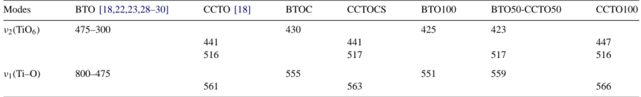
3.3. Infrared spectroscopy
In Fig. 7 and Table 2 one has the infrared spectra from the ceramics CCTOCS and BTOC and the films BTO100,CCTO100 and BTO50-CCTO50. The IR spectra of the BTOC ceramic in the region of 400–1200 cm−1 is dominated by two broad absorptions centered at 555 and 430 cm−1. A similar spectrum is observed for the film BTO100, with absorptions at 551 and 425 cm−1(seeFig. 7). The absorptions associated to BTO are υ1 (Ti–O vibra-tions), TO mode attributed to the stretching mode of TiO6 octahedron variety of the 800–475 cm−1 and υ
Fig. 6. Energy dispersive spectroscopy of the thick films BTO100, BTO50-CCTO50, CCTO100.
broad bands associated to the BTO spectra. In summary one can say that the main bands associated to BTO and CCTO were identified in the films according with data from the literature.
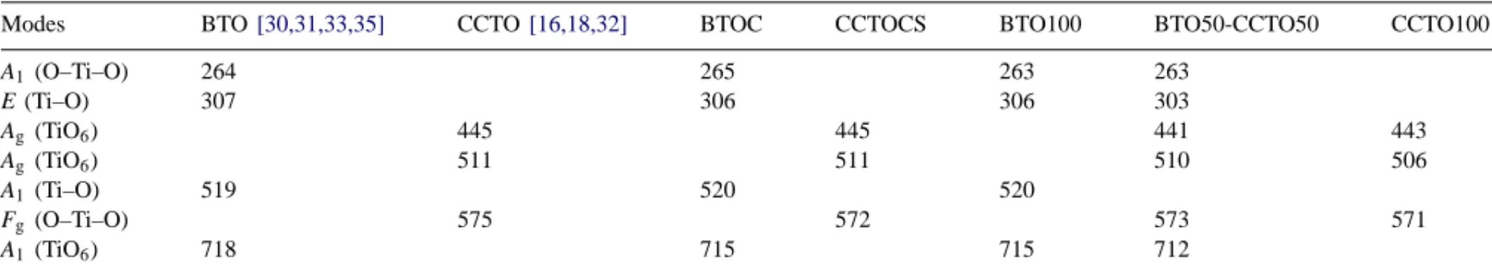
3.4. Raman spectroscopy
In Fig. 8one has the Raman spectra of the original ce-ramics used in the film preparation, BTOC and CCTOCS, and the films BTO100, CCTO100 and BTO50-CCTO50. The Raman spectra of the CCTO calcined and sintered sam-ple (CCTOCS) one has three main peaks at 445, 511 and 572 cm−1 (see Fig. 8) in good agreement with values re-ported in the literature[16,18,33]. The Raman lines (Table 3)
Table 2
Infrared modes (cm−1) of the films BTO100, CCTO100, BTO50-CCTO50 and the ceramics BTOC and CCTOCS
Modes BTO[18,22,23,28–30] CCTO[18] BTOC CCTOCS BTO100 BTO50-CCTO50 CCTO100
ν2(TiO6) 475–300 430 425 423
441 441 447
516 517 517 516
ν1(Ti–O) 800–475 555 551 559
561 563 566
Fig. 7. Infrared spectra of the films BTO100, CCTO100, BTO50-CCTO50 compared with the IR of the starting materials (BTOC, CCTOCS).
at 445 and 511 cm−1have Agsymmetry (TiO6rotationlike). The peak at 572 cm−1is associated to a mode of Fg symme-try (O–Ti–O antistretching).
The Raman spectra of the BTO commercial film (BTOC) has four main peaks (Fig. 8). We clearly observed four peaks at the following frequencies: at 265, 306, 520 and 715 cm−1. The wide peak at 265 cm−1is attributed to a A
1(LO) mode. The band at approximately 715 cm−1 is associated with the highest frequency LO mode of A1symmetry. The sharp peak located at 306 cm−1is associated[34–36]to the E(TO
+LO) mode.
Fig. 8. Raman spectra of the films BTO100, CCTO100, BTO50-CCTO50 compared with the Raman of the starting materials (BTOC, CCTOCS).
at 520 cm−1 is assigned to the A
1(TO) mode. The Ra-man modes of the samples BTO100 and CCTO100 are in good agreement with the values reported in literature [16,18,30,31,33–36], see Table 3. These values were also observed for the BTO50-CCTO50 film.
For the composite film (BTO50-CCTO50) one can eas-ily identify the four modes associated to the BTO presence at 263, 303, 510 and 712 cm−1. The modes associated to the CCTO are coincidente with the band at 520 cm−1
as-Table 3
Raman modes (cm−1) of the films BTO100, CCTO100, BTO50-CCTO50 and the ceramics BTOC and CCTOCS
Modes BTO[30,31,33,35] CCTO[16,18,32] BTOC CCTOCS BTO100 BTO50-CCTO50 CCTO100
A1 (O–Ti–O) 264 265 263 263
E (Ti–O) 307 306 306 303
Ag (TiO6) 445 445 441 443
Ag (TiO6) 511 511 510 506
A1 (Ti–O) 519 520 520
Fg (O–Ti–O) 575 572 573 571
A1 (TiO6) 718 715 715 712
Fig. 9. Dielectrc permittivity (K) as a function of frequency of the films BTO100, CCTO100, BTO50-CCTO50.
sociated to BTO. However, peaks at 441 and 573 are still detected.
3.5. Dielectric measurements
dielec-Fig. 10. Dielectrc loss (D) as a function of frequency of the films BTO100, CCTO100, BTO50-CCTO50.
tric constant is higher for all the frequencies under study. At 1 kHz the value of the K is around 1304. Which is more than two times bigger compared to the BTO100 value for a less thicker film (see Table 1) The other point is that for CCTO100 and for BTO50-CCTO50 there is a tendency do decrease of K with the increase of the frequency from 100 Hz to 1 MHz. This behavior is less accentuated for the BTO100 film.
In Fig. 10one has the dielectric loss for these films. At 1 kHz the loss is higher for the CCTO100 film (0.31). When one decrease the amount of CCTO in the film, there is a decrease of the loss. It decrease for the BTO50-CCTO50 (0.05) and is the lowest for the BTO100 film (0.01). The presence of BTO in the film lead to a tendency of increasing the loss with frequency which is observed for the BTO100 and BTO50-CCTO50 films in the range of studied frequen-cies (seeFig. 10).
This amazing behavior observed for the composite film is probably associated with the sizes of the grains in both phases and to the interface between these grains. We are now looking the presence of this effect in the microwave region as well.
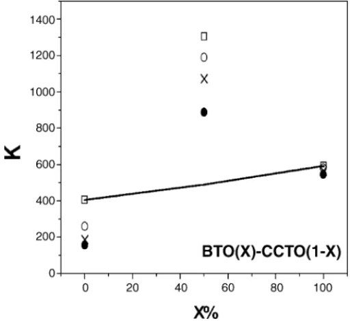
The classic treatment applied for two or more phases present in a dielectric are associated to the dielectric mixing rules that fix a limit to the dielectric constant that can be achieved with the mixed phase. The empirical logarithmic rule for the dielectric constant K and the dielectric constants
Fig. 11. Dielectric permittivity for the medium frequency range. Continuos line obtained from Eq. (1) (f =1 kHz). Experimental points extracted fromFig. 9. For 1 kHz (䊐), 10 kHz (䊊), 100 kHz (×), 1 MHz (䊉). (KI) of the individual phases is given by[36]
logK=
I
VIlogKI (1)
In Fig. 11 one has the plot of the dielectric constant as a function of the substrate composition for the MF region and for several frequencies, based inEq. (1).
The continuous line are associated to the value of K ob-tained fromEq. (1), at 1 kHz.
The experimental points (for the frequencies 1, 10, 100 kHz and 1 MHz) of the samples are also indicated in the figure. One can easily conclude that the addition of BTO is increasing the K of the substrate at 1 kHz of fre-quency. However, for x =50% the experimental value of the dielectric constant is much higher when (average value of K ∼ 1304) compared to the expected value suggested by Eq. (1) (K ∼ 488.6) at 1 kHz. This is an unexpected behavior. It means that the composite is not following the linear regime of the model. This behavior is present in all the studied frequencies (medium frequency (MF) range) (see Fig. 11). In summary, three different substrates of BTO100, CCTO100 and BTO50-CCTO50 were studied in the medium frequency range of the spectra.
loss for the sample BTO50-CCTO50 is higher compared to the BTO100 and CCTO100 samples.
One can say that the BTO100 film is presenting a higher value of K at 1 kHz (592) compared to the CCTO100 film (403). However, for the composite film BTO50-CCTO50 is presenting a surprising effect where the composite ceramic is not following the linear dielectric model with a K value around 1304 (seeFig. 11) which seems to be a nonlinear mixing effect of the two phases.
4. Conclusions
In this paper we did a study of the effect of the presence of CaCu3Ti4O12(CCTO) in the dielectric and optical prop-erties of the barium titanate BaTiO3(BTO) thick film. The films were prepared in two layers using the screen print-ing technique on Al2O3substrates. Mechanical alloying fol-lowed by the solid state procedure has been used success-fully to produce powders of CaCu3Ti4O12 (CCTO) to be used in the films. We also look at the effect of the grain size of the BTO and CCTO in the final properties of the film. The samples were studied using X-ray diffraction, SEM, Ra-man and infrared spectroscopy. We also did a study of the dielectric function K and dielectric loss of the samples.
The X-ray diffraction (XRD) patterns of the films indicate that all the peaks associated to BTO phase is present in the films in the tetragonal phase, which is in agreement with the Raman spectroscopy data. One can also notice an increase of the crystallite size associated to the firing process for the BTO film. The CCTO crystallite size is bigger when compared with the crystalline size in BTO. For the kind of films under study, the CCTO film presents the highest value for the crystallite size (76 nm).
The particle morphology of the films was investigated by means of SEM. For the BTO films and composite films a spherical morphology was observed for the synthesized particles. One also notice that the CCTO grains are bigger compared with the BTO grains. However, one can notice that the presence of CCTO in the film is increasing the presence of microcraks which is less intense in the BTO100 film compared to the CCTO100 film.
The main Infrared absorptions and Raman modes asso-ciated to BTO and CCTO are observed, in good agreement with the X-ray analysis. The IR spectra of the BTOC ceramic in the region of 400–1200 cm−1is dominated by two broad absorptions centered at 555 and 430 cm−1. Similar spectra is observed for the film BTO100, with absorptions at 551 and 425 cm−1. For the CCTOCS ceramic three main absorp-tions were observed at 563, 517 and 441 cm−1which is also observed for the CCTO100 film at 566, 516 and 447 cm−1. For the composite film one has a mixing of each absorption spectra.
The main Raman modes associated to BTO and CCTO were observed. The Raman spectra of the CCTO calcined and sintered sample (CCTOCS) has three main peaks at 445,
511 and 572 cm−1in good agreement with values reported in the literature[1–3]. The Raman spectra of the BTO com-mercial film (BTOC) has four main peaks at the following frequencies: at 265 cm−1, 306, 520 and 715 cm−1.
The BTO100 and CCTO100 samples have the modes in good agreement to the values reported in literature.
For the composite film (BTO50-CCTO50) one can easily identify the four modes associated to the BTO presence at 263, 303, 510 and 712 cm−1. The modes associated to the CCTO are coincident with the band at 520 cm−1associated to BTO. However peaks at 441 and 573 cm−1 are still de-tected.
Looking now for high K and low loss film, which is the best options for use in microwave devices like dielectric res-onators, one has to find a balance between high dielectric constant and low loss. One can notice that, the BTO film present a higher K value compared to CCTO in the range of frequencies under study. At 1 kHz the value is around 592 for the BTO100 film compared to 403 for the CCTO film. However for the composite film one has an unexpected result. The dielectric constant is higher for all the frequen-cies under study. At 1 kHz the value of the DC is around 1304. Which is more than two times bigger compared to the BTO100 value for a less thicker film The other point is that for CCTO100 and for BTO50-CCTO50 there is a tendency do decrease of the K value with the increase of the frequency from 100 Hz to 1 MHz. This behavior is less accentuated for the BTO100 film.
At 1 kHz the loss is higher for the CCTO100 film (0.31). When one decreases the amount of CCTO in the film, there is a decrease of the loss. It decreases for the BTO50-CCTO50 (0.05) and is the lowest for the BTO100 film (0.01). The presence of BTO in the film lead to a tendency of increasing the loss with frequency, which is observed for the BTO100 and BTO50-CCTO50 films in the range of studied frequencies.
Considering the classic treatment applied for two or more phases present in a dielectric and the empirical logarithmic rule for the dielectric constant K and the dielectric constants
KIof the individual phases one conclude that in the MF re-gion of the spectra, the value of the dielectric constant is not in good agreement with the rule. In a general view, the pres-ence of the composite structure of BTO50-CCTO50 is lead-ing to a strong increase of the dielectric constant of the film. We expect to find an equilibrium situation with the maximum for the dielectric constant and lower loss in the composite.
This strongly suggests that the screen-printing composite BTO-CCTO thick films are good candidates for applications where one are looking for high K materials with low loss in radio-frequency range.
Acknowledgements
and by FINEP, CNPq, FUNCAP and CAPES (Brazilian agencies).
References
[1] A. Lozinski, F. Wang, A. Uusimaki, S. Leppavouri, Meas. Sci. Technol. 8 (1997) 33.
[2] C. Lucat, F. Menil, R. Von Der Muhll, Meas. Sci. Technol. 8 (1997) 38.
[3] V. Ferrari, D. Marioli, A. Taroni, Meas. Sci. Technol. 8 (1997) 42. [4] M. Koch, N. Harris, R. Maas, A.G.R. Evans, N.M. White, A.
Brunnschweiler, Meas. Sci. Technol. 8 (1997) 49.
[5] B. Morten, G. De-Cicco, M. Prudenziati, Sens. Actuators A31 (1992) 153.
[6] N.M. White, V.T.K. Ko, Electron. Lett., August (1993) 1807. [7] P. Chahal, R.R. Tummala, IEEE transaction on components,
pack-aging, and manufacturing technology B21 (2) (1998) 184. [8] S. Bhattacharya, R.R. Tummala, P. Chahal, G. White, in: Proceedings
of the International Symposium on Advanced Packaging Materials, 1997, p. 68.
[9] K. Kinoshita, A. Yamaji, J. Appl. Phys. 47 (1976) 371.
[10] W.R. Buessem, L.E. Cross, A.K. Goswami, J. Am. Ceram. Soc. 49 (1966) 33.
[11] F.S. Yen, H.I. Hsiang, Jpn. J. Appl. Phys. 34 (1995) 6149. [12] H.I. Hsiang, F.S. Yen, J. Am. Ceram. Soc. 79 (1996) 1053. [13] G. Arlt, D. Hennings, G.J. With, J. Appl. Phys. 58 (1985) 1619. [14] H.I. Hsiang, F.S. Yen, Jpn. J. Appl. Phys. 32 (1993) 5029. [15] M.A. Subramanian, D. Li, N. Duran, B.A. Reisner, A.W. Sleight, J.
Sol. State Chem. 323 (2000) 151.
[16] A.P. Ramirez, M.A. Subramanian, M. Gardel, G. Blumberg, D. Li, T. Vogt, S.M. Shapiro, Solid State Commun. 115 (2000) 217.
[17] M.A. Subramanian, A.W. Sleight, Solid State Sci. 4 (2002) 347. [18] A.F.L. Almeida, R.S. de Oliveira, J.C. Góes, J.M. Sasaki, J. Mendes
Filho, A.S.B. Sombra, Mater. Sci. Eng. B 96 (2002) 275. [19] R.S. de Figueiredo, A. Messai, A.C. Hernandes, A.S.B. Sombra, J.
Mater. Sci. Lett. 17 (1998) 449.
[20] P. Jha, P. Arora, A.K. Ganguli, Mater. Lett. 4179 (2002) 1–4. [21] A.J. Moulson, J.M. Herbert, Electroceramics, Chapman and Hall,
1990.
[22] R. Asiaie, W. Zhu, S.A. Akbar, P.K. Dutra, Chem. Matter 8 (1996) 226.
[23] L. Preda, L. Courselle, J. Bandet, A. Ianculescu, Thin Solid Films 389 (2001) 43.
[24] J.T. Last, Phys. Rev. 105 (1957) 6.
[25] G. Busca, V.B. Uscaglia, M. Leoni, P. Nanni, Chem. Mater. 6 (1994) 955.
[26] W.G. Spitzer, R.C. Miller, D.A. Kleinman, L.G. Howarth, Phys. Rev. 126 (1962) 5.
[27] B. Lee, J. Zhang, Thin Solid Films 388 (2001) 107. [28] M. Wada, T. Ohtuki, Phys. B 219–220 (1996) 635.
[29] M.I. D´ıaz-Güemes, T.G. Carreòo, C.J. Serna, Spectrochim. Acta 45A (1989) 589.
[30] B. Wang, L.D. Zhang, L. Zhang, Y. Yan, S.L. Zhang, Thin Solid Films 354 (1999) 262.
[31] W.-S. Cho, J. Phys. Chem. Solids 59 (1998) 659.
[32] N. Kolev, R.P. Bontchev, V.N. Popov, V.G. Hadjiev, A.P. Litvinchuk, M.N. Iliev, Phys. Rev. B 66 (2002) 132102–132111.
[33] E.W. Kreutz, J. Gottmann, M. Mergens, T. Klotzbucher, B. Vosseler, Surf. Coat. Technol. 116 (1999) 1219.
[34] Q.-Y. He, X.-G. Tang, J.X. Zhang, I.-M. Wu, Nanostruct. Mater. 11 (1999) 287.
[35] C.H. Perry, D.H. Hall, Phys. Rev. Lett. 15 (1965) 700.