Corresponding author: Marcelo Andrade Macêdo, Departamento de Física, Universidade Federal de Sergipe – UFS, Bairro Rosa Elze, CEP 49100-00, São Cristóvão, SE, Brasil, e-mail: [email protected]
Deposited on the Surface of DGEBA Epoxy Resin by Ion Sputtering
José Elisandro de Andrade, Rogério Machado, Marcelo Andrade Macêdo
Programa de Pós-graduação em Física, Universidade Federal de Sergipe
Frederico Guilherme Carvalho Cunha
Programa de Pós-graduação em Ciência e Engenharia de Materiais, Universidade Federal de Sergipe
Abstract: In this work, silver atoms were deposited by ion sputtering on the surface of diglycidyl ether of bisphenol A (DGEBA) epoxy resin cured at 150 °C for 6 hours in air. The films of DGEBA and its precursors were characterized by Raman spectroscopy to identify the main functional groups and their relationship with the deposited silver atoms. Silver thin films of 5, 10, 15 and 20 nm were deposited on the epoxy resin at room temperature. Both the initial film of DGEBA and the subsequent silver thin film were analyzed by Atomic Force Microscopy (AFM) in the non-contact mode. Silver thin films were also analyzed using X-ray diffraction (XRD) at room temperature. The AFM results showed the formation of silver crystallites on the surface of DGEBA at very low coverage whereas XRD indicated that most of them had their main axis aligned to the normal of the surface. An increase in the coverage led to an increase in the grain size as indicated by AFM. However, XRD results indicated that the crystallite size remained almost constant while the appearance of peaks corresponding to other crystalline orientations suggests the coalescence of the original crystallites and an increase in size of the more dense planes, namely [111].
Keywords:Epoxy resin (DGEBA), silver nanoparticles, Atomic Force Microscopy, Raman spectroscopy, ion sputtering, X-ray diffraction.
Introduction
The study of the metallization of polymers is considered to be of the utmost importance from the point of view of fundamental science as well as from a technological standpoint since this process has been widely used in a range of products: reflectors for car headlights, CDs (storage data), protective packaging for electrical components, coating for food packaging and especially in microelectronics[1-6].
The thin film formed from metallization plays a vital role in integrated devices and circuits since the deposited films must have good adhesion, low resistivity and provide good coverage. The improvement of these characteristics has stimulated intensive research by the scientific community for decades[1-8]. In the area of
microelectronics, for example, especially regarding the processing of electronic components, there is a need to expose them to relatively high temperatures[1,2,5]. Therefore, harm to the final
product may occur if there is, for example, a breakdown of the structures or diffusion of small amounts of metal into the polymer. In this respect, many efforts have been made by researchers aiming to control the microstructure and thermal stability in the interface between metal and polymer. Such studies aim to improve adhesion of the metal in the polymer and prevent its degradation[2-6].
Besides the use of metals in the form of thin films, the use of silver has also been introduced in various materials acting as a biocide agent, such as appliances with silver films, tissues, bandages soaked in silver for burns etc[9-11]. All of these products
use composite materials in which the silver is embedded in a polymer matrix[7,8,12-15].
The technology used to conduct this type of dispersion is based on methods established by the chemical industry in most cases. From an economic and efficiency point of view, the roughness of the metallic phase in the polymer matrix is of fundamental
importance. Since it is a noble metal and very expensive, it is essential to explore the area/volume ratio to its extreme. The ideal solution for these needs is to use a nanotechnological approach.
Silver nanoparticles have an area/volume ratio that is extremely favorable for the coverage of large surface areas without the need for large quantities of metal. The formation of particle-like structures on the surface of the polymeric matrix, however, depends on a careful balance between various thermodynamic quantities to maximize efficiency and consistency.
Thus, the overall objective of this work in terms of fundamental science is to understand how the formation of these silver structures on the surface of the epoxy resin occurs. Epoxy resins have received special attention in relation to other thermosetting resins since they present a wide range of applications such as adhesives, paints and fibers[16].
Epoxy resins are synthetic resins, and their name comes from Greek: epi (on or between) and oxy (oxygen). This designation comes from the chemical form of the epoxy group where an oxygen atom attached to two carbon atoms. There are several types of epoxy resins. One of the most used is diglycidyl ether of bisphenol A (DGEBA), which is a resin based on bisphenol A, since it arises from the reaction of the molecule epichlorohydrin with bisphenol A[17].
Understanding these issues from the standpoint of fundamental science will have a strong technological impact, serving as a model for understanding the introduction of silver epoxy paints. The use of DGEBA as a substrate for silver deposition stems from its widespread applicability in areas as diverse as cooking utensils and the automotive industry. While in the former the biocide activity plays a major role, in the latter it adds value to the final product without a meaningful cost increase.
A
R
T
I
G
O
T
É
C
N
I
C
O
C
I
E
N
T
Í
F
I
C
at 917 cm–1 (asymmetric axial strain on the epoxy ring, where the
C–C bond increases) and at 1254 cm–1 (contraction of the C–O
bonds stretching for the C–O–C of the group epoxy). These bands are characteristic of the epoxy groups and the healing process; their intensities have decreased dramatically since the epoxy rings are consumed in the curing of the resin to form crosslinks[18].
From the results obtained by vibrational spectroscopy, and from the perspective of the literature found, assignments and intensities of the main vibrational modes of the Araldite GY 279 were organized in Table 1[16,19].
Figure 2 shows the vibrational spectrum of epoxy resin. Noteworthy was the presence of the band at 1002 cm–1 related to
the presence of polyamidoamine adduct (amino groups), and the decrease of bands at 917 cm–1 (asymmetric axial strain on the epoxy
ring, where the C–C bond increases) and 1254 cm–1 (contraction
of the C–O bonds stretching for the C–O–C of the epoxy cluster). The decrease of the bands related to the epoxy groups is due to the process of breaking these groups by polyamidoamine[16,19].
Experimental
Material
DGEBA (Araldite GY 279) and a hardening agent (polyamidoamine adduct – Aradur 2963) manufactured by Huntsman were used to obtain the epoxy resin. The plowed Araldite GY 279 and Aradur 2963 were analyzed using Raman spectroscopy. The dispersive Raman spectrometer model Senterra manufactured by Bruker Optik and a helium-neon laser with a wavelength of 633 nm (red) were used. By means of vibrational spectroscopy, the main functional groups involved in the curing process can be identified directly from their chemical bonds[16,18,19].
The Araldite GY 279 was mixed mechanically for 10 minutes with Aradur 2963 at 20 °C in the stoichiometric ratio 3:1 (wt./wt.), according to the manufacturer’s technical specification. The film was made of epoxy resin using the spin-coating technique (rotation was approximately 1,300 rpm for 10 seconds). Glass slides previously cleaned with sulfuric acid, hydrogen peroxide and deionized water were used as the substrate.
The films were kept for 48 hours at room temperature and then were submitted to a heat treatment at 150 °C for 6 hours, according to the methodology of Merad et al. to obtain a better degree of crosslinking[20].
AFM analysis of the film with and without heat treatment were performed using an Agilent 5500 atomic force microscope with silicon cantilever model All-In-One-Al, manufactured by Budget Sensors with spring constant and typical resonance frequency 2.7 N/m and 80 kHz, respectively, and tip radius <10 nm. Experiments were made in non-contact mode (topography and phase contrast). Gwyddion 2.10 software was used to analyze the AFM images.
After the topographic and spectroscopic characterization, layers of 5, 10, 15 and 20 nm of silver were deposited by ion sputtering on the surface of thermally treated epoxy resin. The equipment used was the sputtering ion model 108 manufactured by the Kurt J. Leske Company, attached to a Cressington monitoring system, the MTM10 Thickness Monitor. Argon gas and a silver target with 99.99% purity were used and were manufactured by the Kurt J. Leske Company. The samples were analyzed by AFM in non-contact mode.
The crystalline phases of the silver thin films were identified by X-ray diffraction measurements using Cu Kα radiation on a Shimadzu Lab XRD 6000 diffractometer operated at 40 kV/40 mA. All measurements were performed at room temperature within the range 2θ = 30-120° and at a speed of 2°/min.
Results and Discussion
Spectroscopic analysis
The spectroscopic characterization of materials provides information about the presence of certain functional groups that can strongly alter the nucleation and growth of silver nanoparticles on the film surface[5].
The assignment of the vibrational modes of a molecule as complex as the polymer under study is not an easy task due to the possible existence of overlapping vibrational modes, reflecting the convolution and/or displacement of some bands. In order to facilitate the visualization of the assignments of vibrational modes of functional groups, the structural formula of DGEBA (Figure 1) outlining the main carbon and oxygen atoms is presented, according to the work of Chike et al.[16].
Figure 2 shows the Raman spectra of Araldite GY 279 where it is possible to identify the functional groups that actively participate in the curing reaction of the resin[18-20]. The highlights are the bands
Figure 1. Structural formula of DGEBA condensed and numbered[16].
Figure 2. Raman spectrum of Araldite GY 279 and epoxy resin.
Table 1. Assignments of the Raman vibrational modes of DGEBA. The
vibrational modes and their intensities are indicated as follows: s: strong; m:
medium; w: weak; vw: very weak; sh: shoulder[16,19].
Wavenumber
(cm–1) Assignments
1609 Strong stretching of C=C bonds of the aromatic rings
1299 C–O stretching (ether groups) and C – C stretching
1254 C–O–C stretching of epoxy group
1229 s C–O stretching and phenolic C4–O2 stretching
1187s CH3/ gem-dimetil deformation and C6–C7/8 stretching
1113s Aromatic C–H stretching and in-plane deformation
917 sh
Asymmetric axial deformation of the epoxy ring, where the bond C–C increases and there is a contraction of the bonds C–O
836 Lateral vibrations of the bonds C–H
823 s Substituted aromatic
769 m C3–C2 skeletal
737 sh C3–C2 skeletal
666 m Aromatic C-H out-of-plane deformation
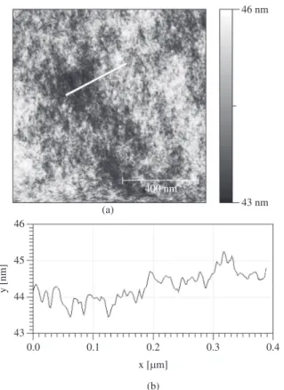
topography of the polymer is fairly regular (Figure 3a). The image of a profile (Figure 3b) was traced in the topography, which shows a small variation (of the order of 1 nm) in the surface topography of the DGEBA epoxy resin.
Metallization
Figure 4 shows the formation of layers of three-dimensional spherical clusters, after metallization, corresponding to silver nanoparticles in the sense of their plasmonic behavior; this result is consistent with the literature for other polymers[2-5,8,13,14,23]. The
images show little definition of cluster size for layers less than 5 nm, possibly due to the mobility of silver atoms on the surface of the polymer. In fact, in some experiments it was not possible to distinguish the silver from the epoxy resin, but the surface morphology is quite distinct from the sample without the thin film of silver (Figure 3a)[1,5].
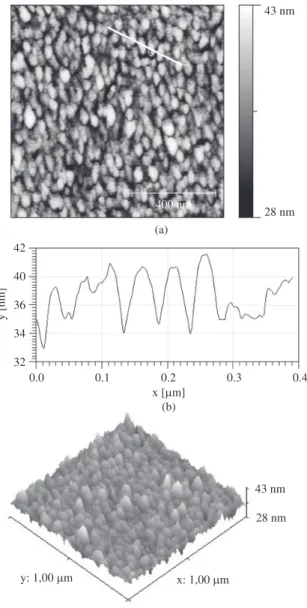
For thin films of 20 nm (Figure 5), the presence of larger clusters is shown and better defined due to the large amount of silver deposited.
Surface Analysis – AFM
The curing process of a thermoset, such as DGEBA, is not an instantaneous process. Changes in physical properties of the resin as a result of crosslinking (with the breakdown of the epoxy rings) can take hours or even days to occur. Several factors such as temperature, type of curing agent and the ratio of the reagents are among the variables that act as a catalyst[18,21].
In order to deposit the silver atoms, it is essential that the surface of DGEBA is cured, otherwise the surface will not change during the test due to the curing and/or release of volatiles (excess amine). Thus, the convolution of the effects of nucleation and growth of silver clusters with the cure of the polymer is avoided. Merad et al.[20].
have shown that the ideal cure is attained by keeping the epoxy resin at 150 °C for 6 hours giving about 80% crosslinking. The heat treatment, as well as ensuring a greater crosslinking of the polymer, ensures the release of most of the excess amine present in the polymer matrix. When heated, the resin releases a rather unpleasant odor containing carbon monoxide, carbon dioxide, nitrogen oxides and other toxic vapors and gases. A change in the color of the resin was observed at higher temperatures, ranging from transparent (without heat treatment) to yellow (heat treated)[20].
AFM surface analysis requires close attention since many factors can lead to erroneous results such as the presence of deformation or even the presence of artifacts in the image due to the tip and/or contamination. The choice of operating mode – no contact or contact – is among these important factors. In contact mode, the probe is placed in contact with the surface; in this case, the force between the tip and the sample can cause irreversible damage to the polymer and the silver thin film[22]. Thus, it is appropriate to use only
the non-contact mode in this work, since in the non-contact mode the tip is placed very close to, but not in contact with, the sample[22].
Figure 3 shows AFM images of epoxy resin. The area analyzed was 1 µm × 1 µm. It can be seen in the surface images that the
Figure 3. AFM images (topography) of epoxy resin cured at 150 °C for
6 hours (a) and profile (b). Area: 1 µm × 1 µm.
Figure 4. AFM image (topography) of a 5 nm silver thin film deposited on
Even though the images presented in Figures 4 and 5 display a clear variation on the grain size, a grain by grain measurement was performed in order to obtain a more reliable average grain size for each silver film width. Table 2 presents the result of such measurements.
As one can see, there is a continuous increase in the grain size of the silver islands on the film. To further explore this growth, XRD analysis was performed on the films. Figure 6 shows the results.
The X-ray diffraction results showed that the silver films were formed with a preferred orientation in the direction [200] with small contributions in the direction [222] and parallel plane (400). As silver is a cubic structure, it can be assumed that most of the nanoparticle-like structures are formed by crystallites in cubic faces parallel to the substrate (single crystalline). When the film is thicker than 15 nm, this preferential orientation is lost as one can see by the strong decrease in the intensity of the peak (200) and the growth of other important directions, namely [111] and [220]. In this case, the films are formed by polycrystalline grains. By using the Scherrer equation on the peak (200), the size of the crystallites on the silver thin films could be determined; these are shown in Table 2[24].
As one can verify, the crystallite diameter does not change with the film width. This remarkable result indicates that the initial growth of the small clusters is hindered by the coalescence of them into nanoparticle-like grains in the thin film surface. While the film is thin enough, the clusters owe their preferential diffraction direction to the almost flat polymer film. Both AFM and XRD indicate that this is indeed the case. As the thin film thickness increases, there is a coalescence of these clusters, or crystallites, but they do not interact in the same crystal planes. This crashing coalescence gives rise to larger grains with crystallites growing in all directions, particularly [111] as expected for a crystalline solid. The low interfacial interaction between DGEBA and the silver atoms allowed them to aggregate onto nanostructures independent of each other. Thus, clusters with greater heights than the thickness measured by the balance of quartz were formed.
Conclusions
The deposition of silver via ion sputtering on the surface of the epoxy resin DGEBA leads to the formation of silver clusters on its surface which coalesce into polycrystalline grains as the film thickness increases. The clusters formed depend on the characteristics of the deposition, especially on the thickness deposited and thermal effects. The thicker the deposited layer, the larger the grain size and the easier identification by AFM will be. In the initial steps of the film formation, the silver atoms aggregate into small clusters, or crystallites, that preferentially grow in the direction normal to the polymer surface, giving rise to the appearance of a clear peak in the [200] direction. Once these crystallites no longer find space to grow along this direction, a vertical growth ensues leading to the appearance of the characteristic diffraction pattern of polycrystalline silver. It is worth noting that the film thickness, measured at the ion-sputtering chamber, reflects the amount of mass deposited onto the surface. The high surface atom’s mobility and slow deposition
Figure 5. AFM image (topography) of a 20 nm silver thin film deposited on
DGEBA (a), profile (b) and 3D (c). Area: 1 µm × 1 µm.
Figure 6. XRD diffraction pattern of thin silver films deposited on DGEBA.
Table 2. Average grain diameter for the silver thin films as a function of the
silver film width (as obtained by AFM) and crystallite diameter as a function of the silver thin film width (as obtained by XRD). All XRD data is taken in the peak [200].
Film Width
(nm) Size (nm)
Crystallite diameter (nm)
5 31 ± 9 33.3
10 37 ± 6 32.1
15 40 ± 10 34.6
rate allow these atoms to aggregate into crystalline structures that follow a preferential directional growth. This leads to the formation of columnar structures in the first stages of growth leading to large differences in height between these columns and the bare DGEBA surface. This difference accounts for the small thickness measured by the quartz crystal microbalance and the grain size obtained by both XRD and AFM. While XRD indicates that the crystallite size does not grow with the film’s apparent thickness, AFM does. These results indicate that the growth of the thin silver film starts with the aggregation of grains into columnar clusters in a preferred direction, followed by a coalescence that hinders its growth as single crystals, while allowing the growth of grains.
Acknowledgements
We acknowledge the financial support from Petrobras/ANP, Prof. Nongjian Tao (ASU), REUNI-Brasil.
References
1. Kanzow, J.; Horn, P. S.; Kirschmann, M.; Zaporojtchenko, V.; Dolgner, K.; Faupel, F.; Wehlack, C. & Possart, W. - Appl. Surf. Sci., 239, p.227 (2005). http://dx.doi.org/10.1016/j.apsusc.2004.05.239
2. Strunskus, T.; Kiene, M.; Willecke, R.; Thran, A.; Von Bechtolsheim, C. & Faupel, F. - Mater. Corros. - Werkstoffe Und
Korrosion, 49, p.180 (1998).
http://dx.doi.org/10.1002/(SICI)1521-4176(199803)49:3<180::AID-MACO180>3.3.CO;2-C
3. Zaporojtchenko, V.; Behnke, K.; Strunskus, T. & Faupel,
F. – Surf. Sci., 454, p.412 (2000). http://dx.doi.org/10.1016/
S0039-6028(00)00234-X
4. Zaporojtchenko, V.; Behnke, K.; Strunskus, T. & Faupel, F. – Surf.
Interface Anal., 30, p.439 (2000).
http://dx.doi.org/10.1002/1096-9918(200008)30:1<439::AID-SIA787>3.0.CO;2-K
5. Zaporojtchenko, V.; Strunskus, T.; Behnke, K.; Von Bechtolsheim, C.; Thran, A. & Faupel, F. - Microelectron. Eng., 50, p.465 (2000). http:// dx.doi.org/10.1016/S0167-9317(99)00316-0
6. Zaporojtchenko, V.; Zekonyte, J.; Biswas, A. & Faupel,
F. - Surf. Sci., 532, p.300 (2003). http://dx.doi.org/10.1016/
S0039-6028(03)00128-6
7. Gao, H.; Liu, L.; Luo, Y. F. & Jia, D. M. - Mater. Lett., 65, p.3529
(2011). http://dx.doi.org/10.1016/j.matlet.2011.07.086 8. Gonon, P. & Boudefel, A.- JPN. J. Appl. Phys., 99, (2006).
9. Maria, L. C. S.; Santos, A. L. C.; Oliveira, P. C.; Valle, A. S. S.; Barud, H. S.; Messaddeq, Y. & Ribeiro, S. J. L. - Polimeros, 20, p.72 (2010). http://dx.doi.org/10.1590/S0104-14282010005000001
10. Baheiraei, N.; Moztarzadeh, F. & Hedayati, M. - Ceram. Int., 38,
p.2921 (2012). http://dx.doi.org/10.1016/j.ceramint.2011.11.068
11. Marambio-Jones, C. & Hoek, E. M. V. - J. Nanopart. Res., 12, p.1531
(2010). http://dx.doi.org/10.1007/s11051-010-9900-y
12. Khanna, P. K.; Singh, N.; Charan, S.; Subbarao, V. V. V. S.; Gokhale, R. & Mulik, U. P.- Mater. Chem. Phys., 93, p.117 (2005). http://dx.doi. org/10.1016/j.matchemphys.2005.02.029
13. Rong, M. Z.; Zhang, M. Q.; Liu, H. & Zeng, H. M. - Polymer, 40,
p.6169 (1999). http://dx.doi.org/10.1016/S0032-3861(98)00820-9 14. Viana, M. M.; De Paula, C. C.; Miquita, D. R. & Mohallem, N. D.
S. - J. Sol-Gel Sci. Techn., 59, p.19 (2011).
15. Yagci, Y.; Sangermano, M. & Rizza, G. - Polymer, 49, p.5195 (2008).
http://dx.doi.org/10.1016/j.polymer.2008.09.068
16. Chike, K. E.; Myrick, M. L.; Lyon, R. E. & Angel, S.
M. - Appl. Spectrosc., 47, p.1631 (1993). http://dx.doi.
org/10.1366/0003702934334714
17. Seymour, R. B. & Carraher, C. E. - “Polymer chemistry: an introduction”, Marcel Dekker, New York (1992).
18. Catalani, A. & Bonicelli, M. G. - Thermochim. Acta, 438, p.126
(2005). http://dx.doi.org/10.1016/j.tca.2005.07.017
19. Musto, P.; Abbate, M.; Ragosta, G. & Scarinzi, G. - Polymer, 48,
p.3703 (2007). http://dx.doi.org/10.1016/j.polymer.2007.04.042 20. Merad, L.; Cochez, M.; Margueron, S.; Jauchem, F.; Ferriol, M.;
Benyoucef, B. & Bourson, P. - Polym. Test., 28, p.42 (2009). http://
dx.doi.org/10.1016/j.polymertesting.2008.10.006
21. Canevarolo Junior, S. V. - “Ciência dos polímeros: um texto básico para tecnólogos e engenheiros”, Artliber, São Paulo (2006).
22. Brushan, B. & Marti, B. - “Scanning probe microscopy - principles of operation, instrumentation, and probes”, in: Springer handbook of nanotechnology, B. Brushan (org.), Springer-Verlag, Berlin (2003).
23. Griffo, M. S.; Carter, S. A. & Holt, A. L. - J. Lumin., 131, p.1594
(2011). http://dx.doi.org/10.1016/j.jlumin.2011.02.040
24. Scherrer, P. - Göttinger Nachrichten Gesell., 2, p.98 (1918).
![Figure 1. Structural formula of DGEBA condensed and numbered [16] .](https://thumb-eu.123doks.com/thumbv2/123dok_br/18869283.419670/2.892.471.812.824.1105/figure-structural-formula-dgeba-condensed-numbered.webp)