SBCT does not cover both required bandwidths for all the cases discussed above.
4. CONCLUSION
We have introduced a new dual-band multisection transformer based on a straightforward generalisation of the standard (small-reflection) Chebyshev synthesis. The proposed method, in the present form, applies whenever the upper-band centre frequencyf2 is less than three times the lower-band centre frequencyf1, and the (absolute) bandwidths are the same⌬f. For given centre frequen-ciesf1, f2 and bandwidth ⌬f, the proposed design is definitely better than the classical single-band Chebyshev transformer with passbandf1 ⫺ ⌬f, f2⫹ ⌬f, in terms of passband tolerance, and hence the larger the difference f2 ⫺ f1 and the smaller the (fractional) bandwidth⌬f/f2. This method can be more or less obviously generalised to multiband transformers with different (absolute) bandwidths.
APPENDIX
The trigonometric Chebyshev polynomialTM(acos2⫹ b) can be expressed forM ⫽1, 2, 3, 4 as
T1共acos2 ⫹b兲⫽ 1
2共a⫹2b⫹acos 2兲, (A1)
T2共acos2 ⫹b兲⫽ 1
4关⫺4⫹3a
2⫹8ab⫹8b2
⫹4a共a⫹2b兲cos ⫹a2cos 4兴, (A2)
T3共acos2 ⫹b兲⫽ 1
8关⫺12a⫹10a
3⫺24b⫹36a2b⫹48ab2
⫹32b3⫹3a共⫺4⫹5a2⫹16ab⫹16b2兲cos 2
⫹6a2共a⫹2b兲cos 4 ⫹a3cos 6兴, (A3)
T4共acos2 ⫹b兲⫽1⫺3a2⫹ 35a4
16 ⫺8ab⫹10a 3b⫺8b2
⫹18a2b2⫹16ab3⫹8b4⫹1
2a共⫺8a⫹7a
3⫺16b⫹30a2b
⫹48ab2⫹32b3)cos 2 ⫹1 4a
2共⫺4⫹7a2⫹24ab⫹24b2兲
⫻cos 4 ⫹1
2a
3共a⫹2b兲cos 6 ⫹ 1 16a
4cos 8. (A4)
The above formulae are readily generalised to any order, by using the Chebyshev polynomial recurrence formulae in [8] and the expansions of cosn
in terms of cos(m),m⫽0, . . . , n.
REFERENCES
1. R.E. Collin, Foundations for microwave engineering, 2nded., McGraw-Hill, New York, 1992, Ch. 5.
2. D.M. Pozar, Microwave engineering, 2nded., Wiley, New York, 1998, Ch. 5.
3. Y.L. Chow and K.L. Wan, A transformer of one-third wavelength in two sections—for a frequency and its first harmonic, IEEE Microwave Wireless Compon Lett 12 (2002), 22–23.
4. V.P. Meschanov, I.A. Rasukova, and V.D. Tupikin, Stepped transform-ers on TEM transmission lines, IEEE Trans Microwave Theory Tech 44 (1996), 793–798.
5. S.B. Cohn, Optimum design of stepped transmission line transformers, IRE Trans Microwave Theory Tech 3 (1955), 16 –21.
6. R.E. Collin, Theory and design of wide band multisectional quarter wave transformer, Proc IRE 43 (1955), 179 –185.
7. H.J. Riblet, General synthesis of quarter wave impedance transformer, IRE Trans Microwave Theory Tech 5 (1957), 36 – 43.
8. M. Abramowitz and I.E. Stegun, Handbook of mathematical functions, Dover, Mineola, NY, 1972.
© 2003 Wiley Periodicals, Inc.
ELECTRICAL AND OPTICAL
PROPERTIES OF CaCu
3Ti
4O
12(CCTO)
SUBSTRATES FOR MICROWAVE
DEVICES AND ANTENNAS
L. C. Kretly,1A. F. L. Almeida,2R. S. de Oliveira,3
J. M. Sasaki,4and A. S. B. Sombra5 1Departamento de Microondas e O´ptica (DMO)
Faculdade de Engenharia Ele´trica e Computac¸a˜o (FEEC) UNICAMP
2Departamento de Quı´mica Orgaˆnica e Inorgaˆnica
Centro de Cieˆncias, UFC Fortaleza, Ceara´, Brazil
3Departamento de Fı´sica
Universidade Estadual do Ceara´ (UECE) Fortaleza, Ceara´, Brazil
4Laborato´rio de Raios-X
DF-UFC UNICAMP
5Laborato´rio de O´ptica Na˜o Linear e Cieˆncia e Engenharia dos
Materiais (LOCEM)
Departamento de Fı´sica, UFC
Campus do Pici, Caixa Postal 6030-CEP 60.455-760 Fortaleza CE, Brazil
Received 23 June 2003
ABSTRACT:The solid-state procedure is used to produce bulk ceram-ics of CCTO (CaCu3Ti4O12). The samples of the CCTO ceramic are studied by X-ray powder diffraction and infrared and Raman scattering spectroscopy. The infrared and Raman scattering spectroscopy confirm the formation of the CCTO phase, as seen by X-ray diffraction (XRD) analysis. One experimental procedure uses an organic binder in the process of shaping the samples. In the second procedure, the samples were prepared without the presence of the organic phase, and we
tained a higher dielectric constant (K⫽7370) with higher loss (D⫽
0.2) at 1 KHz. For the first procedure, a lower dielectric constant (K⫽
1530) and lower loss (D⫽0.11) at 1 KHz were obtained. Simple rect-angular antenna prototypes were also designed on substrate samples (C1, C2, P1, and P2). For the antennas with P2, C1, and C2 as sub-strates, the bandwidth (BW) is 90 MHz (around 3%). The antenna with P1 substrate presents a surprisingly high BW of 270 MHz, which corre-sponds to a 10% bandwidth. Such a value is in accordance with the requirements for planar antennas in a variety of wireless communication systems such as WLAN, PCS, Wi-Fi, and other protocols. Therefore, these measurements confirm the potential use of such materials for small high-dielectric planar antennas (HDAs). These materials are also at-tractive for capacitor applications as well as for microelectronics and microwave devices (cellular mobile phones, for example), where minia-turization of the devices is crucial.© 2003 Wiley Periodicals, Inc. Microwave Opt Technol Lett 39: 145–150, 2003; Published online in Wiley InterScience (www.interscience.wiley.com). DOI 10.1002/mop. 11152
Key words:miniaturized microwave devices; CCTO substrate materi-als; miniaturized antennas
1. INTRODUCTION
High dielectric constants have been found in oxides of the type CaCu3Ti4O12(CCTO) [1–3], which show a dielectric constant at 1 KHz of about 10.000, which is nearly constant from room tem-perature to 300°C. Oxides with the perovskite structure are well stabilised by their high dielectric constants (DC), which lends these class of materials to a large number of technological appli-cations [4]. However, this behaviour is generally associated to ferroelectric or relaxor properties. In these cases, the highest value of the DC is obtained during a phase transition (as a function of temperature) presented by the material.
The existence of the transition temperature event is generally a problem regarding applications of these materials. The reported results for CCTO show that the DC is high, but has small depen-dence on the temperature [3].
Such material is very promising for capacitor applications and certainly for microelectronics and microwave devices (cellular mobile phones, for example), where miniaturization of the devices are crucial.
High DC ceramics make it possible to noticeably miniaturize passive microwave devices. Their size can typically be reduced in comparison with classical resonators and filters by a factor of公r (relative dielectric constant).
The structure of CCTO was previously determined from neu-tron powder diffraction data [5], and belongs to space group Im3 (No. 204) [5]. Recently, we proposed the use of a mechanical alloying technique to produce CCTO [6]. Mechanical alloying is proving to be a powerful method to obtain any quantity of powder with a controlled microstructure [7]. Recently, a polymeric-citrate precursor route was used to produce CCTO [8]. A dielectric constant of 3.000 and loss around 0.3 to 0.35 at 1 KHz were observed.
In this work, we report on the preparation of the ceramic of CCTO through the solid-state route and use the bulk ceramic as a substrate for a planar microwave antenna application. The pro-duced samples were studied using X-ray diffraction (XRD) and infrared and Raman Spectroscopy techniques. The dielectric con-stant and loss were also studied in the range of 100 Hz to 1 MHz. The production and the study of the properties of CCTO ceramics is important in view of possible applications as bulk devices, such as microwave resonators and oscillators, and thick and thin high-DC films.
2. EXPERIMENTAL PROCEDURE 2.1. Sample Preparation
Commercial oxides Ca(OH)2 (Vetec, 97% with 3% of CaCO3), titanium oxide (TiO2) (Aldrich, 99%), CuO (Aldrich, 99%) were used in the CCTO preparation. The material was ground on a Fritsch Pulverisette 6 planetary mill with a proportionality of Ca(OH)2O3CuOO4TiO2. Milling was performed in sealed stain-less steel vials and balls under air. Mechanical alloying was performed for 1 h of milling. In this case, the milling was used only to provide the powder with good homogeneity. However, we had previously found that for 100 h of milling the complete production of CCTO is possible [6]. The reaction that occurs during milling can be summarised as:
Ca共OH兲2⫹3CuO⫹4TiO2O¡
IMPACTS
CaCu3Ti4O12⫹H2O.
The powder was mixed with an organic binder and compacted into disks at a pressure of 2.5 tons. The pellets were then sintered at 1050°C for 24 h. These samples were denominated by C1 and C2 (see Table 1). The same powder was prepared without the organic binder using the same firing process. The denomination for these samples is P1 and P2 (see Table 1).
2.2. XRD
The X-ray diffraction (XRD) patterns using Siemens D5000 equip-ment with K␣-Cu radiation in a Bragg–Brentano geometry at room temperature (300 K), were done by step scanning using powdered samples. We used five sec for each step of counting time, with a Cu-K␣tube at 40 kV and 25 mA.
2.3. Infrared Spectroscopy
The infrared spectra (IR) were measured using KBr pellets made from a mixture of powder for each glass composition. The pellet thickness varied from 0.5– 0.6 mm. The IR spectra were measured from 400 –1400 cm⫺1with a Nicolet 5ZPX FT-IR spectrometer. 2.4. Raman Spectroscopy
Micro-Raman measurements were performed using a T64000 Jo-bin Yvon spectrometer equipped with anN2-cooled charge-cou-pled device (CCD) to detect the scattered light. The spectra were excited with an argon-ion laser (5145 Å). The spectrometer slits were set to give a spectral resolution of better than 2 cm⫺1 TABLE 1 Sample Properties
Sample CCTO(CS)
Thickness
e(mm)
Electrode diameter
L(cm)
Dielectric Loss (D)䡠10⫺2,D⫽⬙/⬘
1 KHz and 1 MHz
Dielectric Constant
K⫽⬘/0 1 KHz 1 MHz
C1 2.61 4.7 11 1530
35 718
C2 2.29 4.7 11 1641
37 769
P1 2.12 3.6 20 7370
34 4271
P2 2.12 4.2 22 7073
61 3444
(always). The Raman scattering was measured by using a back-scattering geometry directly from the powder.
2.5. Electrical Measurements
The dielectric and loss measurements, obtained from a HP 4291A
impedance analyzer, covered the region of 100 Hz to 100 MHz. The dielectric permittivity and loss were performed using a par-allel-plate capacitor arrangement. The samples were formed into thin circular disks with a diameter of aroundL⫽ 3 to 5 cm and thickness of arounde ⫽ 2 mm (see Table 1). Ag circular elec-trodes were screen printed at each surface and fired at 400°C for 1 h.
The resonance measurements in the range of 0.3 to 3 GHz were done in a conventional setup, and theS11 parameters were mea-sured by using an HP 8714ET network analyzer.
3. RESULTS AND DISCUSSION
Figure 1 shows the XRD of the ceramic after calcinations, CCTO(C), and calcination plus sinterization, CCTO(CS). After calcination, the CCTO phase is easily identified. The posterior sintering procedure does not significantly change the diffraction pattern CCTO(CS) (see Fig. 1).
Figure 2 shows the Raman spectra of the calcined CCTO(C) and sinterized CCTO samples (CS), in which the three main peaks at 445, 508, and 572 cm⫺1are easily identified. Assignment of the Raman spectral features to the crystalline CCTO has been reported previously [2, 9]. Scattering peaks at 445, 513 and 572 cm⫺1were observed [2]. In [9] the Raman lines at 445 and 511 cm⫺1were associated with the Ag symmetry (TiO6, rotationlike) and 575 cm⫺1of the Fg symmetry (O
OTiOO, anti-stretching). Agreement between the previous Raman results for CCTO with our samples obtained by the sintering process was found to be good.
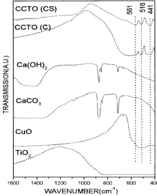
Figure 3 shows the IR spectra of the ceramics CCTO(CS) and CCTO(C) together with the spectra of the starting materials. One can notice that the CCTO phase presents resonance absorptions at 561, 516, and 441 cm⫺1 for CCTO(CS). Several authors have assigned [10] this region of absorptions with the titanium ion. These bands were associated to TiOO ⫽ 653–550 cm
⫺1 and
Ti
OOOTi⫽495– 436 cm ⫺1. Figure 1 Comparison of the XRD of the calcinated sample CCTO(C)
and calcinated⫹sintered sample (CCTOCS) with CCTO reference
Figure 2 Comparison of the Raman spectra of the calcinated sample CCTO(C) and calcinated⫹sintered sample CCTO(CS)
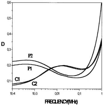
Figures 4 and 5 show the dielectric permittivity (K) of all the samples (C1 and C2 in Fig. 4 and P1 and P2 in Fig. 5) in the range of 100 Hz to 1 MHz. For all the samples, there is a decrease in the Kvalue for this range of frequency. For samples C1 and C2 at 100 Hz,K⬃1800 decreases to 800 at 1 MHz. For samples P1 and P2, where we did not use any organic binder, the dielectric constant was higher. For samples P1 and P2 at 100 Hz, K ⬃ 10.000 decreases to 4.000 at 1 MHz. We believe that the presence of the organic binder plays a critical role in its effect on the grain size and boundaries, which thus affects the effective dielectric constant of the ceramic [8]. Figure 6 depicts the dielectric loss for all the samples. At low frequencies, the P1 and P2 samples present higher
losses, as compared to the C1 and C2 samples. The loss increases with the frequency and is around 0.35 for samples C1 and C2 at around 1 Mz. Table 1 gives the dielectric constant and loss for all the samples at 1 KHz and 1 MHz.
The increase of the loss for all the samples with frequency has been reported in the literature [8].
To investigate the potential application of the CCTO materials for microwave planar devices, a series of planar microstrip anten-nas was made. The demand for new mobile communication sys-tems will lean heavily toward miniaturization and low-volume devices and equipment. Due to these requirements in portable or repeater stations in cellular systems for mobile communication for example, high dielectric constant materials can be used to effec-tively reduce the size of planar microstrip antennas [11].
The performance of a planar antenna is related to theLandW dimensions of the patch and the dielectric constant K of the substrate. For the best compromise among antenna gain, effi-ciency, bandwidth, and volume, an adequate material with a high Kmust be found for low volume. Of course, there is a tradeoff: high dielectric constant materials provide a low-volume antenna, but impose low bandwidth and gain. Moreover, there is a demand for monolithic integration of antennas and associated circuitry and these requirements claim compatible high dielectric constant ma-terials.
Simple rectangular antenna prototypes were designed on sub-strate samples nominally 3– 4 cm in diameter and 2–3 mm thick (see Table 1). The resonant frequency was calculated in the range of 2–3 GHz, based on the dielectric constant available data [1–3, 8]. One of the experimental antennas is shown in Figure 7 (sample C1).
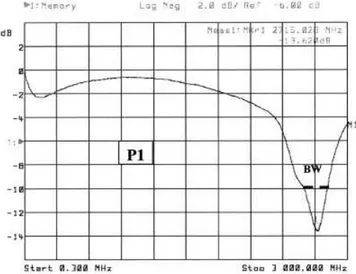
All the samples show the electromagnetic radiator’s potential properties, that is, antenna. This is proved when the dips in theS11 measurements reach values lower than⫺10 dB. The⫺10-dB point in the S11 parameter corresponds to a VSWR of 2:1. The S11 parameters (return loss) for the antennas were measured. The results are shown in Figure 8 for the P1 antenna. The VSWR⬍2:1 (⫺10-dB line) criterion, used to identify the antenna bandwidth and the dip in theS11measurement (see Fig. 8) below⫺10 dB, is Figure 4 Dielectric constantKof samples C1 and C2 in the frequency
range of 100 Hz to 1 MHz
Figure 5 Dielectric constantKof samples P1 and P2 in the frequency range of 100 Hz to 1 MHz
a preliminary indicator of the electromagnetic radiation properties of the device.
As a typical result, a 90-MHz BW was found for the antennas (with P2, C1, and C2 as substrates), which is lower than that of typical rectangular patch antennas with low dielectric constant substrates, of about 3%. The antenna with P1 substrate presented a surprisingly high BW of 270 MHz that corresponds to 10% bandwidth at 3 GHz. Such a value is in accordance with the requirements for planar antennas in a variety of wireless commu-nication systems, such as WLAN, PCS, Wi-Fi, and other protocols. Therefore, these measurements confirm the potential use of such materials for small planar high dielectric antennas (HDA).
In summary, the CCTO samples present higher DC for the samples prepared without any organic binder (K⫽7370 and 7073 for P1 and P2, respectively, at 1 KHz), as compared to the samples prepared with the organic phase (K⫽1641 and 1530 for C2 and C1, respectively, at 1 KHz); refer to Figures 4 and 5 and Table 1. The presence of the organic phase can be used to control the value of the DC and loss of the material. However, the loss is still a problem to be studied regarding applications in the microwave region.
The performance of a planar microstrip antenna that uses the CCTO ceramic as a high DC substrate was examined. Simple rectangular antenna prototypes were designed on substrate samples (C1, C2, P1, and P2; see Table 1). For the antennas (with P2, C1, and C2 as substrates), the BW is 90 MHz (around 3%). The antenna with P1 substrate presented a surprisingly high BW of 270 MHz that corresponds to a 10% bandwidth at 3 GHz. Such a value is in accordance with the requirements for planar antennas for a variety of wireless communication systems such as WLAN, PCS, Wi-Fi, and other protocols. Therefore, these measurements con-firm the potential use of such materials for small high-dielectric planar antennas (HDA).
These materials are also very promising for capacitor applica-tions and certainly for microelectronics and microwave devices (cellular mobile phones, for example), where miniaturization of the devices is critical.
4. CONCLUSION
In conclusion, a traditional ceramic (solid-state) procedure was used to produce bulk ceramics of CCTO (CaCu3Ti4O12). The samples of the CCTO ceramic were studied by X-ray powder diffraction, and infrared and Raman scattering spectroscopy. After 30 h of milling, the formation of CCTO was confirmed by X-ray powder diffraction. The infrared and Raman scattering
spectros-copy confirmed the formation of the CCTO phase as seen by XRD analysis. The first experimental procedure used an organic binder in the process of shaping the samples. In the second procedure, the samples were prepared without the presence of the organic phase, and we obtained a higher dielectric constant (K ⫽ 7370) with high loss (D ⫽ 0.2) at 1 KHz. For the first procedure, a lower dielectric constant (K ⫽1530) and lower loss (D ⫽0.11) at 1 KHz were obtained. Simple rectangular antenna prototypes were also designed on substrate samples (C1, C2, P1, and P2). For the antennas (with P2, C1, and C2 as substrates), the BW was 90 MHz (around 3%). The antenna with P1 substrate presented a surpris-ingly high BW of 270 MHz, which corresponds to a 10% band-width at 3 GHz. Such a value is in accordance with the require-ments for planar antennas in a variety of wireless communication systems, such as WLAN, PCS, Wi-Fi, and other protocols. There-fore, these measurements confirm the potential use of such mate-rials for small planar antennas. These matemate-rials are attractive for capacitor applications, as well as for microelectronics and micro-wave devices (cellular mobile phones, for example), where min-iaturization of the devices is crucial.
ACKNOWLEDGMENTS
This work was partly sponsored by Ericsson EDB, Ericsson Re-search Center Brazil, under contracts Ericsson/UFC-06 and UNI.15/00 and by FINEP, CNPq, CAPES (Brazilian agencies). We also thank A. G. Souza Filho for the Raman measurements.
REFERENCES
1. M.A. Subramanian, D. Li, N. Duran, B.A. Reisner, and A.W. Sleight, J Solid State Chem 151 (2000), 323–325.
2. A.P. Ramirez, M.A. Subramanian, M. Gardel, G. Blumberg, D. Li, T. Vogt, and S.M. Shapiro, Solid State Commun 115 (2000), 217. 3. M.A. Subramanian and A.W. Sleight, Solid State Sci 4 (2002), 347. 4. N. Setter and E.L. Colla, Ferroelectric ceramics, Birkhauser Verlag,
1993.
5. B. Bochu, M.N. Deschizeaux, and J.C. Joubert, J Solid State Chem 29 (1979), 291.
6. A.F.L. Almeida, R.S. de Oliveira, J.C. Go´es, J.M. Sasaki, J. Mendes Filho, and A.S.B. Sombra, Mat Sci and Eng B 96 (2002), 275–283. 7. R.S. de Figueiredo, A. Messai, A.C. Hernandes, and A.S.B. Sombra, J
Mat Sci Lett 17 (1998), 449.
8. P. Jha, P. Arora, and A.K. Ganguli, Mat Lett 4179 (2002), 1– 4. Figure 7 Planar microstrip antenna on CCTO substrate for 3-GHz
op-eration
9. N. Kolev, R.P. Bontchev, A.J. Jacobson, V.N. Popov, V.G. Hadjiev, A.P. Litvinchuk, and M.N. Iliev, Phys Rev B 66 (2002), 132102. 10. S. Music, M. Gotic, M. Ivanda, S. Popovic, A. Turkovic, R. Trojko, A.
Sekulic, and K. Furic, Mat Sci and Eng B 47 (1997), 33.
11. B. Lee and F.J. Harackiewicz, IEEE Trans Antennas Propagat 50 (2002), 1160.
© 2003 Wiley Periodicals, Inc.
A NEW COMPACT 1D PBG
MICROSTRIP STRUCTURE WITH
WIDER STOPBAND BASED ON
SEMICONDUCTOR SUBSTRATE
Wenmei Zhang,1,2Xiaowei Sun,2Junfa Mao,1Rong Qian,2
and Dan Zhang2
1Department of Electronic Engineering
Shanghai Jiao Tong University Shanghai, 200030, P. R. China
2Shanghai Institute of Micro-system and Information Technology
Chinese Academy of Sciences Shanghai, 200050, P. R. China
Received 26 March 2003
ABSTRACT:A new type of compact one dimensional (1D) micro-strip photonic bandgap (PBG) used for filters is presented. A semi-conductor-based structure of a miniature band-stop filter with three cells is simulated, realized, and measured. Basic agreement between the experimental and simulated results have been achieved. The filter with the proposed PBG structure exhibits wide, deep, and steep stop-band characteristics, and also has less loss and ripples in the pass-band. Thus, the new PBG structure can be used for low-pass as well as high-pass filters. The period of the PBG lattice is about (1/5⬃
1/4)e(eis the guiding wavelength at the center frequency of the stop-band), or 0.080(0is the wavelength in air). The filter with the new PBG structure is much easier to fabricate and integrate with other circuits and is more compact than conventional filters. The re-sults in our paper are based on semiconductor substrate and can be applied directly in MIC and MMIC.© 2003 Wiley Periodicals, Inc. Microwave Opt Technol Lett 39: 150 –152, 2003; Published online in Wiley InterScience (www.interscience.wiley.com). DOI 10.1002/mop. 11153
Key words:microstrip; photonic bandgap (PBG); bandstop filter; low-pass filter; high-low-pass filter; slow wave
1. INTRODUCTION
The idea of employing photonic bandgap (PBG) was first proposed by Yabnolovitch in 1987 [1]. A PBG device is a periodic structure in which electromagnetic waves in a certain frequency band cannot propagate or be strongly attenuated. Therefore, it has been used largely for electromagnetic wave propagation control. Also, a PBG device is slow-wave structure. When it was introduced, the size of devices can be reduced.
Several papers have focused on achieving compact design and wider frequency stopband. For example, Kelly [2] proposed a serial connection of several different PBG structures for wide-rejection-frequency bandwidth, but this required large size and had limitations for microstrip-circuit applications of compact size. In [3], the proposed structure was connected in parallel with two periodic structures that have different center frequencies of the stopband. In [4], a novel multiplayer structure was used to enhance the width of the stopband. The abovementioned filters have etching in the ground plane. A disadvantage of this structure is packaging
problem and realization of MMICs: the etched ground plane must be sufficiently far from any metal plate in order to maintain the etched patterns’ function. Also, the position of the signal line in reference to the etched ground plane has an influence on the final characteristics. So, Nesic proposed a novel PBG microstrip struc-ture without etching in the ground plane as a filter [5], which is also a low-pass filter.
In this paper, a new compact microstrip PBG structure for filters is proposed. The filters adopting the proposed PBG structure exhibit wide, deep, and steep stop-band characteristics, and also have small and few ripples at the higher pass-band. So it can also be used in high pass filters. The period of the PBG lattice is about (1/5 ⬃ 1/4) e. The simulation was done using Agilent ADS software.
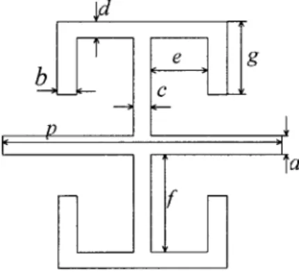
2. DESIGN OF THE NEW 1D MICROSTRIP PBG CELL The proposed 1D microstrip PBG cell is shown in Figure 1. Inductance corresponds to the narrow lines, and capacitance cor-responds to the gap between the narrow lines (Fig. 1). The addi-tional capacitance and inductance determine the propagation con-stant, which is much larger than that of a conventional microstrip line. The achieved slow-wave can be used to reduce the size of filter. By tuning the length of every line and the gap between the lines, different slow-wave effects can be attained at different frequency. For simple design,a⫽ b⫽ c⫽ dis assumed. 3. MEASUREMENT RESULTS
According to the characteristic of the proposed PBG structure, a filter with wider stopband for a system is designed. The signal of the system comes from the oscillatory working at 16.5 GHz. This filter was originally developed to meet the following specifications for a system application.
Min. stop-band rejection: 16.5 GHz ⫺20 dB 33 GHz ⫺10 dB Insertion loss: 36 GHz ⫺2 dB
The realized filter is shown in Figure 2. The substrate used is gallium-arsenide with a dielectric constant of 12.6 and thickness of 0.25 mm. TheSparameter was measured with an HP 8722D net analyzer and a Casecade probe station. The simulated and mea-suredSparameters fora⫽ b⫽ c⫽ d⫽ 0.09 mm,e ⫽0.14 mm,f⫽0.53 mm,g⫽0.44 mm, andp⫽0.94 mm are shown in Figure 3. The phase responses of the realized structure (includ-ing the 50⍀microstrip line for connectors) and a 50⍀microstrip line of the same length are presented in Figure 4. In Figure 3, basic agreement between the experimental and simulated results has