Erbium in a-Si:H
Leandro R. Tessler
Instituto de Fsica \Gleb Wataghin", UNICAMP, C. P. 6165, 13083-970, Campinas, SP, Brazil
Received 27 May, 1999
A review of the current status of research on Er3+doped hydrogenated amorphous silicon (a-Si:H)
is presented. Er has been introduced in a-Si:H and a-SiOx:H by ion implantation, co-sputtering and
PECVD. In all cases, the characteristic atomic-like intra-4f 4
I
13=2 !
4
I
15=2 photoluminescence
emission ats1.54m is observed at room temperature. The Er
3+luminescence probability is
de-termined by the local neighborhood of the ions. Therefore, local probes like EXAFS and Mossbauer spectroscopy have yielded very important information. A discussion of excitation processes, elec-troluminescence, and electronic doping eects, is also presented.
PACS Number(s): 71.23.Cq, 73.61.Jc, 81.05.Gc
I Introduction
The global telecommunications network has experi-enced an enormous expansion in the last few years. The present bandwidth requirements are beyond the capability of conventional electronic technology. One solution for this problem has been the development of photonics, the use of light for information processing and distribution. Silica-based ber optics have allowed a bandwidth increase of orders of magnitude relative to microwaves or cabled communications. Commercial systems are already irting with the terabit/sec bar-rier on a single ber[1]. In the laboratory, 2.6 Tbit/sec has been achieved over 120 km of ber[2]. Conven-tional silica optical bers present the minimum atten-uation losses at wavelengths near 1.5m, dening the
so-called \third spectral window" (the other two are respectively at 0.9 and 1.3 m) An important
chal-lenge to materials and semiconductors scientists nowa-days is to develop light sources and detectors operat-ing at these wavelengths at low cost and high relia-bility. Moreover, it would be advantageous if the new devices would be compatible with the well established silicon microelectronic technology. Currently the only reliable light sources for ber optics are the III-V near-band edge lasers, whose high cost render large scale consumer applications prohibitive. An important al-ternative consists on the use of rare-earth based light emitters, which operate based on the atomic-like
tran-sitions within the incomplete 4f levels of these
ele-ments. A great eort has been devoted to the study of rare-earth doped semiconductors[3, 4], specially er-bium doped silicon that emits light in the third spectral window range. The recent developments are inducing the emergence of a new eld of research, that of silicon-based optoelectronics[5].
The rare earth elements are distinguished by their incomplete internal 4f shell. When diluted in solid
hosts, the rare earth atoms become almost always triva-lent ions, losing the two 6sand one 4f electrons. The
4felectrons are shielded from external elds by the two
remaining electronic shells with larger radial extension (5s
25 p
6). The intra 4
f electronic transitions are thus
atomic-like, weakly dependent on the details of the lo-cal chemistry. However, f ,f transitions are electric
dipole forbidden (l= 0) in free ions. Only when the
rare earth ions are incorporated in a solid host which breaks inversion symmetry and mixes states of opposite parity is the transition allowed. The transition proba-bility is, therefore, strongly dependent on the chemical neighborhood of the ions. Among the rare earths, Er3+
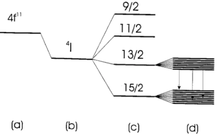
has been the most widely studied because the transi-tion between its two lowest spin-orbit levels corre-sponds to the emission of a photons with wavelengths close to 1.54m[6]. The local eld splits the spin-orbit
manifolds into a number of Stark levels. The degener-acy g of each state is given by g =J + 1=2, so there
broadened both homogeneously or inhomogeneously[7]. A schematic representation of the level distribution of Er3+ is found in Figure I.
Figure 1. Schematic representation of (a) the 4f
11 states.
(b) Electron-electron interaction. (c) Spin-orbit interaction. (d) Stark splitting. Some possible luminescent transitions are indicated.
In this paper I review the current status of Er doping of amorphous silicon, with emphasis in co-deposition techniques. Although the main subject is infra-red photoluminescence, other electronic as well as relevant structural properties are also covered.
II Preparation of Er doped
a-Si:H
A. Ion Implantation
Ion implantation has been used extensively as a means to incorporate Er in solids. Excellent re-view papers concerning erbium ion implantation for photonics[8] and about erbium ion implantation in silicon[9] are available. Er implantation in unhydro-genated a-Si[10] provided weak photoluminescence, de-tectable only at low temperatures. Er implantation on PECVD[11] or sputtered[12] samples, however, pro-vided samples with room temperature photolumines-cence after annealing at 300-850 C. The
lumines-cence intensity was increased a factor 2 by oxygen co-implantation. Ion implantation in amorphous SIPOS (Semi-Insulating Poly Silicon, a silicon alloy containing up to 30 at.% O and H) yielded samples with higher lu-minescence intensity and lower temperature quenching than crystalline silicon[13]. Ion implantation is a well established technique, which provides good control of the concentration prole in the sample, an yielded the best electroluminescent devices to date in crystalline
silicon[14]. However, because of the unavoidable dam-age associated with the implantation process, a high temperature annealing step is imperative. It is well known that annealing a-Si:H aboves400
C causes
hy-drogen eusion, which deteriorate the electronic prop-erties of a-Si:H.
B. Co-deposition
In order to avoid the implantation damage due to ion implant, co-deposition techniques were developed by some research groups. These techniques can be roughly divided in variations around sputtering and PECVD, which are the most widely used processes for the preparation of electronic quality a-Si:H.
Sputtering
Sputtering is a deposition technique in which a-Si:H is formed from Si atoms removed from a Si target by momentumtransfer from a cold plasma, normallyof Ar. Molecular hydrogen is added to the sputtering gas to passivate the Si dangling bonds. The rst report[15] of Er3+ luminescence from co-deposited a-Si:H
hEri used
rf-sputtering for sample preparation. Two targets, one of pure Si and one of pure Er were interchanged in the cathode during the deposition process, alternating 60 sec Si cycles with 5-10 sec Er cycles. The samples obtained presented a-Si:H photoluminescence at low temperatures and also Er3+ luminescence which was
stronger than that from an Er3+ doped crystalline Si
sample. Adding Yb3+ to a-Si:H using the same
depo-sition technique did not result in Yb3+ luminescence.
Erbium photoluminescence (PL) in a-Si:H with much less temperature quenching was obtained in as-deposited samples by using the MASD[16], a modied sputtering technique. In this process[17], a metallic Er target is put in a dc-magnetron sputtering congura-tion, and the sputtering gas consists of an Ar+SiH4
mixture.
More recently another possibility has been explored: rf-sputtering deposition from a Si substrate partially covered by small metallic Er platelets[18]. Using this procedure it is possible to control the Er concentra-tion in the sample over a wide range. As-deposited samples present room-temperature Er3+ PL, although
thermal annealing increases the PL eciency. The de-position conditions that yield the strongest Er3+ PL
be added to the material during deposition. This is eas-ily done by adding a controlled leak to the deposition chamber[19, 20] and resulted in samples with optimized as-deposited room temperature PL.
PECVD
The best electronic quality a-Si:H lms, adopted by the solar cell and TFT industry, are prepared using the PECVD technique. This has motivated studies of the preparation of a-Si:HhEriby this process. In this
tech-nique a-Si:H is formed from plasma decomposition of silane (SiH4), in a much smoother process than
sput-tering. The resulting lms have a density of states in the gap that can be one order of magnitude be-low that of comparable lms obtained by sputtering. The main problem is the need of a suitable carrier to bring Er to the deposition chamber. The carrier gases are normally metalorganics, and the carbon contami-nation of the samples is unavoidable. Recently, the St. Petersburg group has been able to prepare Er doped a-Si:H by PECVD, using either Er(HFA)3
DME[21] or
Er(TMHD)3[22]. The latter found vibration modes in
the infra-red absorption spectrum that were associated with carbon.
III Structural Properties
Composition
Sample composition is often measured by Ruther-ford Backscattering Spectroscopy (RBS), which is a very appropriate technique for quantitative measure-ments of heavy impurities concentrations in light hosts. One important result, which is frequently disregarded is the presence of residual oxygen in a-Si:H, in concen-trations in the 0.2 to 0.3 at. % range [16, 11, 19]. This residual oxygen plays a very importantrole in determin-ing the electronic properties of the material. Moreover, the presence of small oxygen partial pressures during co-sputtering inhibits the deposition rate of Er, most probably because of the high reactivity between these two elements.
Local Properties
Since the 4 I
13=2 !
4
I
15=2 transition probability is
determined by the local environment of the Er3+ ions,
the information about their chemical neighborhood is very important. Two local techniques have been used
to study Er in a-Si:H: Mossbauer spectroscopy and EX-AFS.
MossbauerSp ectroscopy
Mossbauer spectroscopy studies[23, 24] were per-formed in a-Si:HhErisamples prepared using the MASD
technique[16]. The samples were irradiated with slow neutrons to become rich in 169Er and 169Er(169Tm)
emission Mossbauer spectra were recorded. The results reveal the superposition of a singlet and a quadrupole doublet. The singlet is attributed to a silicon coordi-nation shell and the quadrupole to a non-cubic oxy-gen neighborhood. In samples exhibiting Er3+ PL, the
quadrupole signal is maximum, indicating that the op-tically active Er3+ is arranged within Er-O clusters.
EXAFS
EXAFS is a very useful technique to determine the coordination of Er in silicon. It was used to establish that in crystalline silicon luminescent Er3+ is
coordi-nated with oxygen as in Er2O3[25]. In a-Si:H the
situa-tion is similar but the Er neighborhood has important dierences[26]. It was shown[27] that in co-sputtered samples the rst neighbor shell consists of oxygen atoms with an average coordination between 2 and 3.6, com-pared to 6 in Er2O3. Furthermore, the average Er-O
separation is much smaller (up to 0.2 A) than in Er2O3
and is minimum for an average coordination of 3. The results indicate that ErO3clusters are the energetically
favored conguration of Er in a-Si:H. Being a strong oxygen getter, Er tends to be bonded to all the avail-able residual O during deposition, and is incorporated to the a-Si:H network in the form of ErOx clusters.
IV Electronic Properties
Photoluminescence
Infra Red
Most of the studies of a-Si:HhEri have as ultimate
goal the optimization of the photoluminescence inten-sity at room temperature. The Er3+
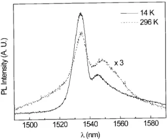
photolumines-cence spectrum in a-Si:H consists of a characteristic double peak structure (Fig.2), which at room tem-perature is very similar to Er3+ in crystalline silicon.
wavelength one. No additional structure can be re-solved down to 2 K [28]. The spectral width of the main peak and the wide tails are due to Stark split-ting of the excited and ground states, by the local elec-tric eld, which can be broadened homogeneously or inhomogeneously[7]. The exact position of the peaks depend on the oxygen content of the sample[11] and very weakly on the temperature [19]. The PL inten-sity depends on the oxygen content, and an optimum is found at around 10 oxygen atoms per erbium[19, 20]. This is probably related to the formation of ErO3
clusters[27], the remainder oxygen being bonded to sil-icon. The temperature dependence of the luminescence intensity is represented in Figure IV. The temperature quenching optimized samples between 20 and 300K[19], slightly greater than a factor 3, is much smaller than in crystalline or in ion implanted amorphous silicon[8]. This quenching is much stronger above 70K.
Figure 2. Typical Er3+ in a-Si:H photoluminescence
spec-tra. The temperatures are indicated.
One important property of a-Si:HhEri is the
ex-istence of an ecient process of excitation transfer from the host to the ions. Photoluminescence excita-tion curves[29] show that the PL intensity closely fol-lows the absorption coecient of a-Si:H. This is very important for electroluminescent devices applications. In glasses[30], the resonant excitation process is much more ecient than excitation transfer.
The whole photoluminescence process is then (i) absorption of a photon by the host, generating an electron-hole pair, (ii) transfer of the excitation to an Er3+ ion, (iii) radiative decay of the ion.
The 4f states are 10-20 eV below the valence states
of a-Si:H. Two processes have been proposed for the
ex-citation of rare earth impurities in semiconductors[31]: impact and Auger excitation, the probability of the latter increasing in the presence of localized states. Indeed, a Defect Related Auger Excitation (DRAE) mechanism[29, 32] in which Er ions are Auger excited with the capture of band-tail electrons by neutral de-fects is consistent with experimental results, in partic-ular with the temperature quenching curves.
During any of the steps (i), (ii) or (iii) non-radiative loss of the excitation may occur. The recombination of an electron-hole pair in a defect not resulting in Auger excitation may take place during step (i). This is the reason why the PL intensity decreases if the samples are annealed at temperatures above 400C. Above this
temperature, the intensity of infrared absorption by the Si-H vibration mode ats650 cm
,1decreases[28, 33],
in-dicating out-diusion of hydrogen, which increases the density of dangling bonds.
There are controversial opinions concerning the main cause of temperature quenching of the PL. In implanted samples the quenching has been explained supposing an increase of the backtransfer rate of the excitation[11] (step iii), while in MASD samples it has been attributed to the decrease of the excitation rate [29] (step ii). Our own data[19] of PL intensity de-pendence on the laser intensity over 2 decades for co-sputtered samples seems to support [29]. More studies are necessary to clear this point. It is our belief that the quenching mechanism should not depend on the form of sample preparation.
Figure 3. Temperature quenching of the Er3+luminescence
Visible
If the gap of the host is high enough, it is possi-ble to observe transitions between higher excited states of Er3+[34, 35]. This was achieved by adding as much
as 10 at. % Er to unhydrogenated a-SiN, with a high gap. Green luminescence (s545 nm) was detected at
room temperature corresponding to the4 S
3=2 !
4
I
15=2
transition. Notice, however, that in this material the PL eciency is probably small and unlike the case of a-Si:HhEri, strong resonance excitation eects are
ob-served, indicating that excitation transfer from the host is rather inecient. Nevertheless, these results widen the range of potential applications of rare earth doped amorphous silicon based alloys.
Electroluminescence
Er3+ electroluminescence (EL) has been achieved
in a-Si:HhEri. A simple heterojunction diode
congu-rationn-type Cz-Si/a-Si:HhEri/Al emits EL at 1.54m
when reverse biased in the breakdown region[32]. Crys-talline silicon is transparent at this wavelength and EL can be detected from the substrate side. Under direct bias holes are injected in the a-Si:HhEri layer,
trans-verse it and recombine radiatively at the crystalline sub-strate emitting near-band gap 1.2m luminescence. No
Er3+ luminescence is observed under direct bias. This
result was reproduced in our laboratory, albeit our de-vices presented lower breakdown voltages[19]. No EL signal was detected at reverse bias voltages below the onset onset of breakdown, indicating that impact pro-cesses may be at least partially responsible for the exci-tation. The electric eld and temperature dependence can be explained by the DRAE model[36]. The perfor-mance of these devices is quite poor, and more research is necessary before ecient devices can be developed.
Doping Eects
Doping of amorphous semiconductors is generally achieved by adding impurities of groups III or V of the periodic table. However, the addition of rare earth ions may have doping eects in a-Si:H in the sense of con-trolling the electronic properties of the material and determining the Fermi level position. From electrical equilibrium considerations, it would be expected that under a charge transfer doping mechanism Er3+ would
be a donor in silicon. Early reports on crystalline silicon indicated p-type doping[37], while more recent results
have found the expected n-type doping[38, 39]. In
un-hydrogenated a-Si, several dierent rare earths turned
out to be acceptors and p-type doping was found[40].
In a recent work, Er3+ doping eects were measured
in a-Si:H and this doping was classied as n-type,
al-though no measurements were made to determine the majority carriers[29]. Thermopower measurements at room temperature[27] indicated p-type character. The
question raised is why Er3+ is sometimes a donor and
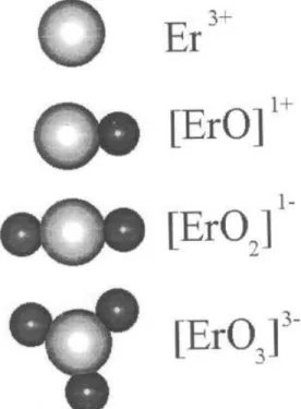
sometimes an acceptor. In fact this behavior results from the peculiar chemistry of Er[27]. Being a strong oxygen getter, Er is incorporated to the network in the form of [ErO]
+3,2 complexes, the most stable
con-guration being for = 3, as represented in Figure
IV. For an average <1:5 the complexes have donor
behavior, whilst for an average>1:5 they are
accep-tors. In a-Si:H, the usual Er concentrations and resid-ual O content are such that >2 and p-type doping
results. Systematic doping studies with controlled oxy-gen concentration are needed to test this model. Charge transfer doping of amorphous semiconductors is a new subject of study.
Figure 4. Schematic model of Er-O clusters that are formed in a-Si:H.
V Conclusions
The study of a-Si:HhEriis rapidly becoming an
In this paper I reviewed relevant issues like preparation methods, structural and electronic properties, with em-phasis in photoluminescence. Although the community has reached some degree of understanding, some funda-mental topics remain open: What process determines the temperature quenching? What is the doping mech-anism? Can higher photoluminescence and electrolumi-nescence eciencies be achieved? What is the exact role of oxygen? What can be expected from dierent amorphous semiconductor hosts? And from dierent rare earth dopants? And from dierent co-dopants?
There are apparently more open questions than an-swers. That is why I believe this is and will be a very exciting eld of research in the years to come.
Acknowledgements
It is a pleasure to acknowledge all collaborators who actively participated in the activities concerning the a-Si:HhEri project: A. C. I~niguez, C. Piamonteze and
E. Horta, at UNICAMP, M. C. Martins Alves and H. Tolentino at LNLS, and A. R. Zanatta now at USP-S~ao Carlos. M. Tabacniks from USP-USP-S~ao Paulo always helped us with the RBS measurements. Continuing support from my colleagues at the Laboratory of Photo-voltaic Research and at GFURCO, UNICAMP is grate-fully acknowledged. The discussions with I. Solomon at the very early stages of the project were very illuminat-ing. This work would not have been possible without the nancial support of CNPq, FAPESP and PRONEX \Fot^onica em Telecomunicac~oes".
References
[1] G. Styx, Scientic American, December 1998, pp. 9-10. [2] G. P. Agrawal, Fiber-Optic Communication Systems,
2ndedition, (John Willey, New York, 1997) p. 287.
[3] Rare Earth Doped Semiconductors, edited by G. S. Pomrenke, P. B. Klein and D. W. Langer, (MRS Symp. Proc.301, Pittsburgh, 1993).
[4] Rare Earth Doped Semiconductors II, edited by A. Pol-man, S. Coa, and R. Schwartz, (MRS Symp. Proc.
422, Pittsburgh, 1996).
[5] Silicon-baseoptoelectronics,MRS Bulletin23(4), April
1998.
[6] S. Hufner, Optical Spectra of Transparent Rare Earth Compounds, (Academic Press, New York, 1978). [7] E. Desurvire, Erbium Doped Fiber Ampliers, (John
Wiley, New York, 1994).
[8] A. Polman, J. Appl. Phys.82,1 (1997).
[9] S. Coa, S. Lombardo, F. Priolo, G. Franzo, S. U. Campisano, A. Polman and G. N. van den Hoven, Il Nuovo Cimento18D, 1131 (1996).
[10] J. S. Custer, E. Snoeks and A. Polman, inPhase For-mation and Modication by Beam-Solid Interactions, edited by G. S. Was, L. E. Rehn and D. Follstaed, (MRS Symp. Proc235, Pittsburgh, 1992) p. 51.
[11] J. H. Shin, R. Serna, G. N. van den Hoven, A. Polman, W. G. J. H. M. van Sark and A. M. Vredenberg, Appl. Phys. Lett.68, 997 (1996).
[12] M. Kechouane, N. Beldi, T. Mohammed-Brahim, H. L'Haridon, M. Salvi, M. Gauneau and P. N. Favennec, inRare Earth Doped Semiconductors, (ref. [3]), p. 133. [13] G. N. van den Hoven, J. H. Shin, A. Polman, S. Lom-bardo and S. U. Campisano, J. Appl. Phys. 78, 2642
(1995).
[14] G. Franzo, S. Coa, F. Priolo and C. Spinella, J. Appl. Phys.81, 2784 (1997).
[15] T. Oestereich, C. Swialtowski and I. Broser, Appl. Phys. Lett.56,446 (1990).
[16] M. S. Bresler, O. B. Gusev, V. Kh. Kudoyarova, A. N. Kuznetsov, P. E. Pak, E. I. Terukov, I. N. Yassievich, B. P. Zakharchenya, W. Fuhs and A. Sturm, Appl. Phys. Lett.67,3599 (1995).
[17] V. Marakhonov, N. Rogachev, J. Ishkalov, J. Marakhonov, E. Terukov and V. Chelnokov, J. Non-Cryst. Sol.137&138, 817 (1991).
[18] A. R. Zanatta, L. A. O. Nunes and L. R. Tessler, Appl. Phys. Lett.70,511 (1997).
[19] L. R. Tessler and A. C. I~niguez, inAmorphous Silicon Technology -1998, (MRS Symp. Proc.507, Pittsburgh,
PA 1998), in press.
[20] V. Kh. Kudoyarova, A. N. Kuznetsov, E. I. Terukov, O. B. Gusev, Yu. A. Kudriavtsev, B. Ya. Ber, G. M. Gusinskii, W. Fuhs, G. Weiser and H. Kuehne, Semi-conductors 32, 1234 (1998) [Fiz. Tekh. Poluprovodn. 32, 1384 (1998)].
[21] V. B. Voronkov, V. G. Golubev, A. V. Medvedev, A. B. Pevtsov, N. A. Feoktisov, N. I. Gorshkov and D. N. Suglobov, Phys. Sol Stat.40,1301 (1998) [Fiz. Tverd.
Tela (St. Petersburg)40, 1433 (1998)].
[22] E. I. Terukov, O. I. Kon'kov, V. Kh. Kudoyarova, O. B. Gusev and G. Weiser, Semiconductors 32, 884 (1998)
[Fiz. Tekh. Poluprovodn.32, 987 (1998)].
[23] V. F. Masterov, F. S. Nasredinov, P. P. Seregin, V. Kh. Kudoyarova, A. N. Kuznetsov and E. I. Terukov, Appl. Phys. Lett.72,728 (1998).
[24] V. F. Masterov, F. S. Nasredinov, P. P. Seregin, E. I. Terukov and M. M. Mezdrogina, Semiconductors 32,
636 (1998) [Fiz. Tekh. Poluprovodn.32, 708 (1998)].
[25] D. L. Adler, D. C. Jacobson, D. J. Eaglesham, M. A. Marcus, J. L. Benton, J. M. Poate, and P. H. Citrin, Appl. Phys. Lett.61, 2181 (1992).
[27] C. Piamonteze, A. C. I~niguez, L. R. Tessler, M. C. Mar-tins Alves and H. Tolentino, Phys. Rev. Lett.81, 4652
(1998).
[28] L. R. Tessler and A. R. Zanatta, J. Non-Cryst. Sol.
227-230,399 (1998).
[29] W. Fuhs, I. Ulber, G. Weiser, M. S. Bresler, O. B. Gusev, A. N. Kuznetsov, V. Kh. Kudoyarova, E. I. Terukov and I. N. Yassievich, Phys. Rev. B56, 9545
(1998).
[30] W. J. Miniscalco, J. Lightwave. Tech.,9, 234 (1991).
[31] I. N. Yassievich and L. C. Kimerlingh, Semicond. Sci. and Technol.8, 718 (1993).
[32] O. B. Gusev, A. N. Kuznetsov, E. I. Terukov, M. S. Bresler, V. Kh. Kudoyarova, I. N. Yassievich, B. P. Za-kharchenya and W. Fuhs, Appl. Phys. Lett. 70, 240
(1997).
[33] A. R. Zanatta and L. A. O. Nunes, Appl. Phys. Lett.
71, 3679 (1997).
[34] A. R. Zanatta and L. A. O. Nunes, Appl. Phys. Lett.
72, 3127 (1998).
[35] A.R. Zanatta, M.J.V. Bell and L.A.O. Nunes, Phys. Rev. B (in press).
[36] O. Gusev, M. Bresler, A. Kuznetsov, V. Kudoyarova, P. Pak, E. Terukov, K. Tsendin, I. Yassievich, W. Fuhs and G. Weiser, J. Non-Cryst. Sol.227-230,1164
(1998).
[37] H. Ennen, G. Pomrenke, A. Axman, K. Eisele, W. Haidl and J. Schneider, Appl. Phys. Lett. 46, 381
(1985).
[38] J. L. Benton, J. Michel, L. C. Kimerling, D. C. Jacob-son, Y. -H. Xie, D. J. Eaglesham, E. A. Fitzgerald and J. M. Poate, J. Appl. Phys.70, 2667 (1991).
[39] S. Libertino, S. Coa, G. Franzo and F. Priolo, J. Appl. Phys.78, 3867 (1995).