Abstract— In this paper, an in-depth study of the electrical and optical characteristics of Polymer Light Emitting Diodes ITO/PEDOT: PSS/DP-PPV derivatives/Al(Ca) is presented. Three polymer materials are considered; poly(2,3-diphenyl-5-(4 -heptyloxy-4’-oxytrimethylenediphenyl)-phenylenevinylene) (P1), poly(2,3-diphenyl-5-[4-(4-pentylcyclohexyl)phenoxy]-propyl-p -phenylene vinylene) (P2) and poly(2,3-diphenyl-5-(2-(1, 4, 5 -triphenyl-1H-2-imidazoloyl)-1-oxytrimethylene phenyl) phenylene vinylene) (P3). The J-V characteristics are investigated using a device model which includes the injection, transport, and recombination mechanisms. The electron and hole mobility of each material are fitted to experimental data. The charge balance factor CBF, the external quantum efficiency EQE, the Langevin recombination rates and the singlet exciton densities profiles are studied. The results are found to be in a good agreement with experimental data especially in the low current densities region, indicating that these PLEDs electrons mobility affects greatly the J -V characteristics compared with holes mobility, and that is because electrons band offset smaller than that of holes. The best performance is obtained with P1 device with a CBF value of almost unity and an EQE still low (4.7 %) but similar to other PPVs and MEH-PPVs based devices.
Index Terms— Electrical and optical properties, Finite difference modeling, Organic light emitting diode.
I. INTRODUCTION
The rapid evolution of Organic Light Emitting Diode “OLEDs” gave rise to the exploration and
development of Organic Semiconductors ''OSCs'' fields; Organic Field Effect Transistors OFETs,
Sensors and solar cells [1]-[6]. OLEDs flat panel display is the next generation technology for a wide
variety of applications such as TV’s and handheld displays like smart phones, tablet computers and
cameras. Since the discovery of conjugated polymers [7] and the manufacturing of the first organic
light emitting diode [8] with its unique properties (better power efficiency, fast response time, wide
viewing angle, flexible and light weight substrates), extensive researches were made to understand and
to improve these devices efficiency i.e. the injection, transport, recombination mechanisms . OLEDs
structures were developed in the beginning by using polymers to study mainly single layers LEDs
known by PLEDs [9]-[15] then polymers and small molecules for complex structures (bilayer and
multilayer OLEDs).In order to improve their performance, phosphorescent and fluorescent materials
Electrical and optical numerical modeling of
DP
-
PPV based polymer light emitting diode
K. Benatia and A. Telia
Instrumentation and Microsystems Laboratory (LMI), Constantine 1 University, route Ein El Bey, Constantine 25000, Algeria
[16], [17] or graphene [18], [19] instead of the conventional Indium Tin oxide (ITO) were used.
Furthermore, many advanced materials were explored in the manufacturing and studying OLEDs on
the nanoscale like the quantum dots [20], carbon nanotubes [21] and nanowires [22].
Even though OLEDs technological breakthrough, single layer light emitting diodes based on
polymers are still of great interest and several methods were used to understand their devices physics
[23]- [25]. Enhanced by the discovery of semiconducting polymers, the PPV [Poly (Phenylene
Vinylene)] and the MEH-PPV Poly [2-Methoxy, 5-(2'-Ethyl-Hexyloxy)–1, 4-PhenyleneVinylene]
were intensively studied 9-15) more than any other PPVs derivatives material.
For several years, great effort has been devoted to the study of another PPVs derivative because of
its interesting properties, which is the Poly (2, 3-Diphenyl-1, 4-Phenylene Vinylene) (DP-PPV)
[26]-[34]. Many scientists working on this material were mostly focused on the design and synthesis routes
for highly efficient PLEDs, by characterizing the topographies of the DP-PPV based device surfaces
[26], attaching phenyl groups to PPV to obtain a fully conjugated polymer [27] or investigating the
influence of the materials structure on its properties [28]. Through these chemical modifications,
better results were achieved: higher electroluminescence efficiencies [26], solubility improvement,
efficient and highly thermal luminescence, high photoluminescence efficiency (while preserving the
energy gaps of the parent polymer) [27] and a super high brightness and an efficient luminance [29].
The tremendous progress done by these scientists [30] - [34] was our starting point for studying the
device physics of the DP-PPV. This is the first study to undertake a longitudinal analysis of DP-PPV
based devices properties. We propose, therefore, a new approach to this field of research by exploring
the electrical and optical characteristics of these polymer based devices, through a numerical model of
a bipolar single layer OLED with undoped organic layer trap free. The Ref. 30 synthesized three
substituted DP-PPV derivatives as shown in Figure 1: poly(2,3-diphenyl-5-(4-heptyloxy-4’
-oxytrimethylenediphenyl)-phenylene vinylene) (P1),
poly(2,3-diphenyl-5-[4-(4-pentylcyclohexyl)phenoxy]-propyl-p-phenylene vinylene) (P2) and poly(2,3-diphenyl-(2-(1, 4,
5-triphenyl-1H-2-imidazoloyl)-1-oxytrimethylene phenyl) phenylene vinylene) (P3), the J-V
characteristics, luminance, electroluminescence and photoluminescence were presented. Nevertheless,
there are still some interesting and relevant characteristics to be addressed. Electrical and optical
characteristics are studied: the influence of the injection barriers and carriers transport on current
density, Charge Balance Factor “CBF”, recombination power efficiency “CBFp”, External Quantum Efficiency “EQE” , recombination rate and singlet excitons density.
The paper is organized as follows: section 2 and 3 describe the single layer device model, Sec. 4
presents and discusses the results of the bipolar model calculations, and Sec. 5 summarizes our
II. MODEL
A. Charge drift-diffusion model
To fully understand the electrical and optical characteristics of the DP-PPV based devices, the
mechanisms of injection, transport and recombination of electrons /holes are studied. For the
modeling, the inorganic semiconductor based devices equations [9] - [15] are used i.e. the
time-independent continuity equations, with drift diffusion, coupled to Poisson’s equation: ∂Jn
∂x = −q(G − R), (1) ∂Jp
∂x = q(G − R)
Where Jn (Jp) is the electron (hole) current density, q is the electronic charge, G is the carrier
generation rate (very small for materials with an energy gap larger than 2 eV ), and R is the carrier
recombination rate considered as a Langevin type:
RL=εq
0εr (μn+ μp)n. p (2)
ε = ε0εr is the static dielectric constant with ε0 the vacuum permittivity and εr the organic
semiconductors permittivity. n(p) is the electron (hole) density, and μn(μp) is the electron (hole)
mobility expected to be Poole-Frenkel electric field dependent:
μPF= μ0exp (√EE
0) (3)
Where E is the electric field, μ0 is the zero field mobility and E0 is the characteristic electric field.
The following expressions of Jnand Jp are obtained from Einstein relation:
Jn= q μn (nE +kBq T ∂n∂x) ; (4)
Jp= q μp (pE −
kBT
q ∂p
∂x)
kB is Boltzmann constant and T is the temperature.
The total current density for the device is expressed as follows:
Jtot= Jh+ J́ = Je h́ + Je (5)
Where Jh,e and Jh,é are the injected holes and electrons current densities or majority’s carrier density
current and minority’s carrier current densities respectively.
Jr= Jh− Jh́ = Je− Jé (6)
Poisson’s equation is: dE dx =
q
ε (p − n) (7)
The electrostatic potential V is related to E by:
E = − dVdx (8)
B. Boundary conditions
The equilibrium free carrier concentrations at the interfaces, considering the hole injection at the left
(x=0) and the electron injection at the right (x=L) are expressed by [35]:
n0= Ncexp (−kϕn
BT), (9)
nL = Ncexp (−Egk− ϕn
BT ) (10)
p0= Nvexp (−kϕp
BT) (11)
pL= Nvexp (−Egk− ϕp
BT ) (12)
Where Nc and Nv (assumed to be equal) are the density of negatively and positively chargeable sites
in the film, Eg the band gap energy, ϕb1(ϕb2) are the electron (hole) energy barrier.
C. Numerical procedure
Using finite difference discretization, the following expressions of the main equations are obtained:
Poisson’s equation:
Vi+1+ Vi−1− 2Vi=h 2q
ε (ni− pi) (13)
Where h is the discretization step.
Coupled continuity and drift-diffusion equations:
[−(Vi+1− Vi) + VT] ni+1+ [(Vi− Vi−1) − 2VT] ni+ VT ni−1= 0 (14)
D. Device efficiency modeling
The EQE which is the ratio between the number of emitted photons and injected charge carriers is
expressed as follows:
ηEQE = γ. ηS/T . qeff . ηout (15)
Where γ is the charge carrier balance factor CBF [36], [37] or the recombination efficiency [12], it
is expressed as follows:
γ =JJr
tot (16)
In ideal conditions, the CBF is unity (γ = 1), means a complete recombination process and/or a
balanced number of injected holes and electrons.
ηS/T: The Singlet/ Triplet factor that describes the probability for the formation of an exciton that is
allowed to decay radiatively according to the spin selection rules, it has a value of 25% for the
fluorescent emitters and 100% for phosphorescent ones.
ηout: The light out-coupling efficiency. In a simple model based on ray optics, it is expressed as a
rough estimation as:
ηout= n1
r2 (17)
Where nr is the refractive index of the organic layer with typical values of 1.6-1.8.
qeff, ϕf or ηPL: are respectively the effective radiative quantum efficiency, effective fluorescence
quantum efficiency or photoluminescence quantum efficiency.
The power Efficiency EQEp which is the ratio of the power output to the power input is defined by:
ηP= γP. ηS/T . qeff . ηout (18)
Where γP is the recombination power efficiency or CBFp which is the ratio of recombination power
output to electric power input and is expressed as follows:
γP= γ EVg
a (19)
The Singlet excitons density S(x) is defined as follows 38:
ηS/T RL+ Dsd 2S(x)
dx2 −
ηPL
τs S(x) = 0 (20)
Where:
Ds is the singlet exciton diffusion coefficient defined by :
Ds =LD2
τs (21)
III. DP-PPV STRUCTURES AND PARAMETERS USED IN NUMERICAL MODEL
Ref. 30 synthesized three substituted DP-PPV derivatives as shown in Figure 1(a):
poly(2,3-diphenyl-5-(4-heptyloxy-4’-oxytrimethylenediphenyl)-phenylene vinylene) (P1),
poly(2,3-diphenyl-5-[4-(4-pentylcyclohexyl)phenoxy]-propyl-p-phenylene vinylene) (P2) and poly(2,3-diphenyl-5-(2-(1, 4,
5-triphenyl-1H-2-imidazoloyl)-1-oxytrimethylene phenyl) phenylene vinylene) (P3).
As it is reported [30], P1 and P2 contain liquid crystal side groups and P3 contains a charge transport group.
Fig..1(a). DP-PPV’s molecular structures P1-P3 [30]
The anode is contact limited since the holes energy barriers are greater than 0.4 eV [12], which also
means that the current flow is contact limited.
The parameters used in this calculation [Table 1], were mostly obtained from the references [30],
[38]:
The devices considered in this paper are
shown in Fig.1; the PLEDs consist of three single
layer polymers DP1-PPV (P1), DP2-PPV (P2)
and DP3-PPV (P3), each one of them is
sandwiched between two contacts, a metallic
cathode and a semitransparent anode. From
Fig.1, we can see that the electrons energy
barriers for the three devices are lower than
0.2-0.3eV, which means that the cathode is an ohmic
contact and the current flow is space charge
limited.
TABLE I. PARAMETERS USED FOR MODELING.
DP-PPV
𝛆𝐫 3 L (nm) 50
𝐍𝐜 (cm-3) 2.5×10¹⁹ 𝐍𝐕 (cm-3) 2.5×10¹⁹
𝑳𝒅 (nm) 1 𝝉𝒔 (ns) 1
P1
V1 (V) 17
𝐄𝐠 (eV) 2.72 𝜼𝒑𝑳 0.57
𝝓𝒏 (eV) 0.06 𝛟𝐩 (eV) 0.46
𝛍𝟎𝐧 (cm2/V.s) 1.275×10⁻¹² 𝐄𝟎𝐧 (V/cm) 3.188×10⁴
𝛍𝟎𝐩 (cm2/V.s) 1.275 ×10⁻¹²
𝐄𝟎𝐩(V/cm) 3.188×10⁴
P2
V2 (V) 24
𝐄𝐠 (eV) 2.76 𝜼𝒑𝑳 0.53
𝝓𝒏 (eV) 0.26 𝛟𝐩 (eV) 0.72
𝛍𝟎𝐧 (cm2/V.s) 1.15×10⁻¹⁰ 𝐄𝟎𝐧 (V/cm) 4.8×10⁴
𝛍𝟎𝐩 (cm2/V.s) 1.15×10⁻¹⁰ 𝐄𝟎𝐩(V/cm) 4.8×10⁴
P3
V3 (V) 12
𝐄𝐠 (eV) 2.89 𝜼𝒑𝑳 0.65
𝝓𝒏 (eV) 0.11 𝛟𝐩 (eV) 0.70
𝛍𝟎𝐧 (cm2/V.s) 7.9×10⁻¹⁰ 𝐄𝟎𝐧 (V/cm) 4.5×10⁴
𝛍𝟎𝐩(cm2/V.s) 7.9 ×10⁻¹⁰ 𝐄𝟎𝐩(V/cm) 4.5×10⁴
PEDOT:PSS
𝚽 (eV) 5.2
Ca
𝛟 (eV) 2.9
IV. NUMERICAL RESULTS AND DISCUSSION
The main concern of this paper is to study the electrical and optical properties of DP-PPV based
devices. To our knowledge, this is the first study to deal with this polymer based devices physics,
while we refer to the earlier work [30], the focus is different. We have addressed not only the J-V
results, but also, electric field, carriers densities, carriers mobility, recombination and singlet exciton
densities profiles are studied. We have considered also other properties like recombination and
recombination power efficiencies along with the external quantum and the quantum power
efficiencies.
A. Device characteristics
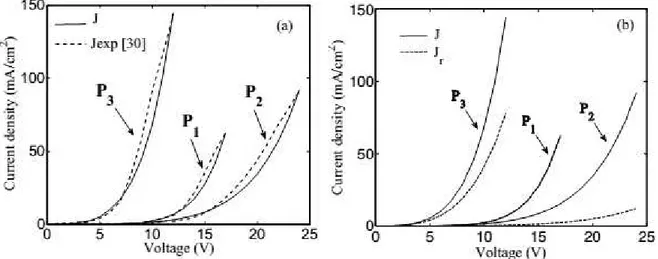
Figure 2 presents the variation of the current density as a function of the applied voltage for P1,
P2 and P3. Fig.2 (a) shows the simulated J-V characteristics, and we see that the simulated results are in good agreement with experimental data from [30]. Fig.2 (b) shows current density J (lines) and
recombination current density Jr (dash) versus applied voltage, the curves of Jr and J fall nearly on top
of one another for P1, P2 and P3, the recombination current density is lower especially for P2. The carriers mobility for the three devices are shown in Fig. 3.
Fig.2 (a) Calculated device current density J (solid) and experimental current density Jexp from Ref. [30] (dash) vs. applied voltage. And Fig.2.(b) Device (solid) and recombination current densities Jr (dash) vs. applied voltage are shown for P1, P2
and P3.
Fig.3 Calculated distributions of mobilities for the three devices: P1 (solid), P2 (dash) and P3 (dots).
We consider these structures “electron only” devices as they have electrons injected from an
and electrons barriers smaller compared to the other two devices. The mobility at the interface
cathode/polymer (x=L), where electrons are injected, is lower by 3 orders of magnitude compared to
the mobility at the interface anode/polymer (x=0), where holes are injected, as seen from Fig.3. This
device has an easy injection of the less mobile electrons and a more or less difficult injection of the
more mobile holes, this leads to a more balanced combination of injection and transport carriers
compared to the other two devices, and as a result, the recombination current density is equal to the
device current density. P2 has higher electrons and holes barriers, and equal mobilities (Fig 3), so it
requires a higher applied voltage. This leads to an unbalanced combination of injection and transport
mechanisms and that is why the recombination current density is too low. The third device P3 has an
electron barrier between the two, a hole barrier close to that of P2, and a higher mobility which ensures a better transport mechanism leading to a lower applied voltage. In this case, the injection and
the transport of carriers are more balanced reducing the shift between J and Jr.
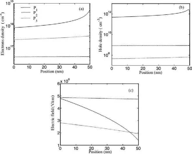
Figure 4 presents carriers (electrons and holes) densities and electric field distributions for P1
(solid), P2 (dash) and P3 (dot). Electrons and holes densities distributions are shown in Fig.4 (a) and
(b) respectively and the electric field distributions in fig.4(c).
From Fig.4 (a) and (b), the electrons density of the three devices is much higher than that of holes
because of the electrons barriers that are too low compared with holes barriers.
In P1, because of the electrons barrier being too low compared with holes one, the carriers densities are accumulated at cathode/ organic layer interface, leading to a variable and higher electric field
(Fig.4(c)) and carriers distributions. In the case of P2 and P3, The electrons and holes barriers are
higher compared with P1; hence the carriers densities are not only decreased but also more uniform.
From Fig.4 (c), the electric field is less variable for P3 as there is an accumulation at the cathode/electrode interface (Fig 4(a)). As for P2, the electric field is higher because of the applied voltage and more uniform as there is no accumulation of the carriers densities.
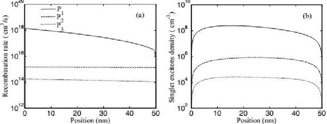
Figure 5 shows the Langevin recombination rates (a) and singlet exciton density profiles (b) for
P1 (solid), P2 (dash) and P3 (dot).
Fig.5. Langevin recombination rate (a) and Singlet exciton density profiles (b). Lines are for P1 (solid), P2 (dash) and P3
(dot).
From Fig.5 (a), the recombination rates are uniform across the device except for P1, but lower by 6, 9
and 10 orders of magnitude for P1, P2 and P3 respectively compared to other PPV derivatives
materials [12], [38].
Similar results were obtained for a hole only device [12] (single carrier device) and because of the
electron barriers lower than the hole ones, our devices are essentially electron only devices. The
non-uniformity of P1 is due to the non-uniformity of the electric field which affects the mobility as seen in
Fig 3. P2 and P3 have higher electron mobility with a harder injection of holes, unbalancing the combination of injection and transport mechanisms, lowering the recombination rate for these devices.
When electrons and holes meet, they form singlet and triplet excitons, 25% of which recombine
radiatively and 75% non-radiatively respectively, as a result, a very low singlet excitons density
(Fig.5(b)).
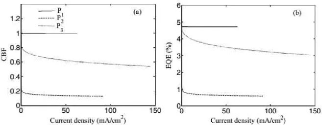
B. Device efficiency
Fig.6. Calculated recombination efficiency (a) and external quantum efficiency (b) vs. device current density. Lines are for P1 (solid), P2 (dash) and P3 (dot).
Fig.6 (a) and (b) show that the CBF and the EQE are the highest for the first device P1 and the lowest
for P2. These devices present a difficult injection of the more mobile holes and easy injection of the less mobile electrons, somewhat balancing the injection and transport mechanisms. The injected
carriers accumulate in the vicinity of the cathode/ organic layer interface because of the low mobility,
whereas, because of the higher barrier, the holes accumulate at the vicinity of the anode/ organic layer
interface. The low electrons barrier and the high holes mobility, reduces the accumulation of both
carriers near their respective interfaces, hence improving the CBF and EQE (even if the EQE increase
is less than 5 % which is the case for all PPV's based materials [39] – [41]). P2 has electrons and holes
injected from an ohmic contact and contact limited contact respectively with equal mobilities (Fig.3),
leading to the accumulation of holes near its interface. The combination of injection/ transport
mechanism is deeply imbalanced lowering the CBF and consequently the EQE.
Figure 7 shows the recombination power efficiency CBFp (a) and the external quantum power
efficiency EQEp (b) versus device current density for P1 (solid), P2 (dash) and P3 (dot).
Fig.7 Recombination power efficiency (a) and external power efficiency (b) vs. device current density. Lines are for P1
The recombination power efficiency (ratio of output to input power) is lower for the second device
P2 because a high voltage is applied. In the case of P3, a low voltage is applied, as a result, the CBFp value is higher, while for P1, an intermediate applied voltage yields to a CBFp value between the two.
As a result, the EQEp which depends on the CBFp has similar trend even if its largest value is 5%.
In spite of these results, it is noticed that this model presents some limitations since it is derived
from inorganic semiconductors physics and as the organic semiconductors have disordered molecular
structures or even amorphous unlike the inorganic ones which have a crystalline structure.
From this physical modeling, we know now that balancing injection and transport mechanisms
ensures a better PLEDs efficiency; however, that is not always possible. The injection mechanism
would be more efficient by reducing the height barriers at both interfaces as much as possible; the
main idea is to match the electrode material with the electronic structure of the electroluminescent
polymer. Nevertheless, when the barrier height is too small, less than a tenth of electron volts, the
barrier will not have a triangular form as the model assumes, so the electron will not tunnel, and the
thermionic emission phenomena becomes too important. In addition, the evaporated electrodes will
not have the outlined work-function values listed from literature, as they are full of defects. The
transport mechanism which is ensured mainly by carriers mobility and the space charge limited effects
would also be influenced as the barriers are too small [42]. Another problem with modeling is that the
experimental data does not always fit with the physical model described above, in some cases, the
match is only for a small region and the model here would be considered inapplicable, and in some
other cases, the fit is for a large region [43], and here, the model can be considered unfailing.
Another drawback, is that sometimes, organic semiconductors electronic structures can’t be well
matched with electrodes material since the barriers are too high, and in this case, an efficient injection
via Fowler Nordheim tunneling will not be possible anymore, so in order to overcome this, hole
or/and electrons blocking layer is added between electrode(s) and the emitting polymer [42]. This
layer, blocks the majority carriers (electrons or/ and holes), where they are increased at the interface of
the blocking layer and a strong internal electric field is created by the minority carriers side, which
balance electrons and holes current densities.
To ameliorate injection efficiency, impurities or defects are added, electrons or holes acceptor
groups are end-capped which allow electron tunneling or these groups are incorporated into the
polymeric chain thus copolymers are created.
In general, one should be aware that up until now, no perfect model exists to describe the electrical
and optical characteristics for theses kind of devices [43]. As a matter of fact, we just have to choose
V. CONCLUSIONS
This paper has clearly presented an in depth understanding of DP-PPV's based devices by studying
the injection, transport and recombination mechanisms.
From the research that has been carried out, it is possible to conclude that P1 has the best performance among these devices, as it has the best injection barriers, which affects greatly the
recombination current density; if the barriers are too high, the recombination current density drops
excessively. We have seen also that the best device performance is insured by the balance between the
injection and transport mechanisms: either contacts and high mobilities or ohmic contacts with low
mobility and contact limited contact with high mobility. As a matter of fact, this balance affects the
recombination efficiency resulting in a best CBF and external quantum efficiency EQE values for P1
device. These two parameters drop as the combination injection/ transport is imbalanced.
The obtained values of the recombination power efficiency are inversely proportional to the
applied voltage as expected, the best CBFp value was for device P3, since it has the lowest applied
voltage. This low voltage requirement depends on height barriers, carrier’s mobility and polymer layer
thickness: if the combination injection/ transport is well balanced, the required applied voltage will be
lower and vice versa.
ACKNOWLEDGEMENTS
The authors would like to thank the precious and fundamental help of Dr. S.Labiod and Mr.
A.Meziani for the guidance, correction and proofreading this paper. This work has been funded by the
Algerian ministry of higher education and scientific research.
REFERENCES
[1] C. Zhang, P. Chen and W. Hu, “ Organic field-effect transistor-based gas sensors “, Chem. Soc.
Rev., 44, pp. 2087-2107, 2015.
[2] Junmo Kang, Deep Jariwala, Christopher R Ryder, Spencer A Wells, Yongsuk Choi, Euyheon
Hwang, Jeong Ho Cho, Tobin J. Marks, and Mark C Hersam, “Probing out-of-plane charge
transport in black phosphorus with graphene-contacted vertical field-effect transistors”, ACS
Nano, 16 (4), pp 2580–2585, 2016.
[3] Xiu-Li Yang , Xiahui Chen , Gui-Hua Hou , Rong-Feng Guan , Rong Shao , and Ming-Hua
Xie, “A multiresponsive metal–organic framework: direct chemiluminescence,
photoluminescence, and dual tunable sensing applications”, Adv. Funct. Mater. 26, pp. 393–398, 2016.
[4] Dian Zhao, Yuanjing Cui, Yu Yang and Guodong Qian, “Sensing‐functional luminescent metal‐
organic frameworks”, CrystEngComm, ,18, pp. 3746-3759, 2016.
[5] Timothy F. O’Connor, Aliaksandr V. Zaretski, Suchol Savagatrup, Adam D. Printz, Cameron D.
high cyclic bending stability: Materials selection criteria”, Solar Energy Materials & Solar Cells,
144, pp. 438–444, 2016.
[6] Maxime Guérette , Ahmed Najari , Julie Maltais , Jean-Rémi Pouliot , Stéphane Dufresne ,
Martin Simoneau , Simon Besner , Patrick Charest , and Mario Leclerc, “New processable
phenanthridinone-based polymers for organic solar cell applications”, Adv. Energy Mater., 6,
pp.1-6 (1502094). 2016
[7] Ideki Shirakawa, Edwin J. Louis, Alan G. Macdiarmid, Chwan K. Chiang, and Alan J. Heeger,
“Synthesis of electrically conducting organic polymers : halogen derivatives of polyacetylene, (CH)x”, J.Chem. Soc., Chem. Commun., pp. 578-580, 1977.
[8] C. W. Tang and S. A. VanSlyke, “Organic electroluminescent diodes”, Appl. Phys. Lett. vol.51,
no. 12, pp. 913-915, 21 September 1987.
[9] I.D. Parker, “Carrier tunneling and device characteristics in polymer light-emitting diodes”, J.
Appl. Phys. Vol.75, no. 3, pp. 1656-1666, 1 February 1994.
[10] P. S. Davids, Sh. M. Kogan, I. D. Parker, and D. L. Smith, “Charge injection in organic light
-emitting diodes: Tunneling into low mobility materials”, Appl. Phys. Lett., vol. 69, no. 15, pp.
2270-2272, 7 October 1996.
[11] P. S. Davids, I. H. Campbell, and D. L. Smith, “Device model for single carrier organic diodes”
J. Appl. Phys., vol.82, no. 12, pp. 6319-6325, 15 December 1997.
[12] B. K. Crone, P. S. Davids, I. H. Campbell, and D. L. Smith, “Device model investigation of
single layer organic light emitting diodes” , J. Appl. Phys., vol.84, no. 2, pp. 833-82, 15 July 1998.
[13] B. K. Crone, I. H. Campbell, P. S. Davids, and D. L. Smith, “Charge injection and transport in
single-layer organic light-emitting diodes” , Appl. Phys. Lett., vol. 73, no. 21, pp. 3162-3164,
23 November 1998.
[14] B. K. Crone, I. H. Campbell, P. S. Davids, D. L. Smith, C. J. Neef et al., “Device physics of
single layer organic light-emitting diodes”, J. Appl. Phys. vol. 86, no. 10, pp. 5767- 5774, 15
November 1999.
[15] B. K. Crone, P. S. Davids, I. H. Campbell, and D. L. Smith, “Device model investigation of
bilayer organic light emitting diodes”, J. Appl. Phys. vol. 87, no. 4, pp. 1974-1982, 15 February 2000.
[16] Aline P. Roque, Luiza A. Mercante, Vanessa P. Scagion, Juliano E. Oliveira,Luiz H. C.
Mattoso, Leonardo De Boni, Cleber R. Mendonca, Daniel S. Correa, “Fluorescent
PMMA/MEH-PPV electrospun nanofibers: investigation of morphology, solvent, and surfactant
effect”, JOURNAL OF POLYMER SCIENCE, PART B: POLYMER PHYSICS, vol. 50, pp.
1388–1394, 2014.
[17] Jie Li , Tetsuya Nakagawa , Qisheng Zhang , Hiroko Nomura , Hiroshi Miyazaki , and
activated delayed fluorescence channel in a heptazine derivative”, Adv. Mater., Vol.25, Issue
24, pp. 3319–3323, 2013.
[18] Ning Li, Satoshi Oida, George S. Tulevski, Shu-Jen Han, James B. Hannon, Devendra K.
Sadana, Tze-Chiang Chen, “Efficient and bright organic light-emitting diodes on single-layer
graphene electrodes”, Nature Communications 4, 2294, pp. 1-7, 2013.
[19] Xiao Huang, Zhiyuan Zeng, Zhanxi Fan, Juqing Liu, and Hua Zhang, “Graphene-based
electrodes”, Adv. Mater., vol. 24, Issue 45, pp. 5979–6004, 2012.
[20] Jeonghun Kwak, Wan Ki Bae, Donggu Lee, Insun Park, Jaehoon Lim, Myeongjin Park,
Hyunduck Cho,Heeje Woo, Do Y. Yoon, Kookheon Char,Seonghoon Lee, and Changhee Lee,
“Bright and efficient full-color colloidal quantum dot light-emitting diodes using an inverted
device structure”, Nano Lett., vol. 12, pp. 2362−2366, 2012.
[21] Jing Gao, Xue Mu, Xiao-Yun Li, Wen-Yi Wang, Yan Meng, Xiao-Bing Xu, Ting Chen,
Li-Jun Cui, Xiaoming Wu, and Hong-Zhang Geng, “Modification of carbon nanotube transparent
conducting films for electrodes in organic light-emitting diodes”, Nanotechnology, vol.24,
43520, pp. 1-8, 2013.
[22] Lu Lian, Dan Dong, Shuai Yang, Bingwu Wei, and Gufeng He, “highly conductive and uniform
alginate/silver nanowire composite transparent electrode by room temperature solution
processing for organic light emitting diode”, ACS Applied Materials & Interfaces, vol. 9, no.13,
pp 11811–11818, 2017.
[23] Hung-Chi Chen, Jiun-Haw Lee,Member, IEEE, Chia-Chiang Shiau, Chih-Chung Yang,Senior
Member, IEEE, and Yean-Woei Kiang,Member, IEEE, “Electromagnetic modeling of organic
light-emitting devices”, journal of lightwave technology, vol. 24, no. 6, pp. 2450-2457, 2006.
[24] C. K. F. Weilerand S. Körkel, “Optimum experimental design for extended Gaussian disorder
modeled organic semiconductor devices”, J. Appl. Phys. vol. 113, 094903, pp. 1-6, 2013. [25] U. Wolf, V. I. Arkhipov, and H. Bassler, “Current injection from a metal to a disordered
hopping system. I. Monte Carlo simulation”, PHYSICAL REVIEW B, vol. 59, no. 11, pp.
7505-7513, 15 March 1999.
[26] H. Razafitrimo a, Y. Gao a, W.A. Feld b, B.R. Hsieh, “A layer-wise topographic study of
a polymeric light-emitting diode: indium-tin oxide / poly ( 2,3-diphenyl-p-phenylene
vinylene) / Ag”, Synthetic Metals, vol. 79, pp. 103-106, 1996.
[27] Wen-Liang Yeh, Hsin-Lung Chen, Show-An Chen, “Synthesis and spectral characterizations of
electroluminescent poly(2,3-di-[p-(2-ethylhexoxy)phenyl]-1,4-phenylenevinylene)”, Synthetic
Metals, vol. 157, pp. 407–413, 2007.
[28] Yu-Chun Wu, Xiang-Kui Ren, Er-Qiang Chen, Hsun-Mei Lee, Jean-Luc Duvail, Chien-Lung
Wang, and Chain-Shu Hsu, “Preservation of Photoluminescence Efficiency in the Ordered
π−πInteractions with Dendritic Aliphatic Side Chains”, Macromolecules, vol. 45, pp. 4540−4549, 2012.
[29] Yung-Ming Liao, Hung-Min Shih, Kuang-Hui Hsu, Chain-Shu Hsu, Yu-Chiang Chao,
Sheng-Chia Lin, Chun-Yao Chen, Hsin-Fei Meng, “High-performance
poly(2,3-diphenyl-1,4-phenylene vinylene)-based polymer light-emitting diodes by blade coating method”, Polymer,
vol. 52, pp. 3717-3724, 2011.
[30] Sheng-Hsiung Yang, Jiun-Tai Chen, An-Kuo Li, Chun-Hao Huang, Kuei-Bai Chen, Bing-R.
Hsieh, Chain-Shu Hsu,” New soluble poly(2,3-diphenylphenylene vinylene) derivatives for
light-emitting diodes”, Thin Solid Films, vol. 477, pp. 73 – 80., 2005.
[31] Yung-Ming Liao, Hung-Min Shih, Kuang-Hui Hsu, Chain-Shu Hsu, Yu-Chiang Chao,
Sheng-Chia Lin, Chun-Yao Chen, Hsin-Fei Meng,” High-performance
poly(2,3-diphenyl-1,4-phenylene vinylene)-based polymer light-emitting diodes by blade coating method”, Polymer,
vol. 52, pp. 3717-3724, 2011.
[32] Jiun-Tai Chen, Chain-Shu Hsu,”Poly(2,3-diphenyl-1,4-phenylenevinylene) (DP-PPV)
derivatives: Synthesis, properties, and their applications in polymer light-emitting diodes”,
Polymer, vol. 54, pp. 4045-4058, 2013.
[33] Chang S. M.; Su P. K.; Lin G. J. and Wang T. J., “Bluish-green to orange-red flexible
light-emitting devices using copolymers of DP6-PPV and MEH-PPV”, Synthetic Metals, vol. 137,
pp. 1025–1026, 2003.
[34] E. Ettedgui, H. Razafitrimo, and Y. Gao, “Evidence for the Formation of Unoccupied States in
Poly(2,3-Diphenylphenylene Vinylene) Following the Deposition of Metal”, Physical Review
Letters, vol.76, no.2, pp. 299-302, 1996.
[35] J. Hromcova, D. Donoval, And J. Rack, “Numerical Simulation of a Metal
-Semiconductor-Metal Structure with Schottky Contacts at Both Ends”, phys. stat. sol. (a), vol. 142, pp. 167 -175, 1994.
[36] Fei-ping Lu, Xiao-bin Liu, and Yong-zhong Xing, “Numerical study of the influence of applied
voltage on the current balance factor of single layer organic light-emitting diodes”, Journal of
Applied Physics, vol. 115, pp. 164508 (1-6), 2014.
[37] Wolfgang Brutting, Jorg Frischeisen, Tobias D. Schmidt, Bert J. Scholz, and Christian Mayr,
“Device efficiency of organic light-emitting diodes: Progress by improved light out coupling”,
Phys. Status Solidi A, pp. 1–22, 2012.
[38] H. Siemund, F. Bröcker, and H. Göbel, “Enhancing the electron injection in polymer
light-emitting diodes using a sodium stearate/aluminum bilayer cathode”, Organic Electronics, vol.
14, pp. 335–343, 2013.
[39] G. G. Malliaras and J. C. Scott, “Numerical simulations of the electrical characteristics and the
efficiencies of single-layer organic light emitting diodes”, J. Appl. Phys. vol.85, no.10, pp.
[40] Y. Kawabe, M. M. Morrell, G. E. Jabbour, S. E. Shaheen, B. Kippelen et al, “A numerical study
of operational characteristics of organic light-emitting diodes”, Journal Of Applied Physics, vol.
84, no. 9, pp. 5306-5314, 1998.
[41] Y.D. Jin, J.P. Yang, P.L. Heremans, M. Van der Auweraer, E. Rousseau, H.J. Geise, G. Borghs,
“Single-layer organic light-emitting diode with 2.0% external quantum efficiency prepared by
spin-coating”, Chemical Physics Letters, vol. 320, pp.387–392, 2000.
[42] Prof. Wenping Hu, Organic Electronics, Germany, Wiley-VCH Verlag GmbH & Co. KGaA,
Boschstr, 2013, p. 294-296.
[43] L. Pareira, Organic light emitting diode: The use of rare-earth and transition metals. New