Volume 2013, Article ID 160464,5pages http://dx.doi.org/10.1155/2013/160464
Research Article
Effect of a Polymeric Protective Coating on Optical and
Electrical Properties of Poly(
p
-phenylene vinylene) Derivatives
V. C. Gonçalves,
1C. A. Olivati,
2A. J. F. Carvalho,
3and D. T. Balogh
11Instituto de F´ısica de S˜ao Carlos (IFSC), USP, CP 369, CEP 13566-590 S˜ao Carlos, SP, Brazil
2Faculdade de Ciˆencia e Tecnologia (FCT), Unesp Presidente Prudente, CP 467, CEP 19060-900 Presidente Prudente, SP, Brazil
3Departamento de Engenharia de Materiais, Escola de Engenharia de S˜ao Carlos (EESC), USP, CP 359,
CEP 13566-590 S˜ao Carlos, SP, Brazil
Correspondence should be addressed to C. A. Olivati; [email protected] Received 14 August 2013; Revised 26 September 2013; Accepted 29 September 2013 Academic Editor: Jiamin Wu
Copyright © 2013 V. C. Gonc¸alves et al. his is an open access article distributed under the Creative Commons Attribution License, which permits unrestricted use, distribution, and reproduction in any medium, provided the original work is properly cited. he resistance to photodegradation of poly[(2-methoxy-5-n-hexyloxy)-p-phenylene vinylene] (OC1OC6-PPV) ilms was signii-cantly enhanced by the use of poly(vinyl alcohol) 99% hydrolyzed as protective coating. he deposition of poly(vinyl alcohol) onto OC1OC6-PPV ilms did not afect the absorption and the emission spectra of the luminescent polymer. he protected ilm showed 5% drop on the absorbance at 500 nm ater 270 hours of light exposure while the unprotected ilm completely degraded in the same conditions. he conductivity of the protected ilm remained stable (around7 × 10−10S/m) while the value for the unprotected one dropped around two orders of magnitude ater 100 hours of light exposure.
1. Introduction
Poly(p-phenylene vinylene), PPV, derivatives have been widely explored for applications in optoelectronics such as photoluminescent devices, light-emitting diodes, and sensors [1–3]. Despite their wide range of possible applications, the PPV derivatives are highly susceptible to photodegra-dation, by the combined action of light and oxygen. he photodegradation reaction involves mainly the vinyl group, leading to the formation of carbonyl groups, reducing the conjugation length and, in further stages, leading to chain scission [4–14]. he photodegradation occurs in solution or in the solid state, causing a decay in the absorbance intensity and a blue shit in the absorbance and, consequently, in the emission spectrum of the polymer. In solid state, the photodegradation is thickness dependent due to mainly two factors. he irst factor is the diference in the light intensity through the thickness of the material due to the light absorption. he light intensity should be maximum at the surface and decrease exponentially with the increase in thickness (Lambert’s law) [15]. he second factor is
the oxygen concentration throughout the material, which depends on the oxygen difusion through the ilm [11]. Some approaches have been used in order to prevent or at least try to minimize the photodegradation in the PPV derivatives. An alternative is the use of diferent encapsulations [16–
2. Experimental
Cast ilms of OC1OC6-PPV (ca. 300–400 nm thickness) were deposited onto glass substrates, indium tin oxide (ITO) or interdigitated chromium-gold array at room temperature in the dark [22] from chloroform solutions (0.3 mg/mL). he PVA coatings were prepared by dipping the samples into a 2 wt% solution of PVA 99% hydrolyzed in ethanol-water mixture and drying them under reduced pressure at 40∘C, yielding � ≈ 1 �m layer. he gold array was prepared by lit-of lithography with 100 lines of 5 mm length electrodes with 100 nm of thickness, separated by 10�m of distance. Photodegradation experiments were performed with a white light from a halogen lamp (50 W, 12 V-Osram) placed at a ixed distance from the samples, yielding 17 mW/cm2 of power at the sample surface. hese irradiations were per-formed at room atmosphere at 25∘C. UV-Vis absorption measurements were carried out in a HITACHI U-2001 spec-trophotometer in the range between 400 and 650 nm. he emission spectra of the ilm (�exc = 490 nm) and the emis-sion spectra of the device (current applied = 6 mA) were recorded in a Shimadzu 5301 PC spectroluorimeter. All ilms used in the photodegradation measurements presented the same optical density in order to avoid the efect of ilm thicknesses on photodegradation. he device used to record the electroluminescence spectra was ITO/OC1OC6-PPV/Al; the OC1OC6-PPV active layer was made of cast ilm from 0.25 mg/mL chloroform solution (ca. 300 nm). In this case, the PVA layer was applied over the aluminum layer. A 90 nm thick Al cathode was vacuum evaporated (10−6Torr) and with an active area for the devices of 0.12 cm2. he electrical behavior was carried out by measuring the current versus voltage at room conditions with a Keithley238 high voltage source-measure unit.
3. Results
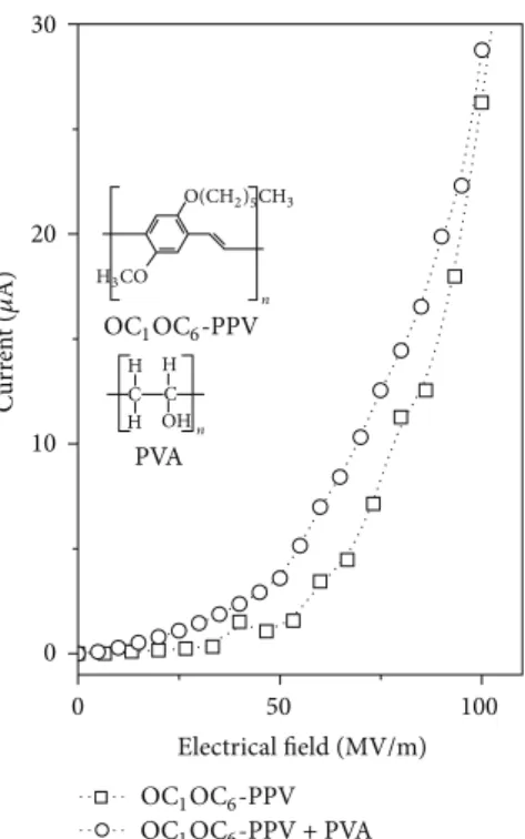
he characteristic current versus electrical ield curves do not show signiicant diferences with the use of PVA as coating, as shown inFigure 1. he onset voltage of the device coated with PVA was around 5 V, which is similar to other devices of OC1OC6-PPV made from cast ilms and the same coniguration [23–25].
he absorption in the visible region of the cast ilms with and without the PVA coating showed no signiicant diferences, and the maximum wavelengths of absorption are at 500 nm (Figure 2). he same result was obtained for the photoluminescence (PL) and electroluminescence (EL) spectra of these ilms, as also shown inFigure 2and its inset. he emission wavelength of the zero-phonon transition was about 590 nm for all samples. It is worth to note that the values of absorbance, PL and EL, of protected ilm are nearly the same of the neat ilm since the protective coating is completely transparent and does not absorb or have emission on the visible range and all the ilm production and the coating processes are performed in dark. Extreme care should be taken to reproduce intensity values of the photo- and electroluminescence spectra of OC1OC6-PPV because even
0 50 100
0 10 20 30
Electrical ield (MV/m)
OC1OC6-PPV
OC1OC6-PPV
OC1OC6-PPV + PVA
O(CH2)5CH3
H3CO
n n H H H C C OH PVA C ur ren t ( � A)
Figure 1: Current versus electrical ield of ITO/OC1OC6-PPV/Al, neat and coated with PVA.
0.0 0.2 0.4 0.6 0.8 1.0
400 500 600 700 800 900
0.0 0.2 0.4 0.6 0.8 1.0
500 600 700 800 900 0.0 0.2 0.4 0.6 0.8 1.0 PL in te n si ty (a.u .) ABS (a.u .) EL in ten si ty (a.u .) �(nm) �(nm) OC1OC6-PPV
OC1OC6-PPV + PVA
Figure 2: Visible, photoluminescence, and electroluminescence spectra of OC1OC6-PPV ilms with and without a PVA coating. he electroluminescence spectra were carried out onto ITO/OC1OC6 -PPV/Al (neat and coated with PVA).
the ambient light degrades the neat ilm. Also, very short exposures to the excitation light have to be used to record the photoluminescence spectra of these ilms in ambient conditions.
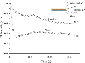
he electroluminescence of two single layer devices of OC1OC6-PPV (ITO/OC1OC6-PPV/Al), neat and coated with poly(vinyl alcohol) over the aluminum layer (as in inset
ofFigure 3), was recorded continuously for 300 seconds at
1.0 0.8 0.6 0.4 0.2 0.0
0 100 200 300
Time (s) Coated Neat 60% 40% Poly(vinyl alcohol) Al ITO Glass
OC1OC6-PPV
EL in te n si ty (a.u .)
Figure 3: Normalized electroluminescence decay for the ITO/OC1OC6-PPV/Al cast ilm and ITO/OC1OC6-PPV/Al cast ilm coated with PVA. he lines are only to guide the eyes.
contacts. Ater 150 seconds of stabilization, the coated device presented 60% of the initial emission intensity while the neat one presented just 40%. Studies on the efects of the luminance and lifetime of the devices are subject of future works. For single layer devices, interface and Joule efects are more pronounced in long-term experiments which is required for lifetime studies, turning the results more compli-cated to analyze properly. Build-up of multilayer devices can introduce more variables in the analysis turning the system even more complicated to reach a clear conclusion. herefore, long-term experiments of light exposure were performed only with optical and conductivity measurements and not with the devices.
he absorption spectra of OC1OC6-PPV cast ilm with-out the poly(vinyl alcohol) coating, taken ater several peri-ods of exposure to the white light, showed a behavior similar to the one observed in earlier reports [13,14]. he absorbance initially decreases without changing the line shape of the spectra or the wavelength of maximum absorbance and, in a further step of the degradation, the spectra are blue shited while continuously decreasing the maximum absorbance values [14]. However, when the cast ilm is coated with poly(vinyl alcohol), the changes in the spectra are drasti-cally reduced, and, in the same period of irradiation, the decrease in the absorbance values was about 5%, while in the same period the nonprotected OC1OC6-PPV ilm was completely degraded. his efect is clearly seen by plotting the normalized absorbance values at 500 nm (wavelength of maximum absorption of the nondegraded OC1OC6-PPV) in function of the irradiation time as shown inFigure 4. his igure shows the results of the ilm coated with poly(vinyl alcohol) in function of the continuous exposure of the ilm to the white light till 620 hours, showing a total decrease of ca. 12% of the absorbance values. he inset ofFigure 4shows the kinetic plot from which the photodegradation rates could be estimated, being two orders of magnitude lower for the coated ilm: ca.4 × 10−2h−1 and2 × 10−4h−1, respectively, for the neat ilm and the ilm coated with PVA. It is very important
0 100 200 300 400 500 600 700
0.00 0.20 0.40 0.60 0.80 1.00
0 100 200 300 400 500 600 0.000 0.001 0.002 0.007 0.018 0.050 0.135 0.368 1.000
Exposure time (h)
Exposure time (h)
OC1OC6-PPV
OC1OC6-PPV + PVA
ABS/ABS 0 A− A00 /A 0 −A 00
Figure 4: Normalized absorbance decay for the OC1OC6-PPV cast ilm and OC1OC6-PPV cast ilm coated with PVA, irradiated with white light. he inset shows the kinetic plot (�-axis in log scale) for the same samples. he lines are only to guide the eyes.
to emphasize that these estimated values are only valid for samples with thicknesses of ca. 300–400 nm since there is a strong dependence between the absorbance decay rates and the ilm thickness.
Similar protecting efect of the PVA coating against OC1OC6-PPV photodegradation can also be seen in the photoluminescence characterization. he PL intensity of the pure ilm drops 50% in the irst 40 minutes of exposure, while the intensity for the coated one remains the same.
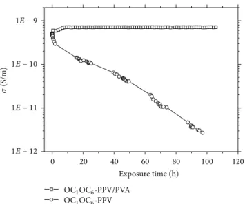
For the conductivity measurements, a constant voltage of 6 V was applied for several hours at room conditions while exposing the ilms under the electrodes to the white light and measuring the current at diferent time intervals. he conduc-tivity measurements showed that the cast ilms coated with PVA presented a more stable conductivity than that observed for neat OC1OC6-PPV ilms (Figure 5). he conductivity values obtained for the PVA-protected OC1OC6-PPV ilm deposited onto an interdigitated chromium-gold array under the illumination remain constant (around 7 × 10⁻¹⁰S/m) for at least 100 hours of continuous light exposure. For the unprotected OC1OC6-PPV, the conductivity decreased two orders of magnitude in the same exposure period (from4.5 ×
10−10S/m to2.5 × 10−12S/m).
4. Conclusions
0 20 40 60 80 100 120 Exposure time (h)
OC1OC6-PPV/PVA
OC1OC6-PPV
1E − 9
1E − 10
1E − 11
1E − 12
𝜎
(S/m)
Figure 5: Conductivity values of the OC1OC6-PPV cast ilm and OC1OC6-PPV cast ilm coated with PVA, measured in an interdigitated electrode and irradiated with white light. he lines are only to guide the eyes.
optimization of fabrication, can be used in applications such as sensors and FETs, among others.
Acknowledgments
he inancial support of Conselho Nacional de Desen-volvimento Cient´ıico e Tecnol´ogico (CNPq), Fundac¸˜ao de Amparo `a Pesquisa do Estado de S˜ao Paulo (FAPESP), Coordenac¸˜ao de Aperfeic¸oamento de Pessoal de N´ıvel Supe-rior (CAPES), and Instituto Nacional de Eletrˆonica Orgˆanica, Brazil is acknowledged.
References
[1] J. H. Burroughes, D. D. C. Bradley, A. R. Brown et al., “Light-emitting diodes based on conjugated polymers,”Nature, vol. 347, pp. 539–541, 1990.
[2] N. C. Greenham, S. C. Moratti, D. D. C. Bradley, R. H. Friend, and A. B. Holmes, “Eicient light-emitting diodes based on polymers with high electron ainities,”Nature, vol. 365, no. 6447, pp. 628–630, 1993.
[3] F. Hide, M. A. D´ıaz-Garc´ıa, B. J. Schwartz, M. R. Andersson, Q. Pei, and A. J. Heeger, “Semiconducting polymers: a new class of solid-state laser materials,”Science, vol. 273, no. 5283, pp. 1833– 1836, 1996.
[4] B. H. Cumpston and K. F. Jensen, “Photo-oxidation of electro-luminescent polymers,”Trends in Polymer Science, vol. 4, no. 5, pp. 151–157, 1996.
[5] G. H. Gelinck and J. M. Warman, “he efect of photo-oxidation on the photo-conductivity of isolated polyphenylenevinylene chains,”Chemical Physics Letters, vol. 277, no. 4, pp. 361–366, 1997.
[6] F. J. J. Janssen, L. J. Van IJzendoorn, H. F. M. Schoo et al., “Degra-dation efects in poly para-phenylene vinylene derivatives due to controlled oxygen exposure,”Synthetic Metals, vol. 131, no. 1– 3, pp. 167–174, 2002.
[7] W. Holzer, A. Penzkofer, M. Pichlmaier, D. D. C. Bradley, and W. J. Blau, “Photodegradation of some luminescent polymers,”
Chemical Physics, vol. 248, no. 2-3, pp. 273–284, 1999.
[8] H. Y. Low, “Photo and photo-oxidative degradations of poly(phenylene vinylene) derivatives,”hin Solid Films, vol. 413, no. 1-2, pp. 160–166, 2002.
[9] B. H. Cumpston and K. F. Jensen, “Photo-oxidation of polymers used in electroluminescent devices,”Synthetic Metals, vol. 73, no. 3, pp. 195–199, 1995.
[10] G. D. Hale, S. J. Oldenburg, and N. J. Halas, “Efects of photo-oxidation on conjugated polymer ilms,”Applied Physics Letters, vol. 71, no. 11, pp. 1483–1485, 1997.
[11] A. Alba Garc´ıa, H. Schut, L. D. A. Siebbeles, and A. Van Veen, “Depth proiling of the degradation of OC1OC10-PPV monitored by positron beam analysis,”Synthetic Metals, vol. 138, no. 1-2, pp. 43–47, 2003.
[12] R. F. Bianchi, D. T. Balogh, M. Tinani, R. M. Faria, and E. A. Irene, “Ellipsometry study of the photo-oxidation of Poly[(2-methoxy-5-hexyloxy)-p-phenylenevinylene],”Journal of Poly-mer Science, Part B, vol. 42, no. 6, pp. 1033–1041, 2004. [13] F. M. Marconi, R. F. Bianchi, R. M. Faria, and D. T. Balogh,
“Solvent efects on the photodegration of a PPV derivative,”
Molecular Crystals and Liquid Crystals Science and Technology Section A, vol. 374, pp. 475–480, 2002.
[14] C. A. Olivati, M. Ferreira, R. F. Bianchi, R. M. Faria, O. N. Oliveira Jr., and D. T. Balogh, “he inluence of preparation method of OC1OC6-PPV ilms on the photo-oxidation pro-cess,”Polymer Degradation and Stability, vol. 91, no. 10, pp. 2342–2346, 2006.
[15] F. H. Lohman, “he mathematical combination of Lambert’s law and Beer’s law,”Journal of Chemical Education, vol. 32, no. 3, p. 155, 1955.
[16] V. C. Gonc¸alves, A. J. F. Carvalho, and D. T. Balogh, “Polymeric coatings for photostability enhancement of poly(p-phenylene vinylene). derivative ilms,”Polymer International, vol. 59, no. 5, pp. 637–641, 2010.
[17] H.-C. Lee, T.-W. Lee, Y. T. Lim, and O. O. Park, “Improved environmental stability in poly(p-phenylene vinylene)/layered silicate nanocomposite,”Applied Clay Science, vol. 21, no. 5-6, pp. 287–293, 2002.
[18] B. H. Cumpston and K. F. Jensen, “Photooxidative sta-bility of substituted poly(phenylene vinylene) (PPV) and poly(phenylene acetylene) (PPA),”Journal of Applied Polymer Science, vol. 69, no. 12, pp. 2451–2458, 1998.
[19] P. Le Rendu, T. P. Nguyen, and L. Carrois, “Cellulose acetate and PVDC used as protective layers for organic diodes,”Synthetic Metals, vol. 138, no. 1-2, pp. 285–288, 2003.
[20] J. S. Lewis and M. S. Weaver, “hin-ilm permeation-barrier technology for lexible organic light-emitting devices,” IEEE
Journal on Selected Topics in Quantum Electronics, vol. 10, no.
1, pp. 45–57, 2004.
[21] G. H. Kim, J. Oh, Y. S. Yang, L.-M. Do, and K. S. Suh, “Encapsulation of organic light-emitting devices by means of photopolymerized polyacrylate ilms,”Polymer, vol. 45, no. 6, pp. 1879–1883, 2004.
[22] C. De Almeida Olivati, R. F. Bianchi, F. M. Marconi, D. T. Balogh, and R. M. Faria, “Photoconduction efect on PPV and MH-PPV structures,”Molecular Crystals and Liquid Crystals
Science and Technology Section A, vol. 374, pp. 451–456, 2002.
performance due to an electron-injecting layer of ionomers,”
Chemical Physics Letters, vol. 408, no. 1–3, pp. 31–36, 2005. [24] C. A. Olivati, A. J. F. Carvalho, D. T. Balogh, and R. M. Faria,
“Electrical properties of polymer/metal interface in polymer light-emitting devices: electron injection barrier suppression,”
Submit your manuscripts at
http://www.hindawi.com
Scientifica
Hindawi Publishing Corporation
http://www.hindawi.com Volume 2014
Hindawi Publishing Corporation
http://www.hindawi.com Volume 2014
Hindawi Publishing Corporation
http://www.hindawi.com Volume 2014
Hindawi Publishing Corporation
http://www.hindawi.com Volume 2014
Ceramics
Journal ofHindawi Publishing Corporation
http://www.hindawi.com Volume 2014
Nanoparticles
Journal of Hindawi Publishing Corporationhttp://www.hindawi.com Volume 2014
Hindawi Publishing Corporation
http://www.hindawi.com Volume 2014 International Journal of
Biomaterials
Hindawi Publishing Corporation
http://www.hindawi.com Volume 2014
Nanoscience
Journal ofTextiles
Hindawi Publishing Corporation
http://www.hindawi.com Volume 2014
Journal of Hindawi Publishing Corporation
http://www.hindawi.com Volume 2014
Crystallography
Journal of Hindawi Publishing Corporationhttp://www.hindawi.com Volume 2014
The Scientiic
World Journal
Hindawi Publishing Corporationhttp://www.hindawi.com Volume 2014
Hindawi Publishing Corporation
http://www.hindawi.com Volume 2014
Coatings
Journal ofAdvances in
Materials Science and Engineering
Hindawi Publishing Corporation
http://www.hindawi.com Volume 2014
Hindawi Publishing Corporation
http://www.hindawi.com Volume 2014
Hindawi Publishing Corporation
http://www.hindawi.com Volume 2014
Metallurgy
Journal ofHindawi Publishing Corporation
http://www.hindawi.com Volume 2014
BioMed
Research International
Materials
Journal of Hindawi Publishing Corporationhttp://www.hindawi.com Volume 2014
N
a
no
ma
te
ria
ls
Hindawi Publishing Corporation
http://www.hindawi.com Volume 2014
Journal of