Autor Responsable: Carlos Javier Pereyra Fecha de envío: 17/12/2014 Fecha de aprobación: 05/05/2015 10.1590/S1517-707620150003.0079
Optical absorption enhancement in
sensitized ZnO nanorods
for solar cells
Aumento de la Absorción Óptica en
Nanovarillas de ZnO Sensibilizadas
para Celdas Solares
Carlos Javier Pereyra1, Florencia Ferrer1, Carmela Gómez1,
Lucía Campo1, Ricardo Enrique Marotti1, Francisco Martin2,
Dietmar Leinen2, José Ramos-Barrado2,
Enrique Ariel Dalchiele1
1 Instituto de Física & CINQUIFIMA, Facultad de Ingeniería, Universidad de la República, Julio Herrera y Reissig 565
CP: 11300, Montevideo, Uruguay. e-mail: [email protected]
2 Laboratorio de Materiales y Superficies (Unidad Asociada al CSIC), Dptos. de Física Aplicada & Ingeniería Química,
Universidad de Málaga, Málaga, Spain.
RESUMEN
Se estudiaron las Propiedades Ópticas (PO) de Nanovarillas (NV) de ZnO sensibilizadas con diferentes semiconductores en nanoestructuras núcleo-corteza, comparándolas con las PO de NV de ZnO. Las medidas experimentales de Transmitancia y Reflectancia Difusa muestran un incremento en la absorción de luz en el espectro solar y la aparición de nuevos bordes de absorción (BA). Las medidas se compararon con simulaciones numéricas basadas en Aproximación de Medio Efectivo (Bruggeman). Las simulaciones corresponden con las medidas reproduciendo la dependencia con el contenido de sensibilizante. Para CdTe se observa un aumento de la absorción con la cantidad del sensibilizante, siendo los cambios mayores para iguales cambios en las fracciones de llenado respecto al CdS. Las mediciones experimentales muestran corrimientos en las posiciones de los BA entre 2.34 eV y 2.66 eV para CdS. Estos corrimientos no pueden explicarse sólo por cambios en el contenido de sensibilizante o por los efectos de confinamiento en las nanoestructuras. Similar es el comportamiento del BA de muestras sensibilizadas con CdTe que se ubica entre 1.31 eV y 1.36 eV, analizadas por Transmitancia, mientras que para las mismas muestras este BA se encuentra en 1.57 eV y 1.49 eV, respectivamente, según el método de Kubelka-Munk de la Reflectancia. Además se observa el BA de la banda split-off en 2.55 eV y 2.28 eV. Estos corrimientos pueden asociarse a un incremento de la absorción sub-bandgap debido al aumento del recorrido libre medio de la luz en la estructura.
Palabras clave: Nanoestructuras, ZnO, Nanohilos, Celdas Solares
ABSTRACT
748
Keywords: Nanostructures, ZnO, Nanowires, Solar Cells.
____________________________________________________________________________________
1. INTRODUCTION
The use of nanorods (NR) in photovoltaic solar cells may increase their efficiency by decoupling light propagation and carrier separation into orthogonal directions [1, 2]. One of the most promising candidates for these NR based solar cells is ZnO. ZnO is a transparent semiconductor oxide with a usually reported bandgap energy (BE) of 3.2-3.4 eV [3]. In order to achieve high visible absorption another semiconductor must be incorporated as a sensitizer in a NR core-shell array. For this application ZnO NR acts as the core and the sensitizer form a Nanoparticles (NP) shell surrounding the NR. The sensitizer used will be determinant in the posterior optical performance of the material; here the most important candidates are CdS or CdTe [4, 5]. Previously reported ZnO/CdS NR core-shell array sensitized by Successive Ion Layer Adsorption Reaction (SILAR) shown an increased absorption in the visible [6-8]. Moreover, a dependence in the absorption edge position was observed for these samples with the NP size and CdS content in the samples [6-8]. CdTe is an II-VI semiconductor alloy with a BE between 1.47-1.53 eV [9-13] very close to the optimal BE for photovoltaic applications. Moreover, is possible to observe the split-off AE ca. 2.5 eV due to the spin-orbit splitting (ca. 0.95 eV) [12-14].
This work studies the optical properties of CdS and CdTe sensitized ZnO NR samples. It is focused on the visible absorption enhancement due to the sensitizations and shows how the CdTe sensitized samples present a red-shift in the BE as was observed in CdS sensitizer ones [6-8].
2. MATERIALS & METHODS 2.1 Experiment
The ZnO NR sensitized with CdS and CdTe samples were prepared by a two stages deposition procedure. In the first stage ZnO NR were grown on a fluorine doped tin oxide (FTO)-glass substrate by potentiostatic electrodeposition in a three-electrode cell [6-8]. The sensitization stage used the previously deposited ZnO NR as a substrate for the deposition of CdS and CdTe. CdS was deposited by spin coating assisted SILAR from 50 mM Cd(NO3)2 and 50 mM Na2S aqueous solutions [6,8]. On the other hand CdTe NP were
electrodeposited from a CdSO4+K2TeO3+NTA bath at 75ºC. The morphology of these samples was studied
using a JEOL JSM/5900 LV scanning electron microscopy (SEM). X-ray diffraction (XRD) was measured with a Philips PW1840 diffractometer ( Cu Kα = 1.5406 Å).UV-Visible optical properties were studied by
transmittance (T( )) and diffuse reflectance (Rdiff( )) measurements. For T( ) a 1000 W Oriel 6271 Xe lamp,
a chopper (SRS SR540) and an Oriel 77250 monochromator were used. The transmitted light was detected with an UDT 11-09-001-1 (100 mm2 wide area UV enhanced unbiased Si detector) for the visible region, or a
Newport 71616 (3 mm thermoelectrical cooled InGaAs detector) for the IR region. An SRS SR530 lock-in amplifier extracted the signal from the detector. Since the bare substrate produces interference (which is not observed when the ZnO NRs are already grown), the lamp was used as a reference [15]. For samples with very low T( ), Rdiff( ) was measured with an Ocean Optics (OO) ISP-REF integrating sphere coupled (by a
100 m core diameter fiber acting as input slit) to an OO S2000 spectrometer with a Sony ILX511 linear CCD array. For these Rdiff( ) measurements an OO WS-1 reflectance standard was used as reference [8].
2.2 Theory
The Optical Absorption Enhancement of these ZnO NRs Core-Shell arrays was interpreted by the comparison of the experimental data with the results of numerical simulations based on the effective medium approximation (EMA) for ideally mixtures of ZnO NRs with NP of the sensitizer. The simulations were based on Bruggeman approximation. Here the effective medium acts as the matrix where the two materials (i.e. ZnO and CdS or CdTe) are considered as inclusions. The complex dielectric constant of the composite material (εeff) could be calculated from the dielectric constant of each one of the inclusions εi [16].
0=
∑
i=C , Sf
i(
ε
i− ε
eff)
ε
eff+(
ε
i− ε
eff)
L
i (1)where i=C, S are for the core (C) and sensitizer (S) material respectively and Li are the depolarization factors
of each inclusion. The relative concentration of each inclusion is introduced in the simulations varying the values of the volumetric filling factors, i.e. the parameter fi in eq. (1). As the samples under studied are
749 parameter was fS [6, 8, 16]. The depolarization factors depend on the shape of the inclusions and the direction
of propagation of the light beam. L= 1/3 for spherical inclusions and L= 1/2 for cylindrical inclusions in the plane perpendicular to the axis of the cylinder. Previous results showed a small dependency on the Transmittance spectra with the depolarization factors [6,8]. In this work the depolarization factors were chosen to be LC= 1/2 for the ZnO NR core and LS= 1/3 for the spherical sensitizer inclusions. The dielectric
constant of ZnO, CdS and CdTe were obtained from tabulated data [13, 17, 18]. The random orientations of the ZnO NR arrays were ignored. This is justified because of the theoretically desired geometry in which light travels along the axis of the nanorods [1]. Also, dispersions and scattering effects were neglected, then effects like refraction index matching and the formation of antireflective coatings are not expected in the simulations. Although this could lead to important discrepancies between sample measurements and simulation results, the purpose of the simulations is to account only for the filling factor dependency on the optical properties, particularly the shape of the spectra under study. The results of the simulations cannot be directly associated with the experimental results since the typically size of the NRs are of the order of the wavelength [16].
The Transmittance spectra (T( )) was calculated from εeff [19] and its dependence on the filling factor
was study varying fS from 0% (pure ZnO) to 100% (pure CdS or CdTe). The film thickness used was 1 m,
according with previously reported typical lengths of the ZnO NR arrays [6-8, 20].
3. RESULTS AND DISCUSSION 3.1 Morphological Study
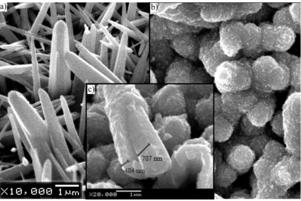
Figure 1 shows different SEM images of the ZnO Nanorod CdTe nanoparticle core-shell arrays. Figure 1(a) shows a bare ZnO NR array before the sensitization stage; is possibly to see the smooth and regular surface of the NR with defined hexagonal crystal habit. In Figure 1(b), (c) ZnO/CdTe NR array are shown, note the smooth surface of the ZnO nanorod in comparison with the rough surface of the CdTe shells. Also, in Figure 1(c) it is also possible to see a detached CdTe shell. Typical measured radius of the NR was about 700 nm and shell thickness of 400 to 450 nm. Moreover, in the centre of Figure 1(c) is clearly visible a ZnO nanorod with the CdTe nanoparticle shell surrounding it.
Figure 1: SEM images of (a) ZnO bare substrate, (b) ZnO/CdTe NR arrays and (c) magnified capture of ZnO/CdTe NR
array.
3.2 Numerical Simulations and Application Range.
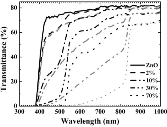
750 (pure ZnO) only one feature is clearly seen. This feature is associated with the ZnO absorption edge located at 3.22 eV (ca. 385 nm). As the content of sensitizer (CdS or CdTe) is increased another feature appears and becomes more noticeable at higher CdS (CdTe) concentration. This new feature is associated with the CdS (CdTe) absorption edge located ca. 2.34 eV for CdS sensitizer and 1.46 eV for CdTe.
Figure 2: Calculated transmittance spectra of simulated ZnO/CdS core-shell array (black curves) and ZnO/CdTe (gray
curves) varying the filling factor for 0 % continuous line, 2 % dashed curve, 10 % dot dashed curve, 30 % double dotted dashed and 70 % dotted curve.
Figure 2 also shows a diminution of the transmittance when increasing fS for both sensitizers. This
diminution represents an absorption enhancement in the spectral region between 400 and 850 nm. For both sensitizers the relative absorption enhancement is larger for small values of fS than for higher fS values.
Moreover, for the same fS changes a smaller enhancement is observed for CdS sensitization than for CdTe.
The simulations correspond with the measurements reproducing the dependencies with the sensitizer content and the appearance of the absorption edges of each material, this confirms that ZnO and sensitizers are spatially apart [6, 8].
However the previous correspondence cannot be used as a way of trying to fit the experimental results due to the validity of the effective medium approximation. In effect, for the correct applicability of the present model the size of the inclusions should be smaller than the wavelength of the light [16]. In fact, for each wavelength there is a large size limit which, depending on the accepted tolerance, would be typically on the order of several tens to more than 100 nm [21], as there are also a small size limit and filling fractions limits. However, beyond these values the effective medium approximation could be used if certain high order corrections are included in eq. (1) [17]. For this reason the present simulation may not be directly used to fit results of the optical properties of the present samples, as the sizes of some of the NR are higher than that (see Fig. 1). But smaller size ZnO NR can be obtained with the use of seed layers for control of their diameter obtaining NR with sizes below that large size limit [22].
Moreover Fig. 1 also shows that there is an empty region (filled with air) between either the bare NR (or the core–shell sensitized ones). Therefore a more complete model should require the introduction of a third phase (air, with unity refraction index) in the effective medium approximation. This will not be considered for reducing the free parameters of the model to just one (i.e., fS with fC= 1 − fS). The empty
751 new parameter related to the porosity should be introduced [23]. Therefore, the choice of the correct solution for the corresponding equation will more complicated [24]. Moreover a graded refraction index or multilayer model would be required, as it is seen in Fig. 1c, the air filling fraction may depend on the sample depth. This dependence would generate a refraction index matching effect already observed in other NR structure [25]. However the study of these effects and similar scattering and light trapping mechanism is beyond the scope of present work.
3.3 Absorption Enhancement
For further study the differences between CdS and CdTe sensitizers in the absorption enhancement, a figure of merit is introduced and calculated. The Solar Irradiance transmitted through these simulated mixtures (IAM1.5T) was calculated from the solar standard total terrestrial irradiance AM 1.5 irradiance spectra (IAM1.50)
and the calculated transmittance (Tj) where j=CdS, CdTe:
0 1.5 1.5 T
AM J AM
I
T
I
(2)In the same way of eq. (2) the irradiance transmitted by the pure ZnO film (fS=0) is defined as
IAM1.5ZnO. Moreover, the total intensity transmitted by the pure ZnO film (P0) and the mixtures (PT) were
calculated from:
P
T=
∫
I
AM1.5 T(
λ
)
d
λ
(3)P
0=
∫
I
ZnOAM1.5(
λ
)
d
λ
(4)And the Figure of merit (F) is defined as:
F
= (
P
0
−
P
T)
P
0 (5)Eq. (5) shows the definition of the figure of merit as the relative difference between the total power (per square meter) transmitted by the ZnO NR film and the total power transmitted by the sensitizer mixture. This quantity is an indicator of the enhancement in the absorption capability of the mixture compared with the capability of absorption of the bare ZnO NR film. Main Figure 3 shows the behaviour of F with fS for
CdS (circles) and CdTe (triangles) sensitizers obtained from simulations. For 0 % sensitizer content both mixtures show 0 % enhancement compared with bare ZnO. As the content of sensitizer starts to increase the absorption of the sensitized mixtures starts to grow from the bare ZnO absorption. Moreover, as fS increases
the figure of merit for the CdTe sensitizer starts to be higher than the one of CdS even for low fS values (i.e. 5
%). Also, a slowing in the increment rate is observed in both sensitizers for fS higher than 40 %. In effect, an
increment from 80 % to 95 % on F is observed for an increase in fS from 40 % to 100 % in the case of CdTe
sensitizer. This saturation like effect on the absorption enhancement indicates an upper threshold for the maximum fS which leads to significant improvements in the absorption of the mixture. Moreover it may have
a crucial significance in the development of solar cells based in these composite structures avoiding unnecessary waste of sensitizer material. Indeed, the incremental power gain for fS higher than 40 % may not
justify the cost of additional sensitizer, leading to savings in needed material in eventual final devices. This saturation like behaviour can be understood due to the exponential dependence of the transmittance with the absorption coefficient , which can be linearized for low absorption. Moreover, for very low sensitizer contents the absorption coefficient depends linearly with fS leading to the almost linear
behaviour observed in Figure 3 (fS < 5 %). As the sensitizer content becomes higher the relation between the
absorption and fS is no more linear. The saturation like effect on the figure of merit is similar to the behaviour
observed for the transmittance when the optical path of the films is increased: the light is mainly absorbed in a region of the order of the penetration depth 1/. Then, this figure of merit is showing an effective enhancement on the optical light path of the samples as the sensitization content is increased.
752 experimental measurements. Although it is difficult to associate the number of cycles with the filling factor this interpretation is still possible because is highly expected that an increase in the number of coatings will provide a greater CdS content in the mixture. Further studies are required to fully understand the nature of the interaction and energy transfer on the ZnO/sensitizer interfaces. However a significant improvement on the photocurrent is observed on the ZnO/CdS NR array compared with the bare ZnO photocurrent [7].
Figure 3: Figure of merit for the absorption enhancement of ZnO/CdS mixtures (circles) and ZnO/CdTe mixtures
(trian-gles). Inset Figure of merit for spin SILAR sensitized ZnO NR CdTe nanoparticles core-shell array.
3.4 Absorption Edge red-shift
In a previous work on previous mentioned spin coating assisted SILAR ZnO/CdS samples a red-shift in the absorption edges positions were reported [6, 8]. Red-shifts between 2.34 eV and 2.66 eV were observed; an increase in the number of cycles generated a red-shift in CdS absorption edge position [6]. Substantially smaller shifts are observed in the simulated mixtures. Therefore, the experimental shifts cannot be explained by the effective medium approximation so different effects (e.g. subbandgap absorption, dispersions and scattering in the surface or nanostructure) could be responsible for the relative large shifts observed [6, 8,26].
753
Figure 4: Diffuse Reflectance spectra of ZnO/CdTe Sample A (dashed) and sample B (dotted). Red and green circles are
the approximated absorption edge positions for CdTe.
Figure 4 shows the diffuse reflectance spectra of two ZnO/CdTe core-shell samples the main difference between them is the electrodeposition potential. For sample A (dashed curve) the potential was -1.1 V while for sample B (dotted curve) was -1.2 V. This different potential values indicate a higher content of CdTe in sample B than the one in sample A [19].
For the analysis, the Kubelka-Munk function (FKM) was calculated from the reflectance spectra (Rdiff). The absorption coefficient was calculated assuming a direct proportionality between FKM and α [27,
28].
2
(1
)
2
diff KMdiff
R
F
R
(6)The main differences between the two spectra are the position of the absorption edges (marked with red and green circles respectively in Figure 4. The positions of the absorption edges were calculated using Tauc plots. This approach is based on linear fits of (α*h )n vs. h plots where n=1/2 for indirect transitions
and n=2 for direct allowed transitions [29]. The procedure used in these calculations was performed following the analysis developed in previous works [6-8, 19, 29].
The low energy (infrared) optical bandgap energy EgL was 1.57 eV and 1.49 eV for samples A and B
respectively. While for the high energy optical bandgap energy EgH the values obtained were 2.55 eV and
2.28 eV for samples A and B respectively. The differences in these values could be associated with the relative higher CdTe content in sample B. Moreover this mayor concentration could be responsible for the high red-shift particularly observed in EgH. As the concentration of CdTe is increased subbandgap absorption
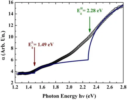
would be more significant compared with the band edge absorption. Moreover as the CdTe NP cover becomes thicker the surface of the NR arrays increase it roughness leading to an augmented light scattering in the NP as previously observed for CdS NP sensitizer [6, 8, 26]. The combination of these effects produces a subestimation in the value of EgH that is clearly observed in Figure 5. Figure 5 shows the experimental
absorption coefficient (circles) plotted with the reconstructed absorption coefficient (continuous curve). The positions of the optical bandgap energies (EgL and EgH) are also marked. The discrepancy between the
non-754 parabolicity of the low lying absorption edge EgL. The reconstructed absorption coefficient was calculated
following the successive absorption edge subtraction procedure developed in previous works [6-8, 20].
Figure 5: Experimental absorption coefficient of sample B (circles) and reconstructed from the absorption band edge
determination absorption coefficient (continuous curve).
The optical bandgap energy obtained from the transmittance measurements (results not shown) were 1.31 eV and 1.36 eV for samples A and B respectively. These energy values, that are lower than the obtained by reflectance, could be explained in terms of the amount of material which interacts with the light beam. Light transmitted through the sample interacts with the full thickness of the sample while reflected light only interact with a thinner one [30]. Then as the interaction with the samples is higher for transmittance measurements a higher red-shift will be observed for transmittance than for the reflectance bandgap energies.
4. CONCLUSIONS
The optical properties of CdS and CdTe sensitized ZnO NR core-shell arrays were studied. An absorption enhancement was observed from numerical simulations and experimental results. This enhancement shows a high grown pace (against sensitizer filling factors) for lower sensitizer content and a smaller one when the concentration is high. Also, saturation like behaviour is observed for both mixtures for filling factors higher than 40 %. This saturation may lead to important sensitizer saving in potential solar cell devices based in these nanostructures. The ZnO/CdTe sensitized mixtures showed the highest rates and also a higher visible absorption than the ZnO/CdS mixtures.
Red-shifts in the bandgap energies were observed as a consequence of the sensitization for ZnO/CdS samples. Also, similar shifts were observed in ZnO/CdTe samples when the same sample was studied by transmittance and reflectance. This is an indicator of the role of dispersions and subbandgap absorption in the bandgap energy position. Both effects are likely to be more significant as the content of sensitizer is increased.
5. ACKNOWLEDGMENTS
CSIC (Comisión Sectorial de Investigación Científica) of the Universidad de la República; Comisión Académica de Posgrados of the Universidad de la República ; ANII (Agencia Nacional de Investigación e Innovación); PEDECIBA–Física, in Uruguay. Junta de Andalucía, Project P07-FQM-02573 in Spain.
6. BIBLIOGRAPHY
114302-755 11, May 2005.
[2] MUSSELMAN, K. P., WISNET, A., IZA, D. C., et al., “Strong Efficiency Improvements in Ultra
-low-Cost Inorganic Nanowire Solar Cells”, Adv. Mater. v. 22, n. 35, pp. E254- E258, Sep. 2010.
[3] OZQÜR, Ü., ALIVOV, Y. I., LIU, V., et al¸ “A comprehensive review of ZnO materials and devices”, J. Appl. Phys. v. 98, n. 041301, pp. 041301-1 – 041301-103 , Feb. 2005.
[4] FAN, Z., RUEBUSCH, D. J., RATHORE, A. A., et al., “Challenges and Prospects of Nanopillar-Based
Solar Cells”, Nano Res. v. 2, n. 829, pp. 829-843, Sep. 2009.
[5] YU, R., LIN, Q., LEUNG, S.-F., et al., “Nanomaterials and nanostructures for efficient light absorption
and photovoltaics”, Nano Energy ,v.1, pp. 57-72, Jan. 2012.
[6] CAMPO, L., PEREYRA, C. J., AMY, L., et al., “Electrochemically Grown ZnO Nanorod Arrays
Decorated with CdS Quantum Dots by Using a Spin-Coating Assisted Successive-Ionic-Layer-Adsorption and Reaction Method for Solar Cell Applications”, ECS J. Solid State Sci. and Technol., v. 2, n. 9, pp.
Q151-Q158, June 2013.
[7] GUERGUERIAN, G., ELHORDOY, F., PEREYRA, et al., “ZnO nanorod/CdS nanocrystal core/shell
-type heterostructures for solar cell applications”, Nanotechnology , v. 22, n. 505401, pp.1-9, Nov. 2011.
[8] PEREYRA, C. J., MAROTTI, R. E., GUERGUERIAN, G., et al., “Optical Properties of
Electrochemically Prepared Zinc Oxide Nanorods”, Energy Environ. Focus, v. 2, n. 4, pp. 257-269, Dec.
2013.
[9] KHAN, Z. R., ZULFEQUAR, M., KHAN, M. S., “Structural, optical, photoluminescence, dielectric and electrical studies of vacuum-evaporated CdTe thin films”, Bull. Matter. Sci. v. 35,n. 2, pp. 169-174, April
2012.
[10] LALITHA, S., KARAZHZNOV, S. ZH., RAVINDRAN, P., et al., “Electronic structure, structural and
optical properties of thermally evaporated CdTe thin films”, Physica B., v. 387, pp. 227-238, Jan. 2007.
[11] AL-DOURI, A. A. J., AL-SHAKILY, F. Y., ALIAS, M. F. A., et al., “Optical Properties of Al- and Sb-Doped CdTe Thin Films,” Advances in Condensed Matter Physics, v. 2010, n. 947684, pp. 1-5, Jan 2010
[12] ADACHI, S., KIMURA, T., SUZUKI, N., “Optical properties of CdTeμ Experiment and modeling”, J. Appl. Phys., v. 74, n. 3435, pp. 3435-3441, Jun. 1993.
[13] PAULSON P. D., MATHEW, X., “Spectroscopic ellipsometry investigation of optical and interface properties of CdTe films deposited on metal foils”, Sol. Ener. Mat. Sol. Cells, v. 82, n. 1, pp. 279-290, May
2004.
[14] NILES, D. W., HÖCHST, H., “Critical test of CdTe(100) angle-resolved photoemission spectra with band-structure calculations”, Phys Rev. B, v. 43 n. 2, pp. 1492-1499, Jan. 1991.
[15] BOJORGE, C. D., KENT, V. R.,TELIZ, E., et al., “Zinc-oxide nanowires electrochemically grown onto
sol–gel spin-coated seed layers”, Phys. Status Solidi A, v.208, n. 7, pp. 1662-1669, July 2011.
[16] STENZEL, O., The Physics of Thin Film Optical Spectra – An Introduction., 1 Ed., Berlin,
Springer-Verlag, 2005.
[17] LIU, Y. C., TUNG, S. K.., HSIEK, J. H., “Influence of annealing on optical properties and surface structure of ZnO thin films”, J. Cryst. Growth. v. 287, n. 1, pp. 105-111, Jan. 2006.
[18] NIMONIYA, S., ADACHI, S., “Optical properties of wurtzite CdS ”, J. Appl. Phys. v. 78, pp.
1183-1190, March 1995.
[19] NICHELATTI, E., “Complex refractive index of a slab from reflectance and transmittanceμ analytical solution”, J. Opt. A: Pure Appl. Opt., v. 4, pp.400-403, May 2002.
[20] GUERGUERIAN, G., ELHORDOY, F., PEREYRA C. J., “ZnO/Cu2O heterostructure nanopillar arraysμ synthesis, structural and optical properties”, J. Phys. D: Appl. Phys. v. 45, n. 245301, pp. 1-10, May
2012.
[21] NIKLASSON G. A., GRANQVIST, C. G., HUNDERI, O. “Effective médium model for the optical properties of inhomogeneous materials”, Appl. Opt., v. 22, n.1, pp. 26-30, 1981
[22] BOJORGE, C. D.; KENT, V. R., TELIZ, E., et al.,“Zinc Oxide Nanowires Electrochemically Grown
onto Sol-Gel Spin Coated Seed Layers”, Physica Status Solidi A, v. 208, n.7, pp.1662–1669, 2011
(doi:10.1002/pssa.201026752)
[23] PEREYRA, C. J., MAROTTI, R. E., GUERGUERIAN, G., et al.,“Optical Properties of Sensitized Zinc
Oxide Nanorods Electrochemically Prepared”, Energy and Environment Focus, v.2, n.4, pp.257-269, 2013.
756 [24] DAVOINE, F. ., GALIONE, P. A., RAMOS-BARRADO, J. R., et al.,“Modeling of gradient index solar
selective surfaces for solar thermal applications”, Solar Energy, v. 91, pp. 316-326, 2013. (DOI:
10.1016/j.solener.2012.09.019)
[25] BADÁN, J. A., MAROTTI, R. E., DALCHIELE, E. A., et al.,“Optical Properties of Si Nanowires:
Dependence with Substrate Crystallographic Orientation and Light Polarization”, Journal of Materials Research, doi 10.1557/jmr.2015.47
[26] RABINOVICH, E., HODES, G., “Effective Bandgap Lowering of CdS Deposited by Successive Ionic Layer Adsorption and Reaction”, J. Phys. Chem. C., v. 117, n. 4, pp. 1611-1620, Jan. 2013.
[27] TORRENT, J., BARRÓN, V., Encyclopedia of Surface and Colloid Science, edited by Hubbard, A. T., 2
ed., New York, CRC Press, 2002.
[28] SCHRÖDERAND, U., SCHOLZ, F., “Microscopic in situ diffuse reflectance spectroelectrochemistry of solid state electrochemical reactions of particles immobilized on electrodes”, J. Solid State Electrochem. v. 1,
n. 1, pp.62-67, July 1997.
[29] KIM, E., JIANG, Z.T., NO, K., “Measurement and calculation of optical band gap of chromium aluminum oxide films”,J. Appl. Phys., v.39, n.8, 2000.
[30] JOHNSON, S. R., TIEDJE, T., “Temperature Dependence of the Urbach edge in GaAs”, J. Appl. Phys.