Abstract—A practical procedure to reduce the back lobe level of linear microstrip antenna arrays is presented in this paper. The novel concept consists in the design of the radiators asymmetrically positioned with respect to the ground plane. In order to validate this technique, a four-element linearly-polarized array is designed in the HFSS software and a prototype is manufactured. Furthermore, the design of beamforming circuit to achieve broadside radiation and -20 dB side lobe level is detailed. Very good agreement between simulated and experimental results is obtained. Although the technique is presented for linearly polarized arrays, it is general and can also be applied in the circularly polarized ones.
Index Terms— microstrip antenna arrays, beamforming circuit, back lobe
suppression
I. INTRODUCTION
Microstrip antenna arrays are widely used in global navigation satellite systems (GNSS) and
communication systems due to its low profile characteristic, conformability, lightweight and low cost
[1]. These arrays, when composed by linearly polarized patches in side by side configuration [2],
exhibit a high back lobe level [2]-[4] due to asymmetric E-plane radiation pattern [5]. This undesired
behavior allows that multipath signal propagation remain a dominant cause of error in differential
positioning system [6]. Also, it affects the coverage capacity of base station sectorial antenna, due to
the overlapping areas between adjacent sectors [7].
The above-mentioned difficulties can be mitigated by using a low back lobe antenna. In the case of
base station antennas array, FBR (front-back ratio) more than 20 dB is recommended in order to
increase the subscriber capacity [7]. Various solutions for the improvement of FBR performance are
available in the literature [6]-[14]. These solutions, based on technologies like that: electromagnetic
bandgap (EBG), micromachining technology, substrate integrated waveguide (SIW), slotted ground
choke, leaky-wave antenna, ground plane edge shaping and backed reflector behind the radiator, are
efficient, but make manufacturing process more complex. The improvement of the FBR in a simple
way is proposed in this paper, the solution is based on the antennas positioning with respect to the
ground plane, thus making the manufacturing process simpler. This paper is structured as follow: In
Design of Microstrip Antenna Array with
Suppressed Back Lobe
Eduardo S. Silveira, Daniel C. Nascimento, Alexis F. Tinoco-S.
Laboratory of Antennas and Propagation, Technological Institute of Aeronautics, São José dos Campos – SP, Brazil. E-mails: [email protected], [email protected], [email protected]
Marcus V. P. Pina
the section II the back lobe radiation of a probe fed linear microstrip antenna array is presented as
result of the asymmetric far field E-plane radiation pattern. In the sequence a technique based on the
antenna positioning with respect of ground plane is carried out, reducing the undesired back lobe. This
technique applied to a side by side array that makes the E-plane far field symmetric is assisted by a
parametric simulation.
Section III describes a four-element side by side array design based on the prior studies. Special
attention is given to the beamforming circuit design in section IV, to synthetize the excitation
coefficients for a side lobe level of -20 dB. The section V shows the array prototype manufacturing
and its experimental input impedance matching and radiation characteristics, compared with the
theoretical ones. According [7] a FBR better than 20 dB is the goal of this work.
II. BACK LOBE ANALYSIS
Before starting the finite ground plane array design, a study of back lobe radiation becomes
necessary for the better understanding of the back radiation mechanism. This undesired effect is
treated in this work by the analysis of single antenna and two arrays printed in dielectric substrate of
2.55 relative permittivity and 3.048 mm thickness, both designed in HFSS software.
Firstly, a linearly-polarized single microstrip radiator is analyzed in HFSS software to elucidate the
E-Plane asymmetries effect [5] and to provide elementary knowledge and skills for the array design.
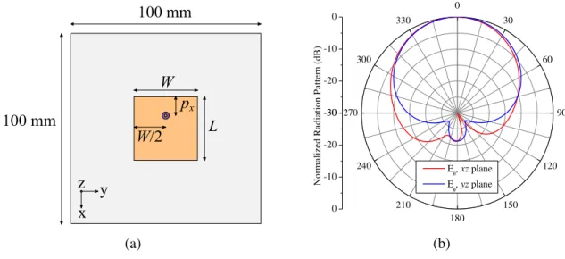
The analyzed antenna operating at 2.5 GHz (Fig. 1a) is a probe fed square microstrip patch of
dimensions (35.0 mm×35.0 mm), printed atop of square dielectric substrate of dimensions (100.0 mm
× 100.0 mm). Radiation patterns of E-plane (xz), and H-plane (yz), are presented in (Fig. 1b). The
radiator operates in the fundamental mode (TM10z ), taking the Fig. 1(a) as reference.
(a)
-30 -20 -10 0
0
30
60
90
120
150 180
210 240 270
300 330
-30
-20
-10
0
N
o
rm
a
li
z
e
d
R
a
d
ia
ti
o
n
P
a
tt
e
rn
(
d
B
)
Exz plane
Eyz plane
(b)
Fig. 1. (a) Single element microstrip antenna and its (b) E- and H-plane radiation patterns.
The E-plane radiation pattern of this radiator is indubitably asymmetric, enforcing a relevant field
level in the back region. The asymmetric far field is attributable to the difference in phase between the
contributes to radiation pattern distortion [15]. This asymmetric shape in the E-plane is more
pronounced for antennas printed in thicker substrates [16].
This undesired far field in the back region of a single element will create a high back lobe level
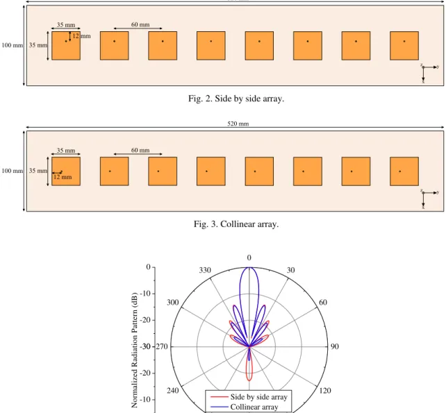
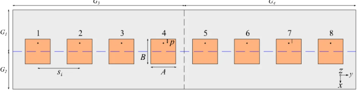
when an array is composed. The back lobe behavior is next investigated in terms of the eight-elements
arrays with half-wavelength spacing, in the side by side (Fig. 2) and collinear (Fig. 3) configurations.
These arrays are designed in HFSS software and uniformly excited. Radiation pattern for both
configurations are presented in Fig. 4. This figure illustrates that back lobe of side by side
configuration is higher than collinear one. Depending on the electrical dimensions of ground plane
and substrate thickness, the back lobe grows to unacceptable values [2], [16]-[17].
Fig. 2. Side by side array.
Fig. 3. Collinear array.
-30 -20 -10 0
0
30
60
90
120
150 180
210 240 270
300 330
-30
-20
-10
0
N
o
rm
a
li
z
e
d
R
a
d
ia
ti
o
n
P
a
tt
e
rn
(
d
B
)
Side by side array Collinear array
Fig. 4. Radiation pattern of uniformly excited arrays – yz plane.
An intuitive way to reduce the back lobe of side by side array is the compensation of fringing phase
differences, making the E-plane radiation pattern symmetric and with a null at back lobe direction. In
radiators asymmetrically positioned with respect to the ground plane.
In order to get this condition, a back lobe level is investigated by a parametric analysis of relative
positioning of the radiators with respect of the ground plane. This analysis is carried out, looking for
the null of back lobe level that is achieved when the diffracted fields at ground plane border reach a
condition that compensates the difference of the fringes phase.
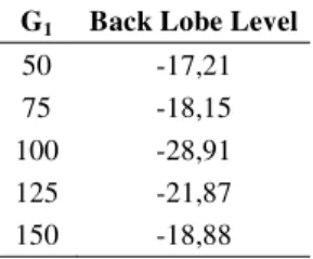
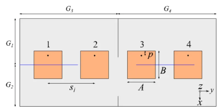
The relative positioning of radiators above ground plane is established by variables (G1, G2, G3, and
G4), in accordance with the dashed black and blue symmetry lines defined in the Fig. 5. Given the
ground plane asymmetry variables, a parametric study was carried out and its results are shown as
follows. During this study, each parameter was varied alone, while the rest were held fixed. The
standard values for the parameters are: G1 = G2 = 50 mm and G3 = G4 = 260 mm. The influence of the
variables G1 and G2 in the antenna array radiation pattern is shown in Fig. 6.
Fig. 5. Antenna array geometry.
-30 -20 -10 0 0 30 60 90 120 150 180 210 240 270 300 330 -30 -20 -10 0
G1 = 50 mm G1 = 75 mm G1 = 100 mm G1 = 125 mm G1 = 150 mm
N o rm al iz ed R ad ia ti o n P at te rn ( d B ) (a) -30 -20 -10 0 0 30 60 90 120 150 180 210 240 270 300 330 -30 -20 -10 0 G 2 = 50 mm G2 = 75 mm G2 = 100 mm G
2 = 125 mm G2 = 150 mm
N o rm a li z e d R a d ia ti o n P a tt e rn ( d B ) (b)
Fig. 6. Antenna array total electric field for (a) G1 and (b) G2 variations –ϕ = 90º plane.
From the parametric analysis it is clear that setting correctly G1 and G2 dimensions, the back lobe
can be suppressed. To make evident the back lobe level reduction, the Tables 1 and 2 were built,
synthetizing the data from the radiation patterns showed in Fig. 3 (a) and (b). On the other hand, in
Fig. 7, the influence of G3 and G4 parameters, in the array back lobe is presented. One can observe
TABLE I. VARIATION OF THE BACK LOBE LEVEL (dB) WITH G1(mm). G1 Back Lobe Level
50 -17,21 75 -18,15 100 -28,91 125 -21,87 150 -18,88
TABLE II. VARIATION OF THE BACK LOBE LEVEL (dB) WITH G2(mm). G2 Back Lobe Level
50 -17,21 75 -18,05 100 -24,20 125 -19,68 150 -17,85
-30 -20 -10 0 0 30 60 90 120 150 180 210 240 270 300 330 -30 -20 -10 0
G3 = 260 mm G
3 = 272,5 mm G
3 = 285 mm G3 = 297,5 mm G3 = 310,0 mm
N o rm a li z e d R a d ia ti o n P a tt e rn ( d B ) (a) -30 -20 -10 0 0 30 60 90 120 150 180 210 240 270 300 330 -30 -20 -10 0 G 4 = 260 mm G4 = 272,5 mm G4 = 285 mm G
4 = 297,5 mm G4 = 310 mm
N o rm a li z e d R a d ia ti o n P a tt e rn ( d B ) (b)
Fig. 7. Antenna array total electric field for (a) G3 and (b) G4 variations –ϕ = 90º plane.
III. ARRAY DESIGN
After detailing the back lobe level control process, the design of a four-elements array with
half-wavelength spacing assisted by HFSS software is carried out, which allows a prototype to be built and
tested. The array geometry is presented in Fig. 8. Using the Arlon CuClad 250-GX of 3.048 mm
thickness, the array patches dimensions (A=B=35 mm) are established to provide an ISM 2.5 GHz
operating frequency. The probe position p is set to 12 mm. The separation Si between the elements is
defined as 60 mm (λ0/2). As previously exposed, the ground plane dimensions are (G1 = 100 mm, G2
= 50 mm, and G3 = G4 = 140 mm), to eliminate the back radiation. The antennas are excited with the
following incident voltage wave coefficients [18] (a1 = a4 = 0.64 and a2 = a3 = 1), calculated by a least
square linear constraints algorithm [19], establishing SLL (side lobe level) of -20 dB. The coefficients
indexes are related to each array element, taking the Fig. 8 as reference. To illustrate the potential of
mm and G2 = 50 mm) and symmetric (G1 = G2) ground plane are shown in Fig. 9.
Fig. 8. Antenna array geometry.
-30 -20 -10 0
0
30
60
90
120
150 180
210 240 270
300 330
-30
-20
-10
0
N
o
rm
a
li
z
e
d
R
a
d
ia
ti
o
n
P
a
tt
e
rn
(
d
B
)
Asymmetrical ground plane Symmetrical ground plane
Fig. 9. Antenna array radiation patterns for symmetrical and asymmetrical ground planes –ϕ = 90º plane.
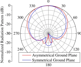
Finally, to validate the explanation above described with respect of asymmetric radiation pattern,
the far field E-plane (xz-plane) of the array is plotted in Fig. 10 for the asymmetrical and symmetrical
ground plane conditions. Using the correct asymmetrical ground plane dimensions, it is possible to
observe the symmetric radiation pattern with a null at θ = 180o, responsible for the back lobe
elimination. After the array project, the next step consists in the beamforming circuit design,
-30 -20 -10 0
0
30
60
90
120
150 180
210 240 270
300 330
-30
-20
-10
0
N
o
rm
a
li
z
e
d
R
a
d
ia
ti
o
n
P
a
tt
e
rn
(
d
B
)
Asymmetrical Ground Plane Symmetrical Ground Plane
Fig. 10. Antenna array radiation patterns for symmetrical and asymmetrical ground planes –ϕ = 0º plane. IV. BEAMFORMING CIRCUIT DESIGN
The topology of the antenna array with beamforming circuit is a multilayer structure presented in
the Fig. 11, where the circuit is positioned behind the antenna ground plane. The beamforming
dielectric substrate is the TMM 4 of h2 = 0.381 mm. An electrical thin substrate is employed in order
to reduce microstrip circuit radiation. Note that, due to relative permittivity and dielectric thickness,
the employed microstrip transmission line characteristic impedance (Z0) is extremely low (values
between 20 Ω and 50 Ω). This values are used to insure widths between 0.7 mm and 2.6 mm to
designed transmission lines.
Fig. 11. The cross section of the array topology.
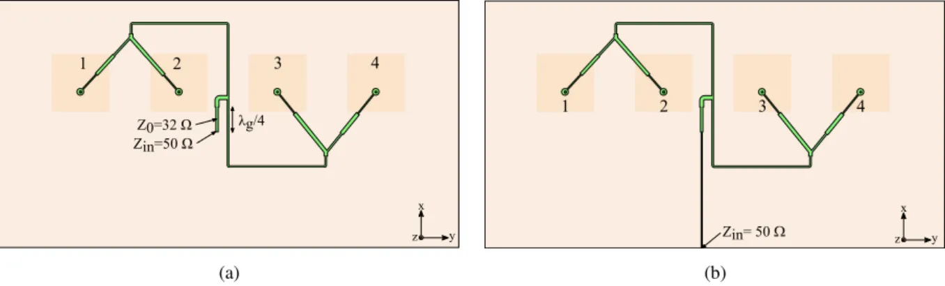
Having chosen the beamforming structure, the transition between the printed antenna and the
beamforming circuit was designed following [2]. It is composed of a cylindrical probe (radius = 0.65
mm and length = 3.429 mm). Firstly, considering the aforementioned coefficients, the beamforming
circuit was optimized for real active input impedance (Zin) at the reference planes (RP) indicated in
Fig. 12 (a). Furthermore, in Fig. 12 (b), the first set of quarter wave transformers are used to reduce
(a) (b)
Fig. 12. Definition of (a) reference planes (RPs) impedances and (b) first set of quarter wave transformers.
Next, a second set of quarter wave transformers are designed (see Fig. 13 (a)) to make physically
possible the implementation of the T-junctions. The impedances of this second set of transformers were designed to provide the desired excitation coefficients, and to impose a 40-Ω of input impedance at the T-junctions as shown in Fig. 13 (b).
(a) (b)
Fig. 13. (a) Second set of quarter wave transformers and (b) connection of the terminals in T junctions.
The T-junctions input terminals were then extended by means of matched microstrip lines (40 Ω), as it is shown in Fig. 14 (a). Then, a novel T-junction was introduced to connect the two circuit
sections, as it can be seen in Fig. 14 (b).
(a) (b)
Finally, the input terminal of the final T junction has its input impedance transformed to 50 Ω by a 32-Ω quarter wave transformer (see Fig. 15 (a)). A 50-Ω microstrip line is then used to extend the terminal connection up until the array edge (Fig. 15 (b)), allowing the inclusion of a SMA connector.
(a) (b)
Fig. 15. (a) Inclusion of a final quarter wave transformer and (b) insertion of a 50-Ω microstrip line.
V. ARRAY PROTOTYPE AND EXPERIMENTAL RESULTS
After the array (section III) and beamforming circuit (section IV) designs, a prototype was
manufactured on LAP/ITA (Laboratory of Antennas and Propagation of Technological Institute of
Aeronautics). The antenna array and beamforming circuit were manufactured using the T-Tech Quick
Circuit AMC 2500. These two dielectric substrates were integrated using the Rogers 3001 bonding
film. As this bonding film is a low loss dielectric, the antenna array ground plane had to be removed,
imposing that the beamforming circuit ground plane works like antennas array ground plane
simultaneously.
The beamforming circuit prototyped in the TMM substrate is presented in Fig. 16 (a) whereas the
antenna array prototyped in the Arlon CuClad is presented in Fig. 16 (b). Note that, a copper-made bar was introduced in the structure (see Fig. 16 (b)), providing mechanical support to the 50-Ω SMA connector. Simulations of the array in the presence of this metallic support were carried out indicating
that array works properly as previously expected.
(a) (b)
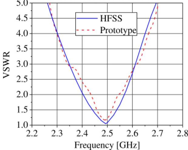
The experimental VSWR (Voltage Standing Wave Ratio) from measurements with a VNA (Vector
Network Analyzer) Agilent N5230A and the simulated one with HFSS are shown in Fig. 17. To
conclude the analysis, the experimental and simulated radiation patterns in zy-plane are compared.
The measurements were carried out in the anechoic chamber located at LIT-INPE (Integration and
Testing Laboratory – Brazilian Institute of Space Research). The results for the zy-plane patterns are
presented in Fig. 17 and show that SLL and back radiation are properly controlled under -20 dB, as
specified. From these figures, it is found that theoretical and experimental results are in very good
agreement.
2.2 2.3 2.4 2.5 2.6 2.7 2.8
1.0 1.5 2.0 2.5 3.0 3.5 4.0 4.5 5.0
V
S
W
R
Frequency [GHz] HFSS Prototype
Fig. 17. VSWR of linearly polarized array.
-30 -20 -10 0
0
30
60
90
120
150 180
210 240 270
300 330
-30
-20
-10
0
N
o
rm
a
li
z
e
d
R
a
d
ia
ti
o
n
P
a
tt
e
rn
(
d
B
)
HFSS Prototype
Fig. 18. Experimental and simulated normalized radiation patterns.
VI. CONCLUSION
This paper has shown a simple and easy-to-manufacture concept to reduce the back lobe level of
microstrip antenna arrays. The proposed procedure is based on the asymmetrical disposal of the array
elements with respect to the ground plane. A four-element linearly polarized antenna array was
designed to verify the concept and special attention to its beamforming circuit design was given.
Details about the beamforming circuit synthesis based on the active input impedance optimization
were provided in a step-by-step approach. The FBR and SLL better than -20 dB was achieved in the
between prototype and theoretical results are certainly due to the inaccuracies in the construction
processes, since it involves the bonding of the two substrates.
ACKNOWLEDGMENT
The authors would like to thank LIT/INPE for providing the use of the anechoic chamber and the
Brazilian National Council for Scientific and Technological Development – CNPq, for the financial
support of the projects 402017/2013-7, 131459/2014-7, and 141103/2016-7.
REFERENCES
[1] R. Garg, P. Bhartia, I. Bahl, A. Ittipiboon: “Microstrip Antenna Design Handbook”, Norwood, MA: Artech House, 2001. [2] D. C. Nascimento, J. C. da S. Lacava: “Design of Arrays of Linearly Polarized Patch Antennas on an FR4 Substrate: Design of a probe-fed electrically equivalent microstrip radiator”, IEEE Antennas and Propagation Magazine, vol. 57, no. 4, pp. 12-22, 2015.
[3] Y. M. Yoon, J. H. Kim, B. G Kim: “Radiation characteristics of an H-plane linear microstrip array antenna on a finite substrate”, 2013 IEEE Antennas and Propagation Society International Symposium (APSURSI), 2013.
[4] S. Farzaneh, A. R. Sebak: “Microwave Sampling Beamformer – Prototype Verification and Switch Design”, IEEE Trans. Microwave Theory and Techniques, vol. 57, no. 1, pp. 36-44, Jan. 2009.
[5] T. Namiki, Y. Murayama, K. Ito: “Improving radiation-pattern distortion of a patch antenna having a finite ground plane”, IEEE Trans. Antennas Propagat., vol. 51, no. 3, pp. 478-482, 2003.
[6] W.-G. Lim, H.-s Jang, J.-W. Yu: “New Method for Back Lobe Suppression of Microstrip Patch Antenna for GPS”, Proceedings of the 40th European Microwave Conference, Paris, France, September, 2010.
[7] Y. Rikuta, H. Arai, Y. Ebine: “Enhancement of FB Ratio for Cellular Base Station Antenna by Optimizing Reflector Shape”, IEEE Antennas and Propagation Society International Symposium, Boston, USA, July, 2001, pp. 456-459, doi 10.1109/APS.2001.960133.
[8] L. Zhang, S. Gao, Q. Luo, P. R. Young, Q. Li, Y.-L Geng, R. A Abd-Alhameed: “Single-Feed Ultra-Wideband Circularly Polarized Antenna With Enhanced Front-to-Back Ratio”, IEEE Trans. Antennas Propag., vol. 64, no. 1, pp. 335-360, Jan. 2016.
[9] T. J. Cho, H. M. Lee: “Front-to-Back Ratio Improvement of a Microstrip Patch Antenna by Ground Plane Edge
Shaping”, 2010 IEEE Antennas and Propagation Society International Symposium, Toronto, ON, July, 2010, pp. 1-4, doi 10.1109/APS.2010.5561174.
[10]H.-m. Lee, J.-k. Kim: “Front-to-Back Ratio Improvement of a Microstrip Patch Antenna using an Isolated Soft Surface Structure”, Proc. of the 39th European Microwave Conference, Rome, Italy, September, 2009.
[11]Y.-L. Chiou, J.-W. Wu, J.-H. Huang, C. F. Jou,: “Design of Short Microstrip Leaky-Wave Antenna With Suppressed Back Lobe and Increased Frequency Scanning Region”, IEEE Trans. Antennas Propag., vol. 57, no. 10, pp. 3329-3333, Oct. 2009.
[12]J. Wei, Z. N. Chen, X. Qing, J. Shi, J. Xu,: “Compact Substrate Integrated Waveguide Slot Antenna Array With Low Back Lobe”, IEEE Antennas Wireless Propag. Lett., vol. 12, 2013.
[13]M. Karami, R. A. Sadeghzadeh, M. Noferesti, M. Chegeni: “Suppressed back-lobe substrate-integrated waveguide slot array antenna for X-band”, IET Electron. Lett., vol. 51, no. 11, pp. 811-813, May 2015.
[14]Z. Aijaz, S. C. Shrivastava: “Techniques to Reduce the Back Lobe of Microstrip Slot Antenna”, International Journal of Electronic Engineering Research, vol. 2, no.1, pp. 15-22, 2010.
[15]Ribeiro Filho, P. et al. “Probe-fed hybrid-patch cylindrical SIW antenna”. 2014 IEEE Antennas and Propagation Society International Symposium (APSURSI), 2014.
[16]D.C. Nascimento. “Thick-substrate microstrip antenna arrays with beamsteering, side lobe level and directivity control”. D. Sc. Thesis. Instituto Tecnológico de Aeronáutica, São José dos Campos, Brazil, 2013. (in Portuguese).
[17] M. Bonadiman. “Microstrip antenna array for airborne synthetic aperture radar”. M. Sc. Thesis. Instituto Tecnológico de Aeronáutica, São José dos Campos, Brazil, 2004. (in Portuguese).
[18]D. M. Pozar: “The active element pattern”: IEEE Transactions on Antennas And Propagation , v. 42, n. 8, p. 1176-1178, 1994.