Abstract—An attempt has been made to present a new device which
will function as a highly efficient SDR (Single Drift Region) P+-N-N+ IMPATT diode utilizing the advantages of a junctionless field effect transistor. The basic idea is to convert a uniform N+ region into a (P+–N–N+) structure without any requirement of physical doping. As the present device works on the principle of a junctionless channel, variability and short channel effects are significantly reduced as compared to the conventional TFET though the requirement of an extra gate increases a few fabrication steps. Further, efficiency more than conventional SDR IMPATT diode is achievable without any physical doping.
Index Terms—ControlGate, efficiency, electric field, IMPATT, P-gate, SDR.
I. INTRODUCTION
The IMPATT (IMPact-Avalanche-Transit Time) diode is a popular transit time device which gains
its reputation in microwave (3-30 GHz) and millimeter wave (30-300 GHz) digital and analog
communication systems as well as in radar for civilian purposes and for defense systems in missiles.
In order to produce negative resistance at microwave frequencies, these diodes utilize impact
ionization and transit time properties of semiconductor structures. Impact ionization is a process of
formation of additional holes and electrons by knocking them out of the crystal structure due to high
electrons and holes velocity. In IMPATT devices, negative resistances arise from two delays
(avalanche delay-caused by finite build-up time of avalanche current, transit time delay- caused by the
finite time taken by the carriers to cross the drift region) which cause the current to lag behind voltage
[1]. These two delays add up to 1800 phase lag at a particular frequency and so the diode resistance is negative corresponding to that frequency.
On the other hand, it is observed that the characteristics of a nano-scale Metal Oxide Semiconductor
Field Effect Transistors (MOSFET) have deteriorated owing to continual down scaling in size. Due to
continual reduction in the dimensions of the MOS devices, various short channel effects (SCEs) such
as Drain Induced Barrier Lowering(DIBL), gate tunneling, punch through, surface scattering etc are
very much predominant along with several severe fabrication issues (especially in the sub-20nm
channel region). So continuous efforts have been made in the recent years to improve the SCE
immunity by using single as well as dual material double gate SOI/SON MOSFET structures [2-5].
A JL-SDR-IMPATT Device with Improved
Efficiency
Dipan Bandyopadhyay, Subir Kumar Sarkar.
However, these severe issues especially that of fabrications have been reduced by junctionless tunnel
Field effect Transistor (absence of physical p-n junction in the source or drain side) where only a
uniformly doped channel has been present [6-11].This structure produces excellent immunity to SCEs
(Short Channel Effects) and double-gate or multi-gate devices offer better scalability options. Besides,
this device is simpler to fabricate and has less variability and better electrical properties than
MOSFET. So, these attractive advantages of the junctionless TFETs encourage us to use this kind of
devices as junctionless SDR IMPATT device.
At different millimeter-wave window frequencies, Si and GaAs IMPATTs are already established
as efficient and powerful sources [12-14]. For generation of RF power at THz frequencies, the
potentiality of wide band-gap materials (GaN,SiC) has been reported in the recent years. Though
different semiconductor materials like GaAs, InP, GaN have been used for IMPATT development to
achieve higher efficiency, power output and frequency range, silicon still remains the most reliable
material for millimeter-wave IMPATTs owing to its advanced technology and stability. The device
efficiency of a silicon SDR (p+-n-n+) IMPATT diode at Ka-band is found to be 7.84%-8.98%. The
maximum efficiency observed for 4H-SiC SDR IMPATT diodes is 23.28% (for Ka band)
[15-17].Since this efficiency is quite low, continuous efforts have been made in the recent years to
increase the efficiency.
In this paper, an attempt has been made to present a new device which will function as a highly
efficient SDR (Single Drift Region) P+-N-N+ IMPATT diode utilizing the concept of a junctionless
field effect transistor. The basic idea is to convert a uniform N+ region into a (P+–N–N+) structure
without any requirement of physical doping. Since this device is based on the principle of a
junctionless channel, variability and short channel effects immunity improves as compared to the
conventional TFET though the requirement of an extra gate increases a few fabrication steps. Besides
without any physical doping greater efficiency can be achieved than that of a normal SDR IMPATT
diode.
II. DEVICEDESCRIPTION
The proposed device structure is a lateral n+-type JLFET which uses two isolated gates (Control Gate
and P-gate) of two different metal work functions, to make the layer beneath the gates n-type and
p+-type. We have chosen the metal work function as 4.27 eV and 5.93eV for the CG and PG electrode, to
make the layer beneath the CG and the PG electrode n-type and p+-type respectively [18-19]. As soon
as the contact is made between metal oxide and the N+ semiconductor, the electrons will flow from
the semiconductor to the metal and thus Fermi level goes down and in equilibrium this level is aligned
with the Fermi level of the metal. For higher metal work function, more and more electron flow from
the semiconductor to the metal and the Fermi level goes down more towards the valence band. In this
way, a N+ region can be converted to N and P+ region depending on the metal work function .The
Fig.1. The device structure indicating the N+ ,N and P+ regions along with the Control gate and P gate where two different metals( indicated by blue and green) and oxide layers(indicated by yellow).
Fig.2. The approximate energy band diagram for the N+, N and P+ regions
III. ANALYTICALMODELOFELECTRICFIELDANDEFFICIENCY
Considering n+ degenerate type semiconductor bar, the position of the Fermi level for this degenerate
semiconductor can be written as [20]
3 -n+ 2 n+ Fn+ c
c c
n n
E = E + kT[ln( )+ 2 ( )]
N N (1) where Ncis the carrier density in the conduction band, k is the Boltzmann’s constant,Tis the
temperature in Kelvin, nn+is the carrier concentration in the n+ bar and Ecis the conduction band energy
The position of the Fermi level for a n- type region can be written as
n-Fn- c
c n E = E + kT[ln( )]
N (2) where nn--the carrier concentration in the n region
Solving equations (1) and (2) we get,
3 -n- 2 n+ Fn- Fn+
n+ c
n n
E = E + kT[ln( ) - 2 ( )]
n N (3)
Again, the position of the Fermi level for a p+ degenerate type region can be written as
3 -p+ 2 p+ Fp+ v
v v
p p
E = E - kT[ln( )+ 2 ( )]
N N (4)
3
-p+ n+ 2 n+ p+ Fp+ Fn+ g
c v c v
p n n p
E = E - E - kT[ln( ) - 2 ( + )]
N N N N (5)
The metal work functions for the Control gate and the P-gate can be expressed as
Fn+ Fn-MC sn+
E - E
= +( )
q
(6)
Fn+ Fp+ MP sn+
E - E
= +( )
q
(7)
whereMC MP-the metal work functions for the Control Gate and the P-gate andsn -the
semiconductor work function
Solving the above equations we get,
Fp+ Fn-MC MP
E - E
= +( )
q
(8)
The conditions for converting the N+ region to intrinsic-type, n-type and p+-regions
are g
min min g min
E
ΔE = - 3kT,ΔE < ΔE ,E -6kT > ΔE > ΔE
2 and ΔE > E - 6kTg
Now, from the 2D-Poisson’s equation, the electrostatic potential profile can be written as
2 2 D 2 2 si qN ψ ψ + = x y
(9)
where ND is the donor concentration in the n region of the device,qis the electronic charge and si is the silicon substrate permittivity.
An approximate solution of the 2D potential distribution can be proposed assuming a parabolic
potential as suggested by Young [21]
ψ(x, y)= ψ (x)+a (x)y+a (x)ys 1 2 2 (10) wheres( )x -the surface potential which varies along the channel a1, a2are functions of x.Now,
introduction of symmetric conditions with respect to tsi
2 [22] leads to 2 1 s 1 si a (x)y
ψ(x, y)= ψ (x)+ a (x)y
-t
(11) where tsi-the substrate thickness
With the introduction of boundary conditions at the surface i.e. y=0
ψ(x, y) =
y i s gp ox si ox
(ψ (x)-V )
t
,we then
derived an expression for a x1( )
i s gp ox y=0 1 si ox
(ψ (x)-V )
ψ(x,y)
= a (x) =
y t
(12) where i gp MS
gp
V = V - and tox-the oxide thickness
Substituting the value of a x1( ) from equation (12) to (11) we get,
i 2
gp
ox ox ox
s
si ox si ox si si ox si
V
y y y
ψ(x,y)= ψ (x)[1+ - ] + [ -1]
t t t t t
(13) Now, substituting the above expression of ψ(x, y) in (9), a new differential equation in terms of the
surface potential is obtained as
i 2
ox gp
s ox s D
2
si ox si si ox si si
2 V
ψ 2 ψ (x) qN
- + =
t t t t
x
Let ox si ox si 2 M =
t t , i
D gp si qN
P - MV
Therefore, the equation (14) simplifies to
2
s
s 2
ψ (x)- Mψ (x)= P
x
(15)
Solving the differential equation of (7) we get
x - x
s
P
ψ (x)= Ae + Be
-M (16) where = ε
Now, the boundary conditions-
s s si bi
ψ (0,0)= ψ (0,t )=V ,ψ (δ,0)= ψ (δ,t )= V +Vs s si bi n p have been used to solve for the constants A and B
δ
bi bi n p
δ - δ δ
-δ
bi bi n p
δ - δ
bi
P P
(V + )e - (V +V + )
M M
B =
e - e
e P P
= ( )[(V + ) - (V +V + )e ]
M M
e - e
P
A = V + - B
M
whereVn p -the applied voltage across the p+ and n+ regions,Vbi- built-in potential
Now the expression of electric field can be obtained from differentiating the equation (16),
x - x
s
E (x) = [Ae - Be ] (17)
Now, if an ac voltage vVmaxsinwtis superimposed on applied dc voltage V = Vr n p , the efficiency of the device is given by [23]
max B
2V Efficiency(η)=
πV (18) whereVBis the breakdown voltage and is given by
V = xB Aξ +(W - x )ξA A D (19) whereA ,Dare electric field in the avalanche and the drift region and xA,W are the avalanche width
and depletion width where the electric field decays to zero.
The maximum ac voltage depends on swing in the electric field in the avalanche and drift region
max
V =ΔξW
Considering optimistic situation i.e. the voltage across the drift zone swings to zero thereby making
the electric field zero at the maximum negative voltage of the ac voltage i.e.Δξ = ξDand the with the
assumption that ξ = 2ξA D,the efficiency can be modified as [23]
A 2 1 η = x π1+ W (20)
The avalanche width (xA) can be derived from the equation (17) as
max
A 2
E
[ - (A- B)]
2 x =
(A+ B) (21)
The depletion width on the other hand can also be derived from the equation (17) by setting the
electric field as zero
ln(B / A) W =
2 (22) IV. RESULTSANDDISCUSSION
In this section, variations of electric field with the length along the drift region for different
parameters, efficiency variations with carrier concentration, oxide permittivity and oxide thickness
have been studied. Besides efficiency comparison has been made for the junctionless SDR IMPATT
and conventional SDR IMPATT. Fig. 3 depicts the variation of the electric field with length along the
drift region for two different biasing voltages of 0.5 V and 0.35 V (equivalent electric fields of more
than 10 *10 7 V/m), applied across the device i.e. between P+ and N+ regions. For an applied bias of 0.5 V and 0.35 V, the electric field is maximum at the P+-N junction as expected where avalanche
breakdown occurs. It is to be noted that in silicon avalanche breakdown occurs at a field of ~5 *10 7 V/m- for carrier concentration of 1023/m3 which we have used in our calculations[24]. It is thus established the occurrence of impact ionization at a biasing voltages of 0.5V and 0.35 V. The electric
field decreases as we proceed along the drift region. Eventually it decreases to a value close to zero
near the n+ region. Another significant observation is that the electric field decreases comparatively
faster as the voltage, applied across the device is increased as with the increase of reverse bias, more
and more electrons immobile acceptors are created in the N+ region and therefore the electric field
decreases more rapidly at a higher reverse bias. It is depicted in Fig.4 that the electric field profile of
the junctionless SDR IMPATT almost resembles that of a normal P+-N-N+ SDR IMPATT diode. In
case of junctionless SDR, there may be some excess minority carrier concentration present in the very
small gap (if present) between the region under P-gate and C-gate and also in the n-region due to
imperfect conversion of the regions due to different metal work functions. So, the electric field
Fig.3. Electric field profile along the drift length L=20nm for two different applied voltages (Vr=0.5V, 0.35V).
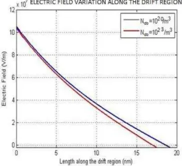
Fig.5. Electric field profile along drift length L=20nm for two different carrier concentrations (Ndb=10 20
/m3,1023/m3).
Fig. 5 represents the variation of the electric field with length along the drift region for two different
n-region doping concentration .Again as earlier the electric field is maximum at the p+-n junction as
expected where avalanche breakdown occurs and it decreases as we proceed along the drift region and
eventually it decreases to a value close to zero at the end of the depletion width which is near the N+
region. But here it is observed that the electric field decreases to zero comparatively earlier with the
increase of substrate doping concentration of the n-region as the small electric field between the n-N+
regions vanishes with the increase of doping concentration (n-region is tending to a N+ region).Thus
effectively, the extension of the depletion width in the n-region will be reduced thereby lowering the
electric field near the N+ region.
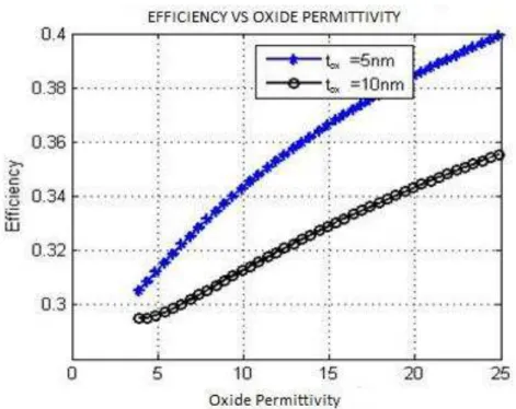
Fig. 6 represents the variation of the efficiency of this device with the oxide permittivity. The
efficiency of the device increases rapidly with the increase of oxide permittivity. With the decrease of
oxide thickness, the capacitance between the n-region and C-gate increases and so the immobile
carrier concentration decreases in the n-region. Thus, the depletion width will increase in the n-region,
thereby increasing the efficiency. By using high K dielectrics the efficiency of this device can be
increased. Moreover high K-dielectric also provides high immunity to the leakage current when the
device is in off-state.
Fig. 7 depicts the variation of the efficiency of this device with the oxide thickness. The efficiency of
the device increases with the reduction of the gate oxide thickness. Besides the efficiency of the
device increases for smaller silicon substrate thickness. Higher efficiency can be achieved for silicon
substrate thickness of 12nm compared to that of 15nm silicon substrate thickness as shown in the
the immobile carrier concentration (decreases due to changeover of the N+ region to n-region) in the
n-region and so the depletion width will increase as stated earlier and so the efficiency of the device
will also increase.
Fig. 8 represents the variation of the efficiency of this device with the oxide thickness as shown
earlier in the Fig. 7 but here the variations have been shown for two different applied voltages 0.5 V
and 0.35V.As it can be clearly observed that higher efficiency can be achieved for 0.35V compared to
the applied voltage of 0.5V .
Fig. 9 shows the variation of the efficiency of a junctionless SDR IMPATT and a normal SDR
IMPATT with the substrate carrier concentration. It can be observed that the efficiency of the
proposed device is comparatively higher for the junctionless SDR IMPATT than that of a normal
SDR IMPATT thereby making this junctionless device more attractive. It should be noted that the
maximum electric field is less in case of junctionless SDR IMPATT due to the reasons already
mentioned earlier and so the avalanche width being dependent on maximum electric field will be less
(equation 21) thereby making the efficiency of a junctionless SDR IMPATT greater than that of a
conventional SDR IMPATT.
Fig.7. Variation of efficiency of proposed junctionless SDR IMPATT device with the oxide thickness for two different silicon body thickness (tsi=12, 15 nm).
Fig.9. Variation of efficiency with the carrier concentration for a junctionless SDR IMPATT and a normal SDR IMPATT.
V. CONCLUSION
In the present work, utilizing the concept and advantages of a junctionless field effect
transistor (JLTFET), an attempt has been made to present a new device structure which will
function as a SDR (Single Drift Region) P+-N-N+ IMPATT diode .The analytical modeling
of the electric field profile and the investigation of the efficiency of the proposed device
structure have been performed based on the solution of the 2D-
Poisson’s equation. The
proposed device structure does not require any physical metallurgical junctions and no
impurity doping for creating the P+ and N+ regions. However, the voltage applied across the
P+ and N+ regions can modulate the breakdown voltage and hence the efficiency can also be
modulated. The electric field profile of our proposed structure resembles the electric field
profile of a normal SDR IMPATT diode and without any physical doping greater efficiency
can be achieved than that of a normal SDR IMPATT diode and also the efficiency can be
increased by varying oxide permittivity, oxide thickness and applied voltage. However we
feel it will be better if we decide the practical implementations only after fabrication and
detailed characterization of these devices.
REFERENCES
[2] G. Venkateshwar Reddy and M. Jagadesh Kumar ,”A New Dual-Material Double-Gate (DMDG) Nanoscale SOI MOSFET—Two-Dimensional Analytical Modeling and Simulation,“ IEEE Trans. NanoTechnology, S, vol. 4, no. 2, pp. 260-268,March 2005.
[3] Bibhas Manna, Saheli Sarkhel, Nurul Islam, S. Sarkar, and Subir Kumar Sarkar,”Spatial Composition Grading of Binary Metal AlloyGate Electrode for Short-Channel SOI/SON MOSFET Application”, IEEE Trans. Electron Devices, S, vol. 59, no.12, pp.3280-3287,December 2012.
[4] Sourav Naskar and Subir Kumar Sarkar,”Quantum Analytical Model for Inversion Charge and Threshold Voltage of Short-Channel Dual-Material Double-Gate SON MOSFET,”IEEE Trans. Electron Devices, S, vol. 60, no. 9, pp. 2734-2740,September 2013.
[5] Sharmistha Shee, Gargee Bhattacharyya, and Subir Kumar Sarkar,”Quantum Analytical Modeling for Device Parameters and I –V Characteristics of Nanoscale Dual-Material Double-GateSilicon-on-Nothing MOSFET,” IEEE Trans. Electron Devices, S, vol. 61, no. 8, pp. 2697-2704,August 2014.
[6] Xiaoshi Jin, Xi Liu, Hyuck-In Kwon, Jung-Hee Lee, Jong-Ho Lee,”A subthreshold current model for nanoscale short channel junctionless MOSFETs,” Solid-State Electronics vol. 82 ,pp. 77–81,Oct 2013.
[7] Lee CW, Afzalian A, Akhavan ND, Yan R, Ferain I, Colinge JP.,”Junction-less multigate field-effect transistor”, J. Appl. Phys., vol. 94(5), pp. 053511-053511-2, Feb.2009.
[8] Lee CW, Borne A, Ferain I, Afzalian A, Yan R, Akhavan ND, “Hightemperature performance of silicon junctionless MOSFETs”, IEEE Trans. Electron Devices, S, vol. 57, no. 3, pp. 620-5,March 2010.
[9] Park CH, Ko MD, Kim KH, Baek RH, Sohn CW, Baek CK, “Electricalcharacteristics of 20-nm junctionless Si nanowire transistors,”Solid-State Electron,vol. 73, pp.7–10, July 2012.
[10]Ansari L, Feldman B, Fagas G, Colinge JP, Greer JC. ,”Subthreshold behavior of junctionless silicon nanowire transistors from atomic scale simulations,” Solid-State Electron.,vol. 71,no. 11,pp. 58–62,May 2012.
[11]Colinge JP, Lee CW, Afzalian A, Akhavan ND, Yan R, Ferain I, “Nanowire transistors without junctions,” Nature Nanotech.,vol. 5,pp. 225–9, Feb 2010.
[12] Dalle C, Rolland P, Lieti G ,”Flat doping profile double-drift silicon IMPATT for reliable CW high power high-efficiency generation in the 94-GHz window,” IEEE Trans. Electron Devices, S, vol. 37, no. 1, pp. 227-236, Jan 1990.
[13]Luy JF, Casel A, Behr W, Kasper E,”A 90-GHz double-drift IMPATT diode made with Si MBE,”IEEE Trans. Electron Devices, S, vol. 34, no. 5, pp. 1084-1089, May 1987.
[14]Luschas M, Judaschke R, Luy JF (2002b),”Simulation and measurement results of 150 GHz integrated silicon IMPATT diodes”, in IEEE MTT-S International Microwave Symposium Digest June 2002, vol.2,pp 1269–1272.
[15]Tapas Kumar Pal1 and J. P. Banerjee2, “Study of Efficiency of Ka-band IMPATT Diodes and Oscillators around Optimized condition,” International Journalof Advanced Science and Technology ,vol. 26, Jan 2011 .
[16]D. Ghosh, B. Chakrabarti, M. Mitra “A Detailed Computer Analysis of SiC And GaN Based IMPATT Diodes Operating at Ka, V And WBand”, International Journal of Scientific & Engineering Research, vol. 3(2), Feb 2012 1,ISSN 2229-5518.
[17] L. P. Mishra , S. Chakraborty , M. Mitra, “A Computer Method for studying unction Depth of SDR IMPATTdiode and a Comparisonofits Performance Based different SemiconductorMaterials”, International Journal of Engineering Science and Technology (IJEST), vol. 3,no. 6 ,June 2011, ISSN : 0975-5462.
[18]Yogesh Goswami,Bahnimann Ghosh and Pranav Kumar Asthana, “Analog performance of Si junctionless tunnel field effect transistor and its improvisation using III-v semiconductor,” RSC Adv.,vol. 4, pp. 10761–10765,Jan 2014, DOI: 10.1039/c3ra46535g.
[19]M.W.Akram,Bahniman Ghosh,Punyasloka Bal,Partha Mondalm, ”P-type double gate junctionless tunnel field effect transistorm,” Journal of Semiconductors,vol.35,no.1, Jan 2014.
[21]K.Konrad Young,” Short-Channel Effect in Fully Depleted SO1MOSFET's,” IEEE Trans. Electron Devices,vol. 36, no. 2, pp.399-402,Feb 1989.
[22]F. Jazaeri, L. Barbut, A. Koukab, J.-M. Sallese, “Analytical model for ultra-thin body junctionless symmetric double gate MOSFETs in subthreshold regime, ”Solid-State Electronics ,vol. 82 , pp. 103–110, Apr.2013.
[23]MS.Tyagi,”Introduction to Semiconductor materials and Devices,” John Wiley & Sons, Inc., Hoboken, New Jersey 1991 ,pp. 312-317.