Abstract - A structure shaped substrate wideband microstrip patch antenna fed by coplanar waveguide (CPW) is proposed for wireless applications. Structure shaped substrate is produced by cutting the rectangle shape substrate in the form of a semicircular disc. The radiating patch of proposed antenna is taken in the form of U-shape. The ground plane is extended towards both sides of radiator for reducing the size of the antenna. The proposed antenna is simulated by Ansoft’s High Frequency Structure Simulator (HFSS). A good agreement is observed between simulated and measured results. The prototype is taken with dimensions 24 mm × 24 mm ×1.6 mm that achieves wide bandwidth, constant group delay and good radiation patterns over the entire operating bandwidth from 3.4 to 9.4 GHz (6.0 GHz) with 93.7% impedance bandwidth at 6.4 GHz center frequency. Thus, the proposed antenna is applicable for C band applications.
Index Terms— CPW-Fed, Microstrip Antenna, Structured Substrate, Wideband.
I. INTRODUCTION
With the fast development in wireless communication, the demand for devices that can operate for
wideband has increased [1-4]. A lot of research work has carried out on wideband and ultrawideband.
Many different types of patch antenna shapes such as circular shape [5], U shape [6], inverted T shape
[7], M shape [8], A shape [9], rhombus shape [10] etc. are used till now for getting wideband. Along
with these different types of shapes researchers also work on numerous techniques and structures for
getting wideband such as CPW-fed technique and defected ground structure for getting wideband
[11-16]. Substrate of microstrip patch antennas also plays a major role for obtaining wideband [17]. In
these types of microstrip patch antennas a common thing is that the substrate is taken either
rectangular or square in shape. In these shapes the large space around the radiator is generally wasted.
A CPW-Fed Structure Shaped Substrate
Wideband Microstrip Antenna for Wireless
Applications
1Amar Sharma, 2Puneet Khanna, 3Arun Kumar
1,2,3Department of Electronics and Communication Engineering, SET, IFTM University, Moradabad-244102, India. Email: [email protected], [email protected], [email protected]
4
Kshitij Shinghal
Journal of Microwaves, Optoelectronics and Electromagnetic Applications, Vol. 16, No. 2, June 2017
DOI: http://dx.doi.org/10.1590/2179-10742017v16i2805
420
achieve wide bandwidth. The advantage of structure shaped substrate is that it helps to reduce the
overall size of the antenna with wide impedance bandwidth. The large space around the radiator is
fully utilized by placing the ground and radiating patch on single side of the substrate. The proposed
antenna is composed of U-shape radiating patch with good radiation performance from 3.4 to 9.4
GHz. The detailed antenna geometry is discussed in section 2. Section 3 covers the parametric study
of proposed antenna in detail. Experimental results are discussed in section 4. Section 5 concludes the
paper.
II. ANTENNA GEOMETRY
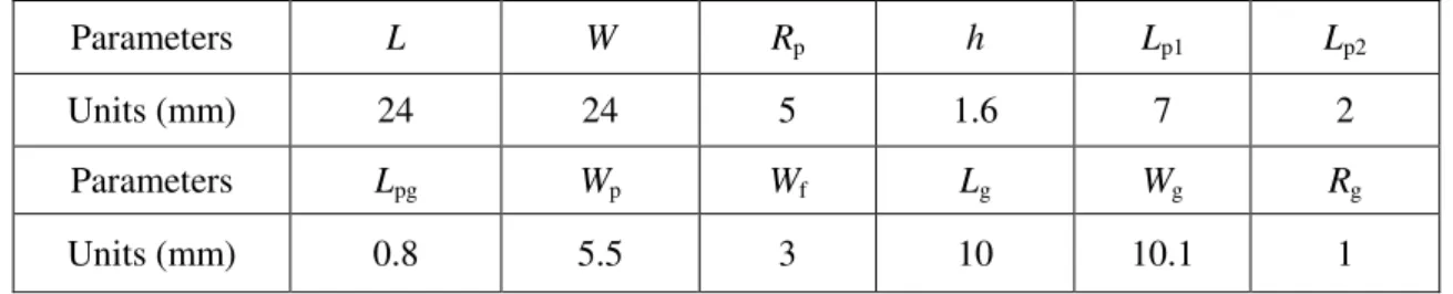
The schematic configuration of the proposed CPW-fed structure-shape substrate wideband antenna
is shown in Fig. 1. The proposed antenna has overall dimensions of L×W and is designed and
fabricated on a low-cost FR4 substrate of thickness h, relative permittivity εr = 4.4 and loss tangent
tanδ = 0.0019. The substrate is etched in the form of semicircular disc at the centre with radius 12
mm. The radiating patch is in the shape of rectangle and a circular disc of radius (Rp) is etched in the
middle of patch. The center position of circular disc is at the distance of Lp2 from upper side of the
radiator. The ground plane is on the same plane as radiator. It has two rectangular slits each having
dimensions Wg × Lg and a semicircular path having thickness (Rg) . The length of gap between the
radiating patch and the ground plane is taken as Lpg. The width of CPW- fed line is fixed at Wf to
achieve 50 ohm characteristics impedance. Since the radiator is surrounded by a metal ground plane
on the etched substrate it helps in reducing the size of proposed antenna. The small area between the
radiator and the ground is a major factor for achieving strong capacitive coupling. The gap between
the feed and ground plane is taken as 0.4mm. The detailed dimensions of the proposed defected
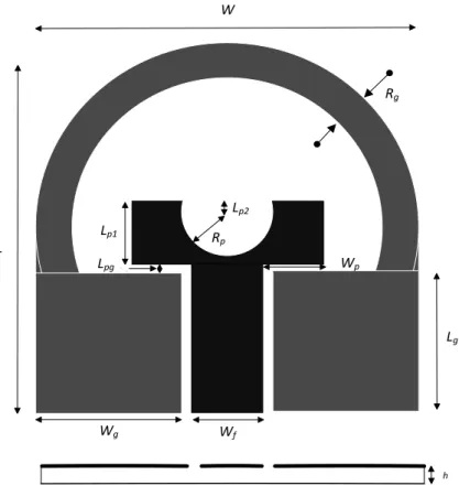
substrate CPW- fed wideband antenna are listed in Table 1. Fig. 2 illustrates the photograph of
fabricated antenna, which is connected with a 50Ω SMA connector for measurement of the
parameters.
Table 1. Design parameters of the proposed CPW-fed structure-shape substrate wideband antenna
.
Parameters L W Rp h Lp1 Lp2
Units (mm) 24 24 5 1.6 7 2
Parameters Lpg Wp Wf Lg Wg Rg
Units (mm) 0.8 5.5 3 10 10.1 1
The electromagnetic solver, Ansoft HFSS (v 14.0) [19], is used to investigate and optimize the
proposed antenna configuration. The various modifications of the ground plane and substrate are
shown in Fig. 3. Firstly, two rectangular slots on rectangular substrate (trace (i)) is used, the
resonating bands at 4.25 and 9.0 GHz and does not cover the entire operating bandwidth. However,
when ground plane on rectangular substrate is stretched to form a circular ring shape ground (trace
(ii)), the simulated return loss shows better results but not covers the entire bandwidth as return loss is
above 10dB only from frequencies 5.8 to 7.6 GHz, with two resonating bands at 4.6 and 8.67 GHz.
Furthermore, when substrate is etched in the form of semicircular disc (trace (iii)), the simulated
return loss shows good results covering the entire bandwidth with two resonating bands at 4.4 and 8.0
GHz , having larger impedance bandwidth compared to trace (i) and (ii). Finally, it is decided to take
etched substrate antenna for the proposed design because it is smaller than rest of the design with
better impedance matching conditions for the entire bandwidth from 3.4 to 9.4 GHz (6.0 GHz).
Wg L
W
Wf
Rp
Lp1
Wp
Lpg
Rg
h Lp2
Lg
Journal of Microwaves, Optoelectronics and Electromagnetic Applications, Vol. 16, No. 2, June 2017
DOI: http://dx.doi.org/10.1590/2179-10742017v16i2805
422
Fig. 2. Photograph of the proposed CPW-fed structure-shape substrate wideband antenna.
Fig. 3. Simulated return loss against frequency for the proposed CPW-fed structure-shape substrate wideband antenna, ring shape ground plane and two rectangular slots antenna.
III. PARAMETRIC STUDY OF THE PROPOSED ANTENNA
In this section, the influence of the different design parameters on antenna performance is studied
and discussed. At a time one parameter is taken, the others are kept constant. The result of these
parametric studies provides a useful strategy to optimize the design before final fabrication. The effect Radiator
Two rectangular slots
(i) (ii) Ring Shape Proposed
Antenna (iii) (i)
(ii)
of change in radiating patch length, width, inner circle radius (Lp1,Wp , Rp), microstrip feed line (Wf),
ground plane semicircular path (Rg) and length between radiating patch and ground plane (Lpg) are
considered for parametric study.
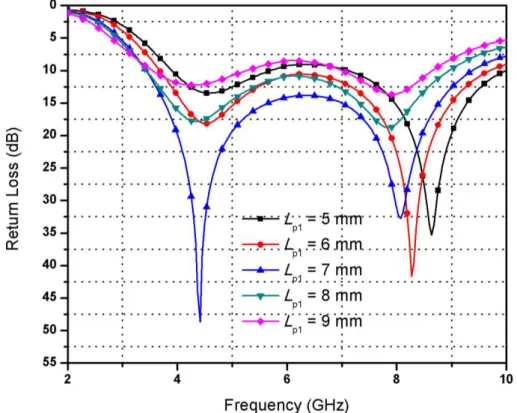
Fig. 4 depicts the effect of the length Lp1 of the radiating patch from 5 to 9 mm. It is found that the
bandwidth of antenna increases when the value of Lp1 increases from 5 to 7 mm. With further increase
in length, it deteriorates. Therefore, it is decided to take Lp1 = 7 mm as the optimum value for the
bandwidth from 3.4 to 9.4 GHz, covering the entire wideband.
The effect of the width Wp of radiating patch on the impedance bandwidth of the antenna from 5.0
to 6.0 mm is depicted in Fig. 5. It can be seen from the graph that the bandwidth of the antenna
increases as the value of Wp increases from 5.0 to 5.5 mm. With further increase in width, it
deteriorates. Therefore, it is decided to take Wp= 5.5 mm as the optimum value covering the entire
wideband.
Journal of Microwaves, Optoelectronics and Electromagnetic Applications, Vol. 16, No. 2, June 2017
DOI: http://dx.doi.org/10.1590/2179-10742017v16i2805
424
Fig. 5.Simulated return loss against frequency for the proposed CPW-fed structure-shape substrate wideband antenna with various Wp ; other parameters are the same as listed in Table 1.
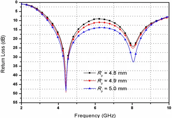
Fig. 6 shows the effect on the radius of inner circle of U -shape radiating patch (Rp) on the return
loss of the proposed antenna. It is keenly observed that by changing the value of Rp from 4.8 to 5.0
mm, the bandwidth of return loss increases with increase in Rp. Therefore, it is decided to take Rp =
5.0 mm as the optimum value, covering the entire wideband.
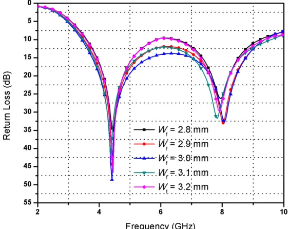
Fig. 7 illustrates the effect of the microstrip feed line width Wf on the return loss of the proposed
antenna from 2.8 to 3.2. It is observed that by changing the value of Wf from 2.8 to 3.0 mm, the
impedance matching improves at 5 to 7 GHz. With further enhancement in microstrip feed line width
(Wf), it deteriorates. Therefore, it is decided to take Wf = 3.0 mm as the optimum value.
Fig. 7.Simulated return loss against frequency for the proposed CPW-fed structure-shape substrate wideband antenna with various Wf ; other parameters are the same as listed in Table 1.
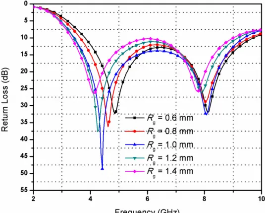
It is worth mentioning that the configuration of the ground plane also affects the characteristics of
patch antenna. Thus, the semicircular path (Rg) of the structure shape substrate is also considered for
the parametric study. Fig. 8 shows the simulated return loss as Rg varies from 0.6 to 1.4 mm in step of
0.2 mm. It can be seen that the bandwidth of return loss increases as Rg varies from 0.6 to 1.0 mm and
decreases with further increase in Rg. It is also observed that impedance mismatch of the total band
also improved as Rg varies from 0.6 to 1.0 mm and decreases further. Therefore, it is decided to take Rg= 1.0 mm as the optimum value with the bandwidth from 3.4 to 9.4 GHz, covering the entire wide
Journal of Microwaves, Optoelectronics and Electromagnetic Applications, Vol. 16, No. 2, June 2017
DOI: http://dx.doi.org/10.1590/2179-10742017v16i2805
426
Fig. 8.Simulated return loss against frequency for the proposed CPW-fed structure-shape substrate wideband antenna with various Rg ; other parameters are the same as listed in Table 1.
Fig. 9 shows the effect of length between patch and ground Lpg from 0.6 to 1.4 mm on antenna
performance. The bandwidth of return loss increases as the value of Lpg increases from 0.6 to 0.8 mm.
As the value of Lpg increases further, the bandwidth of return loss degrades. Thus, the optimum value
of the length between patch and ground (Lpg) of the proposed antenna is chosen to be 0.8mm.
The results obtained from the variation of different parameters, it is clear that due to structure shape
substrate, the proposed antenna has wide impedance bandwidth performance without increasing the
Fig. 9.Simulated return loss against frequency for the proposed CPW-fed structure-shape substrate wideband antenna with various Lpg ; other parameters are the same as listed in Table 1.
IV. EXPERIMENTAL RESULT AND DISCUSSION
The performance of the proposed antenna such as return loss, group delay and radiation pattern are
measured using Agilent 8757E scalar analyzer. For manufacturing the proposed antenna, dielectric
substrate FR4 (Fire Retardant) having relative permittivity εr = 4.4 is used. The value of loss tangent for this dielectric material is tanδ= 0.0019. FR4 is a composite material composed of woven fiber glass cloth with an epoxy resin binder that is flame resistant. The proposed antenna was printed
through milling technique done with the help of MITS, Eleven Lab machine. In milling process the
removal of extra copper on FR4 sheet is done through machine without using any chemical. Milling
process is typically a non-chemical process and it can be completed in a lab environment without
exposure to hazardous chemicals.
The measured and simulated return loss curves of the proposed are shown in Fig. 10. A good
agreement is observed between simulated and measured results. The small difference between
measured and simulated result is due to the effect of SMA (sub miniature version A) connector
soldering and fabrication tolerance. This small difference is also due to the impingement of the
Journal of Microwaves, Optoelectronics and Electromagnetic Applications, Vol. 16, No. 2, June 2017
DOI: http://dx.doi.org/10.1590/2179-10742017v16i2805
428
(1)
where is the phase constant. The , and are the permittivity, permeability in the
SMA connector, and the angular frequency, respectively.
SMA connectors are commonly used for microwave measurements. Connectors are necessary to
connect cables in such systems. The modeling of SMA connectors is either neglected in the
simulation of microwave components or approximated by an inaccurate model to model its
characteristics [20]. The outer structure and receptacle of the SMA connector are modeled because the
electromagnetic field affects them. A lumped port with 50Ω characteristic impedance is used for
excitation in the simulation. The designed antenna offers a bandwidth of 6.0 GHz (3.4 to 9.4 GHz)
which meets the bandwidth requirements for C band applications.
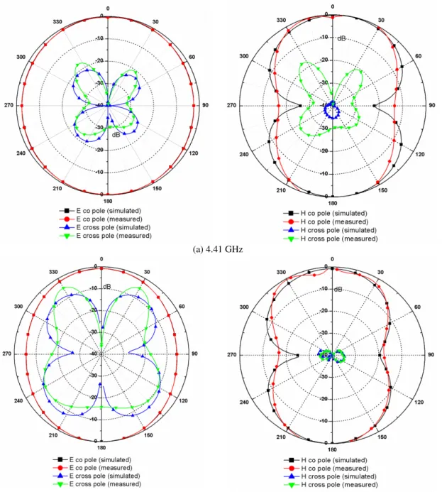
The proposed antenna illustrates good radiation pattern characteristics as shown in Fig. 11(a) to
11(b). The radiation patterns in H and E planes are at sampling frequencies of 4.4 and 8.0 GHz
respectively. Patterns are distorted because the ground plane is a part of loop path, the surface current
on the radiating plane changes the effective current distribution of the loop and results in distortion.
These patterns are suited for application in almost all wireless communication equipment, as
expected. Measured and simulated of radiation patterns shows good agreement.
(a) 4.41 GHz
(b) 8.0 GHz
Fig. 11. Radiation patterns at various frequencies of proposed CPW-fed structure-shape substrate wideband antenna (a) 4.4 GHz and (b) 8.0 GHz
The antenna gain variation with frequency is shown in Fig. 12 for the proposed antenna. Antenna
gain varies from 0.8 to 2.1 dBi over the entire operating band. Simulated result of gain shows good
Journal of Microwaves, Optoelectronics and Electromagnetic Applications, Vol. 16, No. 2, June 2017
DOI: http://dx.doi.org/10.1590/2179-10742017v16i2805
430
Fig. 12. Simulated and measured gain against frequency for the proposed CPW-fed structure-shape substrate wideband antenna.
Fig. 13 illustrates the group delay of the proposed antenna. Group delay is an important parameter
in the designing of wideband antenna as it shows about the distortion of the transmitted pulses in all
wireless communications. The group delay is obtained from the derivative of the phase variation with
respect to angular frequency [21]. The group delay of the proposed antenna is simulated and
calculated through electromagnetic solver, Ansoft HFSS (v 14.0). It is observed that the group delay
for the proposed antenna is constant and less than 1 ns for entire operating bandwidth from 3.4 to 9.4
Fig. 13. Group delay for the proposed CPW-fed structure-shape substrate wideband antenna.
Table 2 shows the comparison of proposed (structure-shaped substrate) antenna with some other
existing antennas in terms of the antenna purpose, antenna size, operating frequency band, Impedance
bandwidth and applications. The comparative chart shows that the proposed antenna has small size,
structure-shaped substrate and wideband applications with respect to other antenna of different
dimension and shapes.
Table 2: Comparison of Reference antennas in term of size and bandwidth
Reference No.
Antenna purpose
Antenna Size (mm2)
Operating frequency band
(GHz)
Impedance Bandwidth
(%)
Applications
[5] UWB 39×40 2.6 - 12.3 129.35 UWB [10] UWB 19×21 2.78 – 12.92 129 UWB [11] Wideband 38×25 2.4 – 6.0 85.71 WLAN/WiMAX [12] Dual Band 35.24×26.4 3.424 – 6.274 19.44 & 33.19 WLAN/WiMAX [18] UWB 18×25 4.5-13.5 100 C and X band Proposed
Antenna
Wideband 24×24 3.4 -9.4 93.7 C band
Journal of Microwaves, Optoelectronics and Electromagnetic Applications, Vol. 16, No. 2, June 2017
DOI: http://dx.doi.org/10.1590/2179-10742017v16i2805
432
loss, antenna gain and radiation patterns. The radiation patterns are satisfactory over the entire
operating bandwidth. Also, almost constant group delay is achieved. The proposed antenna gives
impedance bandwidth of about 93.7% which helps its use in various wireless applications.
REFERENCES
[1] M.K. Khandelwal, B.K. Kanaujia, S. Dwari, S. Kumar, and A.K. Gautam. “Analysis and design of wideband microstrip-line-fed antenna with defected ground structure for Ku band applications,” AEU-International Journal of Electronics and Communication, 2014. vol.68, No.10, pp 951-957.
[2] L. Sun, M. He, J. Hu, Y. Zhu, and H. Chen. “A butterfly-shaped wideband microstrip patch antenna for wireless communication,” International Journal of Antenna and Propagation, Hindawi, 2015. vol. pp 1-8.
[3] H.F. Abutarboush, R. Nilavalan, S.W Cheung, K.M. Nasr, T. Peter, D. Budhimir, and H.A. Raweshidy. “A reconfigurable wideband and multiband antenna using dual-patch elements for compact wireless device,” IEEE Transactions on Antennas and Propagation, 2012. vol. 60, pp 36-43.
[4] X. L. Bao, M.J. Ammann, and P. McEvoy. “Microstrip-fed wideband circularly polarized printed antenna,” IEEE Transactions on Antennas and Propagation, 2010. vol. 60, pp 3150-3156.
[5] R. Azim, M.T. Islam, and N. Misran. “Microstrip line fed printed planar monopole antenna for UWB applications,” Springer Arab Journal Science and Engineering, 2013. vol.38, pp 2415-2422.
[6] N.K. Darimireddy, R. Ramana Reddy, and A. Malikarjuna Prasad. “Design of triple-layer double U-slot patch antenna for wireless communication,” Journal of Applied Research and Technology, 2015. vol.13, No.5, pp 526-534.
[7] P. Khanna, A. Sharma, K. Shinghal, and A. Kumar. “A defected structure shaped CPW- fed wideband microstrip antenna for wireless communication,” Journal of Engineering Hindawi,2016. vol. 2016, pp 1-7.
[8] M.K. Shrivastava, A.K. Gautam, and B.K. Kanaujia. “An M-shaped monopole-like slot UWB antenna,” Microwave and Optical Technology Letters, 2014. vol.56, pp 127-131.
[9] M.K. Shrivastava, A.K. Gautam, and B.K. Kanaujia. “A novell A-shaped monopole-like slot antenna for ultra wideband applications,” Microwave and Optical Technology Letters, 2014. vol.56, pp 1826-1829.
[10] R. Chandel, A.K. Gautam, and B.K. Kanaujia. “A compact rhombus-shaped slot antenna fed by microstrip-line for UWB applications,” International Journal of Microwave and Wireless Technologies, 2015. pp 1-7.
[11] A.K. Gautam, A. Bisht, and B.K. Kanaujia. “A wideband antenna with defected ground plane for WLAN/ WiMAX applications,” AEU-International Journal of Electronics and Communication, 2016. vol. 70, No.3, pp 354-358.
[12] D. Prakash and R. Khanna. “Design and development of CPW-fed microstrip antenna for WLAN/WiMAX applications”, Progress in Electromagnetic Research C, 2010. vol.12, pp 17-27.
[13] J. Pourahmadazar, Ch. Ghobadi, J. Nourinia, N.Felegari, and H. Shirzad. “Broadband CPW-fed Circularly polarized square slot antenna with inverted-L strips for UWB applications,” IEEE Transactions on Antennas and Propagation Letters, 2011. vol. 10, pp 369-372.
[14] J.Y Sze, C.G. Hsu, and J. Shiu. “Small CPW-fed band-notched ultra wideband rectangular aperture antenna,” IEEE Transactions on Antennas and Propagation Letters, 2008. vol. 7, pp 513-516.
[15] G. K. Pandey, H. S. Singh, P. K. Bharti, and M. K. Meshram. “Design and Analysis of -shaped UWB Antenna with Dual Band Notched Characteristics,” Wireless Personal Communication, 2016. vol. 89, pp 79-92.
[16] S. Kumar, B. Kr. Kanaujia, S. Dwari, G. P. Pandey, and D. K. Singh. “Analysis and design of switchable rectangular monopole antenna using asymmetric cross slot for wireless communication,” Wireless Personal Communication, 2016. vol. 89, pp 79-92.
[18] Karlo Q. da Costa and Victor Dmitriev. “Planar Monopole UWB Antenna with Cuts at the Edges and Two Parasitic Loops,” Journal of Microwaves, Optoelectronics and Electromagnetic Applications, 2009. vol. 8, No. 1, pp 92-100.
[19] Ansoft Corporation, Ansoft High-Frequency Structure Simulator (HFSS) version 14.0, Ansoft Corporation, Pittsburgh, PA.
[20] T. Hirano, J. Hirokawa, and M. Ando. “Influence of the SMA Connector and its Modeling on Electromagnetic Simulation,” Microwave and Optical Technology Letters, 2015. vol. 57, No. 9, pp. 2168-2171.