João Francisco Carvalho Paulo
Licenciado em Ciências de Engenharia de Micro e Nanotecnologias
Resistive switching RAM devices based
on amorphous oxide semiconductors for
system on panel applications
Dissertação para obtenção do Grau de Mestre em
Engenharia de Micro e Nanotecnologias
Orientador: Jonas Deuremeier, Doctoral Researcher, NOVA University of Lisbon
Co-orientadora: Asal Kiazadeh, Doctoral Researcher, NOVA University of Lisbon
Júri
Presidente: Doutor Rodrigo Ferrão de Paiva Martins Arguente: Doutor Pedro Miguel Cândido Barquinha
Resistive switching RAM devices based on amorphous oxide semiconductors for system on panel applications
Copyright © João Francisco Carvalho Paulo, Faculdade de Ciências e Tecnologia, Univer-sidade NOVA de Lisboa.
A Faculdade de Ciências e Tecnologia e a Universidade NOVA de Lisboa têm o direito, perpétuo e sem limites geográficos, de arquivar e publicar esta dissertação através de exemplares impressos reproduzidos em papel ou de forma digital, ou por qualquer outro meio conhecido ou que venha a ser inventado, e de a divulgar através de repositórios científicos e de admitir a sua cópia e distribuição com objetivos educacionais ou de inves-tigação, não comerciais, desde que seja dado crédito ao autor e editor.
Este documento foi gerado utilizando o processador (pdf)LATEX, com base no template “novathesis” [1] desenvolvido no Dep. Informática da FCT-NOVA [2].
Acknowledgements
Firstly, would like to thank faculty of FCT-UNL for their support and guidance during my journy, specially all the teachers and investigators from DCM, CENIMAT.
I would like to thank my supervisors Jonas Deuermeier and Asal Kiazadeh along with the project NeurOxide (PTDC/NAN-MAT/30812/2017).
Quero também agradecer à Maria Pereira, Jorge Martins, Emanuel Carlos e Ângelo Santos pelo apoio na fabricação, na caracterização e no design da máscara.
Quero ainda agradecer aos meus colegas e amigos pelo apoio nos últimos 5 anos. Finalmente quero agradecer aos meus pais, ao meu irmão e aos meus avós, em especial ao meu avô João.
Abstract
This work reports the mask design, fabrication and characterization of memristor devices with diode like electrical behavior at pristine state. It is due to the presence of Schottky junctions between Zinc-tin-oxide (ZTO) and platinum - Indium-gallium-zinc-oxide (IGZO) and molybdenum oxide for two different Metal-Insulator-Metal (MIM) configurations. The devices were exclusively produced using physical vapor deposition processes without intentional heating. Typical advanced electrical analysis of ReRAM device was performed.
The Pt-ZTO-TiAu devices showed pinched hysteresis properties with large Ron/of f
ratio, fast switching which can be controlled in a digital SET and analog RESET operation. However, large device-to-device variations and stability are the main issues which is due to the processing.
On the other hand, the Mo-IGZO-Mo devices showed a small Ron/of f ratio and only
analog operation. There was a high yield and stability. However, using DC sweep for cycling led to a charging phenomenon. Using SET/RESET pulses, the devices sustain hundreds of cycles without deterioration or movement of the resistance states, showing great resilience and retention.
Keywords: ReRAM, memristor, ZTO, IGZO, resistive switching memory, transparent electronic.
Resumo
Este trabalho relata a projecção de mascaras, fabricação e caracterização de memris-tores com comportamento elétrico de diodo em estado intocado. É devido à presença de junções Schottky entre ZTO e platina - IGZO e óxido de molibdênio para duas confi-gurações diferentes de MIM. Os dispositivos foram produzidos exclusivamente usando processos físicos de deposição de vapor em temperatura ambiente. A análise elétrica avançada típica dos dispositivos ReRAM foi realizada.
Os dispositivos Pt-ZTO-TiAu mostraram propriedades de histerese comprimida com uma grande proporção Ron/of f, comutação rápida que pode ser controlada em operação
digital SET e analógica RESET. No entanto, grandes variações de dispositivo a dispositivo e estabilidade são os principais problemas causados pelo processamento.
Por outro lado, os dispositivos Mo/IGZO/Mo mostraram uma pequena proporção
Ron/of f e apenas operação analógica. Houve um alto rendimento e estabilidade. No
en-tanto, o uso do varrimento DC para a realização de ciclos levou a um fenômeno de car-regamento. Usando pulsos SET/RESET, os dispositivos suportam centenas de ciclos sem deterioração ou movimento dos estados de resistência, mostrando grande resiliência e retenção.
Palavras-chave: RRAM, memristor, ZTO, IGZO, memória de comutação resistiva, eletrô-nica transparente.
Contents
List of Figures xiii
Glossary xv
Acronyms xvii
1 Motivation 1
2 State of the art 3
2.1 Thin-film devices . . . 3
2.2 Memristors . . . 3
2.2.1 Memristor mechanisms . . . 4
2.2.2 HP Lab’s 2008 memristor . . . 6
2.3 Digital and analog memristors . . . 6
2.4 Digital memories . . . 7
2.5 Problems and solutions . . . 8
3 Materials and Methods 11 3.1 Mask for photolithography . . . 11
3.2 Device fabrication . . . 13
3.2.1 Thin film depositions . . . 13
3.2.2 Patterning . . . 14
3.3 Device characterization . . . 14
3.3.1 XPS analysis . . . 14
3.3.2 Electrical DC characterization . . . 14
3.3.3 Electrical pulse characterization . . . 15
4 Results 17 4.1 Non-patterned Pt-ZTO-TiAu memristors . . . 17
4.2 Patterned Pt-ZTO-TiAu memristors . . . 18
4.2.1 Set and reset . . . 18
4.2.2 Gradual reset and digital set . . . 18
4.2.3 Pulse speed testing and operation . . . 19
C O N T E N T S
4.3 Patterned Mo-IGZO-Mo memristors . . . 22
4.3.1 Pristine state, set and reset . . . 22
4.3.2 Cycling and retention . . . 25
4.3.3 Pulsed speed and operation . . . 26
5 Conclusions and future prospects 29 5.1 Conclusions . . . 29 5.2 Future prospects . . . 29 Bibliography 31 I Annex 35 I.1 Annex A . . . 35 I.2 Annex B . . . 36 xii
List of Figures
2.1 The first graph is a typical I-V curve of a memristor, the second graph shows the memristor’s resistance changing with successive voltage sweeps. [6] . . . 4 2.2 Several possible mechanisms for reversible resistive switching. . . 5 2.3 a,b and c are filamentary devices. a) illustrates the electroforming step. b)
illustrates a valence change device working (bipolar). c) illustrated a thermo-chemical device working (unipolar). d) Illustrates a an area dependent bipolar device based on oxygen ion migration. [12] . . . 5 2.4 a) is an illustration of a single memristor in crossbar configuration and b) is a
AFM image of a crossbar array.[13] . . . 6 2.5 a) a memristor array without selector. b) a memristor array with a selector this
can require extra wires here is depicted the worst case scenario with 2 extra wires. [24] . . . 8 3.1 a) cross-section of the Mo-IGZO-Mo devices, b) cross-section of the
Pt-ZTO-TiAu devices. . . 11 3.2 Mask design . . . 12 4.1 a) Typical pristine state, showing some rectification b) Digital set and analog
reset for non-patterned device. . . 17 4.2 a) Digital set and reset for a patterned 5 µm squared device , CC of 5/8 × 10−5
A was used and b) retention at 0.1 V for ∼1000 s . . . 18 4.3 Digital set with a CC of 1×10⁻⁵ A . . . 19 4.4 a) Initialization from a device with high current pristine state, b) mulriple
gradual reset with 5, 3 and 5 different states , c) and d) gradual reset with MLC approach. . . 20 4.5 Digital set and reset of the device used in the pulse speed testing, note that for
speed testing set was initially done in transient. . . 20 4.6 Reset speed test, pulses are divided into 2 plots each, a top one with readout
current at 0.1 V and a bottom one with the input 1 V pulse, from left to right there is 100us, 50us, 100ns, 10ns, 75ns and 90ns, 100ns, 95ns, 99ns and 100ns. 21 4.7 Set and reset done entirely with pulses, pulses are divided into 2 plots the top
L i s t o f F i g u r e s
4.8 The first graph is the pristine state of several devices, the second graph shows the electroforming process using current sweep for some devices of different sizes. [6] . . . 22 4.9 Pristine state for the IGZO devices, with pronounced rectification. . . 23 4.10 Initialization and analog set and reset. . . 23 4.11 XPS depth profile. We can observe the change in ratio along the depth, this is
typical of homogeneous oxygen migration mechanisms. [12] . . . 24 4.12 Reset for devices with square sizes of 2 um and 20 um. The arrows indicate
the curve zone used for measuring the current. . . 24 4.13 a) Current variation with device area and b) Current density variation with
size, as can be seen there is a clear linear relation between current and area. . 25 4.14 Set and reset cycling and retention states. . . 25 4.15 Cdf of 100 cycles after set and reset . . . 26 4.16 Testing pulse speed with Mo-IGZO-Mo device, reading at 0.1 V with Keithley
in blue and pulse generated by Keysight wave generator in orange, arrows indicate a pulse. From top to bottom : set 1 s, 100 ms and 10 ms width pulses at -1 V, reset 1 s, 100 ms and 10 ms width pulses at 1.5 V. . . 27 4.17 Cdf of 300 cycles (first 150 and last 150 cycles). . . 28 4.18 Comparison between the first 150 cycles (darker) and the last 150 cycles
(ligther). . . 28 I.1 Shadow mask for deposition of top electrodes, the sizes are, from top to bottom
500 µm, 600 µm, 700 µm, 800 µm, 900 µm, 1000 µm. . . 35 I.2 Current density variation with area of Pt-ZTO-TiAu memristors, as we can
see the current density is not constant and there is no obvious relation. The higher currents for very large areas could be due to the increased probability of impurities. The instability of the devices prevented us from testing current densities in HRS and LRS and infer filamentary or area dependent behavior. 36
Glossary
Analog memristor A memristor that can have any resistance between HRS and LRS and gradual set and reset.
Bipolar A memristor whose set and reset require voltages with opposite polarities.
Digital memristor A memristor with an abrupt set and reset, generally has a large operating window.
High resistance state The state of the device with the highest possible resistance while in operation i.e.: still possible to revert to an LRS and back to HRS. It is equivalent to Low conductance state (LCS).
Low resistance state The state of the device with the lowest possible resistance while in operation i.e.: still possible to revert to an HRS and back to LRS. It is equivalent to High conductance state (HCS).
Pristine state The state of the devices immediately after fabrication, measuring the pristine state is done by measuring an I-V curve with voltages small enough so the resistance of the device is not altered.
Reset A process by which the memristor’s resistance increases. Set A process by which the memristor’s resistance decreases. Switching time The pulse width of a single pulse required to change the
G L O S S A RY
Threshold voltage A voltage after which set or reset happens, in digital mem-ristors this voltage is the set/reset voltage, in gradual memristors after this voltage the memristor resistance changes but before the device can be read without dis-turbing its resistance.
Unipolar A memristor whose set and reset use voltages with the same polarity but with differing magnitudes.
Acronyms
1D1M 1-Diode-1-Memristor. 1T1C 1-Transistor-1-Capacitor. 1T1M 1-Transistor-1-Memristor.
AOS amorphous oxide semiconductor. BE Bottom electrode.
CC current compliance.
Cdf cumulative distribution function. DRAM Dynamic Random access memory. FeRAM Ferroelectric RAM.
FG floating gate.
HRS High resistance state. IGZO Indium-gallium-zinc-oxide. ITO Indium-Tin oxide.
LCD Liquid crystal display. LRS Low resistance state.
LTPS low temperature poly-silicon. MIM Metal-Insulator-Metal. MLC Multi-level cell. MRAM Magnetic RAM.
AC R O N Y M S
OLED Organic light emitting diode. PRAM Phase change RAM.
PVD Physical vapor deposition. ReRAM Resistive RAM.
SOP system on panel.
SRAM Static Random access memory. TE Top electrode.
TF thin film.
TFT thin film transistor.
XPS X-ray photoelectron spectroscopy. ZTO Zinc-tin-oxide.
1
Motivation
There is a large demand for high density, low power and fast non-volatile memory for use in low-cost system on panel (SOP) applications. Furthermore, 60% of modern processor area is dedicated for memory. however, there are are fundamental limits to the down-sizing of transistors currently used for long and short term memory.[1] Resistive RAM (ReRAM) has been proposed as a solution.
Furthermore, new SOP implementations require memories compatible with end of line processes and can require transparency and flexibility, as such amorphous oxides are of great interest.[2, 3]
This study aims to explore different material configurations for the production of ReRAM devices based on a Schottky junction, and to optimize its Ron/of f, retention and
2
State of the art
2.1
Thin-film devices
Thin-film devices, mainly thin film transistor (TFT), are an alternative to silicon inte-grated circuits, using low temperature processes such as Physical vapor deposition (PVD) and solution based approaches. With the advent of flat panel displays TFT have seen great developments and the idea of an system on panel (SOP) as been explored. An SOP is a system where the display and all electronics required to drive said display are both embedded into the same panel. This not only reduces cost but also allows for transparent and flexible displays which can be used in new applications. Currently thin film transis-tors are primarily useful for large area, high pixel density and high refresh rate Liquid crystal display (LCD)s, they are also used in Organic light emitting diode (OLED). AOSs are currently preferred to low temperature poly-silicon (LTPS), even doe their electri-cal performance is inferior (1 cm2/Vs to 100cm2/Vs) due to their superior uniformity which allows for the production of larger panels, allowing for large area OLED displays or cheaper small area OLED displays.[2, 3]
In the field of transparent electronics the use of thin films made of transparent semi-conductors like IGZO and ZTO, and transparent semi-conductors like Indium-Tin oxide (ITO), has been studied with the intent of creating fully transparent SOPs for applications in portable electronics. Furthermore, the possibility of flexible and transparent electronics can lead to new applications in health, space and smart devices. [4, 5]
2.2
Memristors
A memristor (memory resistor) is a passive two-terminal component, that relates charge with flux, i.e. , its memristance can be a function of charge, yielding a nonlinear passive device.[6] In practice this amounts to variable resistance states that can be programmed by the flow of electrical charge, when no charge is applied, the memristor “remembers” its most recent resistance. This type of response cannot be emulated using only passive elements, requiring instead active elements such as amplifiers [7], while the memristor’s simple structure, Metal-Insulator-Metal (MIM), allows for devices with a combination of density, speed, and non-volatility.[8] In Figure 2.1 we can observe the classical memristor behavior. In the low voltages the memristor is a resistance while in higher voltages it’s
C H A P T E R 2 . S TAT E O F T H E A R T
resistance changes. In this case successive cycles of voltage sweeps increase the resistance change, and opposite polarity voltage reverses the resistance change. As we will see these last two behaviors are not universal to all memristors.
Figure 2.1: The first graph is a typical I-V curve of a memristor, the second graph shows the memristor’s resistance changing with successive voltage sweeps. [6]
Like most amorphous oxide semiconductor (AOS) thin-film electronics, memristors can be made using In-Ga-Zn-O (IGZO), some IGZO devices have been shown to work by Wang et al [9].However gallium and especially indium have become increasingly scarce and expensive. Zn-Sn-O (ZTO) has been proposed as a low cost and abundant alternative capable of similar electric properties, both bipolar resistive switching and memristors with a large Ron/of f ratio have been demonstrated using ZTO. [10, 11]
2.2.1 Memristor mechanisms
Memristive behavior can be achieved by several mechanisms, such as metal ion migration, phase change, magnetic or ferroelectric as seen in Figure 2.2.
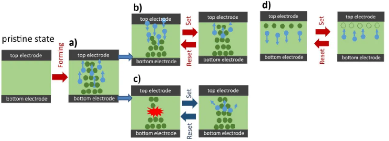
Due to the materials used we are primarily interested in oxygen ion migration effects. In which the application of voltage to an insulating oxide layer will cause oxygen ions to drift. These mechanisms can be divided into filamentary and area dependent.
In the filamentary mechanism the device starts in a pristine state without memristive behaviour, the application of voltage leads to the formation of filament along preexisting defects/impurities, 2.3 a. The device can then be bipolar, 2.3 b, in with voltage in the opposite polarity destroys the filament trough valence change. Or unipolar, 2.3 c, in with a high voltage in the same polarity destroys the filament trough joule heating. The filament can then be reformed by applying voltage in the same polarity as the initial electroforming. However, since the filament is never fully destroyed the voltage required is significantly lower.
In the area dependent mechanism the application of voltage leads to a general move-ment of oxygen ions an a change in overall resistance, the opposite polarity reverses the
2 . 2 . M E M R I S T O R S
Figure 2.2: Several possible mechanisms for reversible resistive switching.
process, 2.3 d. An electroforming process in not required and the device is already in a memristor state form the pristine state. [6, 8, 9, 12]
Figure 2.3: a,b and c are filamentary devices. a) illustrates the electroforming step. b) illustrates a valence change device working (bipolar). c) illustrated a thermochemical device working (unipolar). d) Illustrates a an area dependent bipolar device based on oxygen ion migration. [12]
By changing the area of the device and manipulating the insulating layer’s symmetry stoichiometry and composition the overall resistance, hysteresis and switching mecha-nism can be modified. Furthermore, by creating different contacts and changing the number of defects in the metal-insulator’s interface the memristor’s response can be manipulated.
C H A P T E R 2 . S TAT E O F T H E A R T
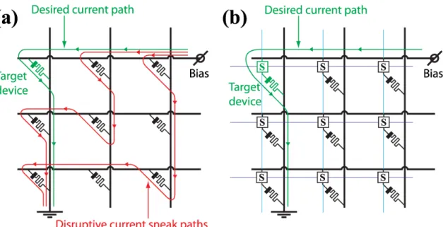
still be randomly accessible. Furthermore memristors can be fabricated at room temper-ature, compatible with back end of line processes required for 3D staking of multiple layers.[13] It is therefore advantageous to use a 3D device structure such as crossbar-arrays where the insulator is sandwiched between an array of metal contacts as seen in Figure 2.4, however this structure will cause sneak path currents and requires a selec-tor.[14, 15]
Figure 2.4: a) is an illustration of a single memristor in crossbar configuration and b) is a AFM image of a crossbar array.[13]
2.2.2 HP Lab’s 2008 memristor
Although the memristor had been theorized by Chua [7] in 1970 , it was only in 2008 that a team at HP Lab managed to fabricate a device.[6] this device was based on TiO2as
an insulator an Pt as metal contacts in a MIM thin film configuration. The insulator was divided into 2 layers, a highly doped layer and a depleted layer. The oxygen vacancies behaved as positive ionic charges leading to high conductivity on the doped layer. The passage of current causes the ions to drift and the resistance to change.[6]
2.3
Digital and analog memristors
A digital memristor is characterized by a steep set and reset wherein surpassing a thresh-old voltage will trigger a almost instant switch from Low resistance state (LRS) to High resistance state (HRS). Meaning said memristor will only have 2 possible resistance states HRS and LRS. An analog memristor is characterized by a gradual reset or set, this graduality can be time/voltage dependent or time/current dependent [16]. This means the memristor can have multiple resistance states. It is also possible for a memristor to be mixed i.e. to have an analog reset and a digital set, or vice-versa. Generally digital memristors are preferred for memories for their quick response time, but a fast analog
2 . 4 . D I G I TA L M E M O R I E S
memristor could be used with an MLC approach leading to increased memory density. [17]
2.4
Digital memories
In the digital world the binary system is used, such that storage devices have two dis-tinct states, one for “1” and one for “0”. These storage devices can generally be volatile memories (Dynamic Random access memory (DRAM), Static Random access memory (SRAM)) which are fast but require constant power and refreshing to maintain data, and non-volatile memories (magnetic tapes, floppy disks, optical disks and currently mag-netic disks and flash). Although speed is still a sought after characteristic it is not as important as with volatile memories, the main attributes being retention time, reliability and bit density.
DRAM memories are based around a capacitor holding charge with a selector transis-tor in a 1-Transistransis-tor-1-Capacitransis-tor (1T1C). Reading these memories involves sensing the charge present in the capacitor, erasing the data present and requiring a rewrite after every read. Since current leakage cannot be totally eliminated and is in fact increasing with the decrease in transistor size, charge can only be maintained for a limited time before the memory cell has to be refreshed (i.e. rewritten). The general speed of current generation DRAM is <10 ns.[18, 19]
Flash memories are based on a 3 terminal transistor device with a charge trapping layer or floating gate (FG) and function by trapping electrons which in turn change the transistors on voltage, this design is reliable and has fast read speeds (when compared with competing non-volatile memories) however it faces several problems, such as slow write speeds and limited number of writes. Until now these problems have been solved through 3D staking, cashing and most of all miniaturization. But since the scalability of transistors has been approaching fundamental limits, further improvements will be hard to achieve. The general speed of current generation flash is around 50 us. [20]
Ultimately, due to the gap between both types of memories a hierarchical memory system has been developed to optimize the use of fast but scarce DRAM and abundant but slow flash memory. With the fundamental limits of shrinking transistors being reached, problems such as shorter data retention time, current leakage, lower sensing margins, and difficulties in producing 3D staked NAND Flash, new memory solutions are required. One possibility is using a different architecture where the memory and arithmetic unit are one and the same (such as neuromorphic memristor computer), another would be achieving a non-volatile memory with speeds comparable to current gen RAM. [21] This last one has been explored with the discovery of novel RAMs such as magnetic (MRAM), phase change (PRAM), ferroelectric (FeRAM) and resistive (ReRAM). [12, 22]
The most common application proposed for memristors has been memristor based Resistive RAM (ReRAM), which can combine the high speed of SRAM, high density of DRAM, low cost and the non-volatility of flash memories. [8, 23] The small size (4F2) and
C H A P T E R 2 . S TAT E O F T H E A R T
the ability to easily stack memristors allows for higher density memory arrays without the need to reduce the feature size, leading to cheaper and easier fabrication. In the case of SOPs, the memristors versatility can facilitate the construction of a fully independent SOPs since a memristor array would be less complex and smaller than a comparable flash memory array. A more advanced future application could be a high-density non-volatile ReRAM module replacing both flash and RAM storage.
2.5
Problems and solutions
Figure 2.5: a) a memristor array without selector. b) a memristor array with a selector this can require extra wires here is depicted the worst case scenario with 2 extra wires. [24]
For commercial use the sneak-path current is one of the main impediments to the implementation of ReRAM. Sneak-path current is the unintended current that flows trough cells in a LRS, and will cause the memory cell’s noise margins to be shrunken, see 2.5.
Preventing sneak path current would ideally be done by the Schottky diode since it adds no complexity while maintaining low power consumption and array size. This how-ever can only work with unipolar devices since a bipolar device will require a relatively large voltage/current in the reverse polarity to reset, causing an avalanche breakdown of the diode. Thin film Zener diodes have been reported [25, 26] but these add undue complexity to the fabrication process.
The simplest selector is therefore a transistor, essentially pitting a 1T1C against a 1T1M memory cell, theoretically a memristor should be capable of speeds in excess of capacitors. This approach however eliminates most of the size advantage from memristors and adds latency.
2 . 5 . P R O B L E M S A N D S O LU T I O N S
A different solution has been proposed by Zidan et al. [15] a selector circuit using 2M cells (memistor[27]). This approach uses a memristor as a selector and adds 3Rof f to the
sneak path current. Since memristors can be stacked this solves the sneak path current issue without decreasing array density and keeping the 3 contacts used by current 1T1C DRAM cells. [14, 28]
3
Materials and Methods
3.1
Mask for photolithography
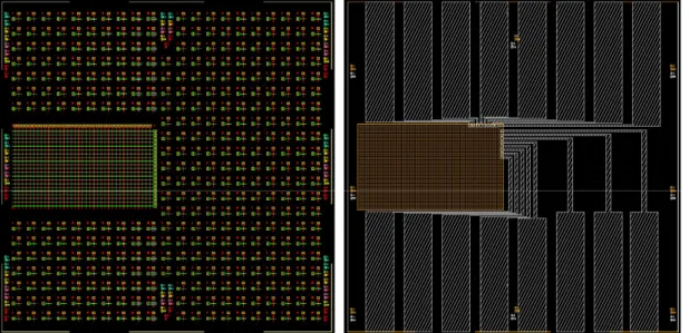
The following mask (Figure 3.2) was designed , using Cadence’s Virtuoso Layout Suite L. The basic device was designed with a crossbar configuration while ensuring that the contact pads were large enough for our characterization systems, with sizes ranging from 1 µm to 100 µm. The standard alignment marks used in CENIMAT were used. The mask is comprised of 2 sections: the individualized devices and the crossbar array. The individualized devices are composed by 3 layers: the bottom electrode (green), the active layer (blue) and the top electrode (red), see Figure 3.2c and Figure 3.1. Both the positive and negative masks were printed in order to allow choice of patterning methods and deposition materials. The final 3 layers were already optimized and were therefore printed in the required configuration, these are passivation layer (yellow) using parylene , insulation layer (orange) and a zip connector layer (white), see Figure 3.2b. These last two layers serve to isolate the crossbar array and to deposit contacts for testing part of the memristor array (8x8) for more complex systems. These last three layers were not used in this thesis, but were designed to be used for future device integration.
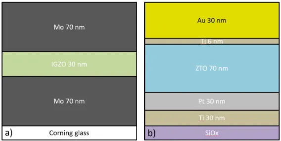
Figure 3.1: a) cross-section of the Mo-IGZO-Mo devices, b) cross-section of the Pt-ZTO-TiAu devices.
C H A P T E R 3 . M AT E R I A L S A N D M E T H O D S
a) 4 layers: top layer (red), middle (active) layer (blue), bottom layer (green) and passivization layer (yellow).
b) Insulator layer (orange), zipper layer (white) connects array with large zipper pads.
c) Zoomed image of individualized devices
Figure 3.2: Mask design
3 . 2 . D E V I C E FA B R I C AT I O N
3.2
Device fabrication
Several types of MIM devices were fabricated. In the following sections patterned devices, based on TiAu and Mo-IGZO-Mo, and non-pattern devices, based on Pt-ZTO-TiAu, will be presented. The devices based on Pt-ZTO-TiAu where fabricated on a silicon substrate coated with SiO2, for improved Pt adhesion. While the devices based on
Mo-IGZO-Mo where fabricated on Corning glass.
3.2.1 Thin film depositions
Before deposition the substrates were cleaned with two ultrasound baths. first in acetone for 10 minutes, and then in isopropyl for 10 minutes, they were then rinsed in water and dried with compressed N2.
E-beam evaporation (homemade apparatus) was used to deposit Pt and Au using Ti as an adhesion layer, with the conditions described in Table 3.1.
Table 3.1: Deposition conditions of e-beam depositions. Material Deposition pressure Current Deposition rate
Ti 10−6mBar 0.08 A 0.96 nm/min
Pt 10−6mBar 0.15 A 1.00 nm/min
Au 10−6mBar 0.08 A 1.50 nm/min
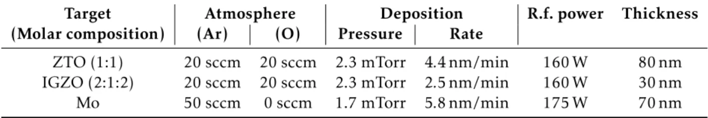
A sputtering system (AJA ATC-1800) was used to deposit ZTO, IGZO, Mo and to oxidize the Mo bottom layers. All depositions were done without intentional substrate heating, with a substrate distance to target of 35 cm. All targets were procured from AJA International, Inc. with 99.9% purity. The ZTO and IGZO targets had a diameter of 5.08 cm and the Mo target had a diameter of 7.62 cm. The conditions specific to each deposited material are described in Table 3.2.
Table 3.2: Deposition conditions of sputtering depositions.
Target Atmosphere Deposition R.f. power Thickness
(Molar composition) (Ar) (O) Pressure Rate
ZTO (1:1) 20 sccm 20 sccm 2.3 mTorr 4.4 nm/min 160 W 80 nm IGZO (2:1:2) 20 sccm 20 sccm 2.3 mTorr 2.5 nm/min 160 W 30 nm
Mo 50 sccm 0 sccm 1.7 mTorr 5.8 nm/min 175 W 70 nm
A plasma treatment in an atmosphere of oxygen (20 sccm) with a pressure of 20 mTorr, an r.f. power of 40 W and a substrate bias of 10 W was used for 15 min in order to oxidize the bottom contact of Mo before IGZO deposition.
C H A P T E R 3 . M AT E R I A L S A N D M E T H O D S
3.2.2 Patterning
The non-pattern devices (or bulk devices) only require one shadow mask (Annex A) for the top electrode which is a circle. Several sizes were produced but only results from the devices with a diameter of 700 µm will be presented.
The patterned devices were patterned using the mask shown in Figure 3.2, for the Ti-Pt, Ti-Au and ZTO layers lift off was used. The Mo was patterned using dry etching with SF6as etching gas and the IGZO was patterned by wet etching with a 1:20 solution of HCl:H2O. Although there are several sizes of patterned devices ranging from 1 µm of
square size to 100 µm.
3.3
Device characterization
3.3.1 XPS analysis
An X-ray photoelectron spectroscopy (XPS) depth profile was performed on an non-patterned Mo-IGZO-Mo device to confirm the IGZO stoichiometry and the formation of MoOx. The device was etched using a 500 atom argon cluster mode with a 10 eV
accelerating voltage rastered over am area of 1.5x1.5 mm2. 100 s etching steps were used. Between steps XPS analysis was performed using a Kratos Axis Supra with: a monochro-matic AlKα x-ray source at 300 W power, with an aperture of 110 µm and 40 eV pass energy.
3.3.2 Electrical DC characterization
Electrical characterization was performed using three semiconductor characterization systems:
Keithley 4200SCS connected to an electrically isolated probe station (Janis ST-500), both TE and BE were connected to source measure units (SMU).
Agilent HP 4155C connected to BE and TE via an isolated probe station (Cascade M150).
Keysight B1500A connected to BE and TE via an isolated probe station (Cascade EPS150 Triax).
The following device characteristics were investigated: pristine state, set , reset, oper-ation window, retention, analog reset, cycling, set and reset speed, pulsed operoper-ation.
If the pristine state is in a low resistance state, then a device initialization/electro-forming step might be necessary to achieve a memory, this step was done by applying a voltage sweep starting and ending at 0 V. A current compliance (CC) is used in order to minimize stress on the devices, CC is set at the lowest possible value, and the sweep is increased until a set is achieved.
Set and reset voltages and currents were investigated. After an electroforming/ini-tialization process set and reset were repeated to ascertain the reliability and discover
3 . 3 . D E V I C E C H A R AC T E R I Z AT I O N
the best voltage and CC settings. This was followed by a study of the Ron/of f ratio and
retention capabilities of the device by applying a constant voltage of 0.1V and measuring current for up to 1000 seconds. Analog operation was also explored by attempting to achieve intermediate resistance states between HRS and LRS. This was done in the reset by applying successively larger voltage sweeps.
3.3.3 Electrical pulse characterization
A Keysight wave generator was used in series with the device and (Keithley 4200SCS) via a probe station (Janis). The Keysight 33522A Function (Arbitrary Waveform Generator) generated pulses and Keithley was used to measure the current. The wave generator was used to increase the pulse speed. The pulses were set up to have a high set/reset value and a low read value of 0.1 V, the pulse width was varied between 1 s down to the wave generators limit of 10 ns. Between pulse tests transient set and reset was done in order to ensure that the starting point is as similar as possible. Once set and reset speeds had been determined, full set and reset cycles were done using only pulses.
4
Results
4.1
Non-patterned Pt-ZTO-TiAu memristors
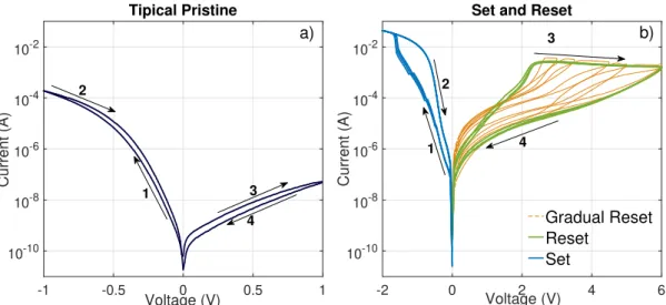
Figure 4.1a shows a typical pristine state for a functioning Pt-ZTO-TiAu device, which showed reasonable rectification. A large Ron/of f ratio was achieved such as in Figure 4.1b.
The stop-voltage method was used to achieve a gradual reset. This consists in applying successive DC sweeps while increasing the sweep voltage range. This is a replication of behaviour reported in [29]. While most devices had a digital set and analog reset, other Pt-ZTO-TiAu devices with different properties where found, with the main combinations being fully digital, fully analog and digital set with analog reset, these properties could be controlled by an electroforming/initialization step. However, this is a complex step and the exact electrical characteristics are still an open question. Retention and cycling was tested on the smaller patterned devices since smaller have increased performance and stability. Due to large area and contamination by dust particles the device yield was very low therefore further reducing the device size and the potential for contamination is required. -1 -0.5 0 0.5 1 Voltage (V) 10-10 10-8 10-6 10-4 10-2 Current (A) Tipical Pristine -2 0 2 4 6 Voltage (V) 10-10 10-8 10-6 10-4 10-2 Current (A)
Set and Reset
Gradual Reset Reset Set 1 2 3 4 1 2 3 4 a) b)
Figure 4.1: a) Typical pristine state, showing some rectification b) Digital set and analog reset for non-patterned device.
C H A P T E R 4 . R E S U LT S
4.2
Patterned Pt-ZTO-TiAu memristors
4.2.1 Set and reset
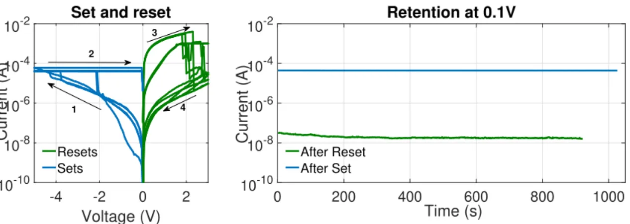
As we can see in Figure 4.2a set and reset are both digital, although the Ron/of f ratio is
quite large (>103), the set and reset voltages are erratic, furthermore uniformity between devices is very low. There is no rectification on the HRS but there is some rectification on the LRS, however this rectification is still too weak to prevent the sneak path current in an crossbar array of significant size [14, 15], as well as it being unstable and not always present. After some cycles, retention was measured for ∼1000 seconds after set as well as after reset, see Figure 4.2b. This is in accordance with previous results which have tested retention more extensively.[30] So far, these devices have proven to be functional as ReRAM however some problems exist: the lack of rectification will require a selector to be added to the final array reducing speed and the Ron/of f ratio, increasing complexity
and possibly decreasing bit density. While the instability is concerning and should be reduced if possible, since the Ron/of f ratio is so large, it should not impair the functioning
of the device. A way to improve the final system would be to increase the bit density of individual memristors, this will be explored in the next section.
-4 -2 0 2 Voltage (V) 10-10 10-8 10-6 10-4 10-2 Current (A)
Set and reset
Resets Sets 0 200 400 600 800 1000 Time (s) 10-10 10-8 10-6 10-4 10-2 Current (A) Retention at 0.1V After Reset After Set 4 2 3 1
Figure 4.2: a) Digital set and reset for a patterned 5 µm squared device , CC of 5/8 × 10−
5 A was used and b) retention at 0.1 V for ∼1000 s
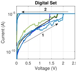
4.2.2 Gradual reset and digital set
As stated previously gradual operation allows for multiple bits per cell (MLC approach) and it can also provide more precise control over resistance and has novel applications in IC design[31]. While we are still using the same devices, they can behave in a gradual manner. This can sometimes be determined by the initial step of electroforming/initial-ization. However this is a complex step and is not reliable, requiring further investigation. Instead of starting form a pristine state with high resistivity, a pristine device already in a LRS was found. Upon applying a initialization step, a gradual reset with switched polar-ity was achieved, see Figure 4.4 while the set remained digital, see Figure 4.3. Since the
4 . 2 . PAT T E R N E D P T- Z T O -T I AU M E M R I S T O R S
polarity was reversed we would expect a filamentary behavior, however this was incon-clusive.[29] With a gradual reset, an MLC approach using the stop voltage method was explored. While enough levels for 3 bit operation could be achieved, it is clear that the instability of the device can no longer be masked by its large Ron/of f ratio, see Figure 4.4.
It is possible that a 2 bit cell could be achieved with the current device.
0 0.5 1 1.5 2 2.5 Voltage (V) 10-10 10-5 Current (A) Digital Set 2 1
Figure 4.3: Digital set with a CC of 1×10−
5 A
4.2.3 Pulse speed testing and operation
After confirming that the memristor was functional (Figure 4.5) 1V pulses were applied, followed by a DC sweep sets. Initially only resets were tried since our setup did not allow for CC during pulsed operation. Starting with 100us pulses the pulse width was reduced until there was no reset. Then the pulse width was raised to determine the threshold at which the reset happened. This was determined to be 100ns, see Figure 4.6. This timing was remarkably abrupt with even 99ns width pulses not having any effect. This is still much higher than the theoretical speed limit discussed in Menzel et al. around 85 ps [32], so it is likely we could be limited by our measurement setup which has an operating frequency around 15MHz and that reducing the device’s size could help improve its speed. Nevertheless, this falls closer to DRAM speeds than to Flash while still being non-volatile and having a much higher density than DRAM.
Following the speed tests a series of set and reset using only pulses were done. Again as with transient cycling, the device had a very large Ron/of f ratio, with this specific device
larger voltages were required to maintain the 100ns switching speed. Due to our setup cylcing with pulses was not possible. Its likely that using pulses will extend the life time of the device.
To study current density, the current was measured at 0.1 V and -0.1 V with devices of all available sizes, see Annex B. All size showed rectification with the smaller devices being better. The current density was not stable between sizes, there is also a large error margin.
C H A P T E R 4 . R E S U LT S -2 -1.5 -1 -0.5 0 Voltage (V) 10-10 10-8 10-6 10-4 10-2 Current (A) Initialization -1.5 -1 -0.5 0 Voltage (V) 10-10 10-8 10-6 10-4 10-2 Current (A) Gradual Resets 4 resets 2 resets 4 resets -2 -1.5 -1 -0.5 0 Voltage (V) 10-10 10-8 10-6 10-4 10-2 Current (A) Gradual Reset 1 First reset -0.7 V Last reset -1.6 V -2 -1.5 -1 -0.5 0 Voltage (V) 10-10 10-8 10-6 10-4 10-2 Current (A) Gradual Reset 2 First reset -0.7 V Last reset -2 V 2 1 2 1 1 1 2 2
a)
b)
c)
d)
Figure 4.4: a) Initialization from a device with high current pristine state, b) mulriple gradual reset with 5, 3 and 5 different states , c) and d) gradual reset with MLC approach.
-3 -2 -1 0 1 2 Voltage (V) 10-8 10-6 10-4 10-2 Current (A)
Set and reset
Set and reset
Sets after pulsed reset
1
4 3 2
Figure 4.5: Digital set and reset of the device used in the pulse speed testing, note that for speed testing set was initially done in transient.
There are 2 problems left when applying these memristors in real world applications: instability and the lack of rectification, which will cause sneak path current in arrays.
4 . 2 . PAT T E R N E D P T- Z T O -T I AU M E M R I S T O R S 0 10 20 30 40 50 Time (s) 10-10 10-5 100 Current (A) 0 500 1000 Time (us) 0 1 2 Voltage (V) 1 V 100 us 0 10 20 30 40 50 Time (s) 10-10 10-5 100 Current (A) 0 500 1000 Time (us) 0 1 2 Voltage (V) 1 V 50 us 0 10 20 30 40 50 Time (s) 10-10 10-5 100 Current (A) 0 500 1000 Time (ns) 0 1 2 Voltage (V) 1 V 100 ns 0 10 20 30 40 50 Time (s) 10-10 10-5 100 Current (A) 0 500 1000 Time (ns) 0 1 2 Voltage (V) 1 V 50 ns 0 10 20 30 40 50 Time (s) 10-10 10-5 100 Current (A) 0 500 1000 Time (ns) 0 1 2 Voltage (V) 1 V 75 ns 0 10 20 30 40 50 Time (s) 10-10 10-5 100 Current (A) 0 500 1000 Time (ns) 0 1 2 Voltage (V) 1 V 90 ns 0 10 20 30 40 50 Time (s) 10-10 10-5 100 Current (A) 0 500 1000 Time (ns) 0 1 2 Voltage (V) 1 V 100 ns 0 10 20 30 40 50 Time (s) 10-10 10-5 100 Current (A) 0 500 1000 Time (ns) 0 0.5 1 1.5 2 Voltage (V) 1 V 95 ns 0 10 20 30 40 50 Time (s) 10-10 10-5 100 Current (A) 0 500 1000 Time (ns) 0 1 2 Voltage (V) 1 V 99 ns 0 10 20 30 40 50 Time (s) 10-10 10-5 100 Current (A) 0 500 1000 Time (ns) 0 1 2 Voltage (V) 1 V 100 ns
Figure 4.6: Reset speed test, pulses are divided into 2 plots each, a top one with readout current at 0.1 V and a bottom one with the input 1 V pulse, from left to right there is 100us, 50us, 100ns, 10ns, 75ns and 90ns, 100ns, 95ns, 99ns and 100ns.
0 50 Time (s) 10-10 10-5 100 Current (A) Reset 0 500 1000 Time (ns) 0 5 Voltage (V) 0 50 Time (s) 10-10 10-5 100 Current (A) Set 0 500 1000 Time (ns) -4 -2 0 Voltage (V) 0 50 Time (s) 10-10 10-5 100 Current (A) Set 0 500 1000 Time (ns) -4 -2 0 Voltage (V) 0 50 Time (s) 10-10 10-5 100 Current (A) Reset 0 500 1000 Time (ns) 0 5 Voltage (V) 0 50 Time (s) 10-10 10-5 100 Current (A) Reset 0 500 1000 Time (ns) 0 5 Voltage (V) 0 50 Time (s) 10-10 10-5 100 Current (A) Set 0 500 1000 Time (ns) -5 0 5 Voltage (V) 0 50 Time (s) 10-10 10-5 100 Current (A) Reset 0 500 1000 Time (ns) 0 5 Voltage (V)
Figure 4.7: Set and reset done entirely with pulses, pulses are divided into 2 plots the top one is readout current at 0.1 V and the bottom one represents the applied pulse.
Instability will improve in industrial production and by the reduction of the feature size into the nanometer scale, furthermore when competing with the limited capacities of DRAM, multi-bit operation is not critical so a 1-bit memristor cell can be used. The solutions to the sneak path current have already been discussed.
4.2.4 Current sweep
The Pt-ZTO-TiAu devices with digital operation have a current controlled set, therefore by using a voltage sweep they are not being controlled since the current will have some randomness. Furthermore, using voltage sweep once a certain threshold is surpassed the memristor snaps to the LRS, hence the necessity for a CC, this invariably leads to over-stressing of the device. A current sweep approach allows for a more precise control of current and for more data points to be gathered in the jump area. In Figure 4.8 we can observe that once the set switching begins it continues at a constant voltage. This
C H A P T E R 4 . R E S U LT S
approach allowed us to test devices of larger sizes without burning and could be a solution to the low yield ans high variability seen in 4.2. However further study is required.
-1 -0.5 0 0.5 1 Voltage (V) 10-10 10-8 10-6 10-4 Current (A)
Pristine state diode-type (voltage sweep)
100 µm 80 µm 50 µm 40 µm 30 µm -4 -3 -2 -1 0 Voltage (V) 0 0.5 1 1.5 2 Current (A) ×10-4 Current sweep 100 µm 50 µm 40 µm 30 µm
Figure 4.8: The first graph is the pristine state of several devices, the second graph shows the electroforming process using current sweep for some devices of different sizes. [6]
4.3
Patterned Mo-IGZO-Mo memristors
4.3.1 Pristine state, set and reset
Unlike Pt-ZTO-TiAu devices, Mo-IGZO-Mo devices were more stable and had high unifor-mity between devices. Figure 4.9 shows the typical pristine state. There is some rectifying behavior, especially for the lower read voltages (<0.4 V) which is the intended effect of the plasma treatment. Since the MoO3has a much higher work function than Mo, a barrier is
created between the MoO3and IGZO, therefore, allowing for the replacement of Pt with Mo. [33] After the initialisation step, shown in Figure 4.10 in red, the diode-like device shows high reverse current. This can be optimized further in processing, or require the use of selectors in arrays of any significant size. After initialization the device is rather stable, with both set and reset being analog, this however comes at a cost of a very small
Ron/of f ratio, which nullifies the main advantage of analog operation, MLC, since the
Ron/of f ratio is too small to contain more than 2 resistance levels. The set and reset are
analog with an asymmetrical shape and some rectifying behavior this is indicative of a area-dependent ion migration mechanism at the interface. [12]
4 . 3 . PAT T E R N E D M O - I G Z O - M O M E M R I S T O R S -1 -0.5 0 0.5 1 Voltage (V) 10-12 10-10 10-8 10-6 Current (A) Pristine diode
Figure 4.9: Pristine state for the IGZO devices, with pronounced rectification.
-2.5 -2 -1.5 -1 -0.5 0 0.5 1 1.5 2 2.5 Voltage (V) 10-8 10-6 10-4 Current (A)
Initialization, Set and Reset
Initialization Sets Resets 1 2 3 4
Figure 4.10: Initialization and analog set and reset.
An XPS depth profile was performed, however it was not possible to identify the MoOx. Likely due to it being too thin or due to the reductive action of the Ar beam
used for the etching. The XPS analysis, seen in 4.11, confirms the device structure, the stoichiometry present in the target was not transferred to the device, this was expected and the reduced Zn ratio as been previously shown [34]. However, the stoichiometry of the IGZO layer also changed along the thickness of the layer, this was not expected and might be due to uneven heating of the target. This structure is generally associated with a oxygen migration mechanisms, but a more in-depth analysis with measurements at HRS and LRS would be necessary for confirmation.
In order to study area dependency of current, set and reset cycles were done in several devices of different sizes and the highest current on the reset side was measured and averaged over 3 cycles, 4.12 exemplifies the curves for devices with square sizes of 2 µm and 20 µm. 4.13 shows the current measured and the areas of different devices, there
C H A P T E R 4 . R E S U LT S 0 500 1000 1500 2000 2500 3000 3500 Etch time (s) 0 10 20 30 40 50 60 70 80 90 100 Atomic Concentration (%) XPS depth profile Ga 2p In 3d Mo 3d O 1s Zn 2p
a) A depth profile of one device, showing the MIM structure. 1000 1500 2000 2500 Etch time (s) 0 1 2 3 4 5 Atomic fraction
IGZO ratio with etch time
Ga In Zn
b) Using the data from the XPS profile and as-suming the Zn remains constant the relative ra-tios of In and Ga were calculated.
Figure 4.11: XPS depth profile. We can observe the change in ratio along the depth, this is typical of homogeneous oxygen migration mechanisms. [12]
is a clear linear relationship between current and area with a current density around 105A/m2, this confirms our assertion that the mechanism at play is surface uniform ion migration and therefore area-dependent.
0 0.5 1 1.5 2 2.5 Voltage (V) 10-10 10-8 10-6 10-4 Current (A)
Reset for 4 µm and 400 µm
1
2
1
2 4 µm
40 µm
Figure 4.12: Reset for devices with square sizes of 2 um and 20 um. The arrows indicate the curve zone used for measuring the current.
4 . 3 . PAT T E R N E D M O - I G Z O - M O M E M R I S T O R S 10-12 10-11 10-10 10-9 10-8 Area (m2) 10-7 10-6 10-5 10-4 10-3 Current (A)
Current variation with device size
10-12 10-11 10-10 10-9 10-8 Area (m2) 103 104 105 106 107
Current density (A/m
2 )
Current density variation with device size b) a)
Figure 4.13: a) Current variation with device area and b) Current density variation with size, as can be seen there is a clear linear relation between current and area.
4.3.2 Cycling and retention
100 cycles of set and reset inter-spaced with 250 seconds of retention were performed on a device. Initially there is some instability, however after some cycles the set and reset levels stabilize, with very little decay, see Figure 4.14. The movement of the states upward is indicative of a charging phenomenon.
-2 -1 0 1 2 Voltage (V) 10-10 10-8 10-6 10-4 Current (A)
Set and Reset 100 cycles
Cycle 1 Cycle 50 Cycle 100 0 50 100 150 200 250 Time (s) 10-8 10-7 10-6 Current (A) Retention 100 cycles at 0.1 V Cycle 1 Cycle 50 Cycle 100 1 4 3 2
Figure 4.14: Set and reset cycling and retention states.
The retention data was used to calculate the cumulative distribution function (Cdf) which confirms our analysis that both set and reset states are stable and drifting to higher currents, see Figure 4.15.
C H A P T E R 4 . R E S U LT S 10-8 10-7 10-6
Current (A)
0 20 40 60 80 100 Cdf (%)Cdf - Set
10-8 10-7 10-6Current (A)
0 20 40 60 80 100 Cdf (%)Cdf - Reset
Figure 4.15: Cdf of 100 cycles after set and reset 4.3.3 Pulsed speed and operation
The Mo-IGZO-Mo devices operation is fully analog, therefore there isn’t a definite pulse speed, set and reset begin with 10 ms pulse width and continue until 1 s pulse width, see ( Figure 4.16). Since 2 s pulses only improved the Ron/of f ratio marginally 1 s pulses were chosen. Higher voltages were tried in order to reduce the pulse width, however the voltage level quickly rose above what the devices could sustain, burning the devices. The Pt-ZTO-TiAu devices which could sustain similar voltages in transient operation, could sustain higher pulse voltages (up to 6V, Figure 4.7) likely due to the very short pulse widths used. Higher voltages were used for reset to improve the Ron/of f ratio but
symmetric cycles were also done.
Using a different 5 µm device, cycles using 1 s pulses and 100 s retention time at 0.1 V were performed. Over 500 cycles were performed on the same device. The Cdf can be seen in 4.17. There is a very low error and no drift in the states.
Unlike the DC sweep cycles in 4.3.2 there is no appreciable change in the HRS and LRS as can be seen in 4.18a and 4.18b, i.e.:there is no charging phenomenon. However there is still a stabilization of the states, therefore some stabilization loops might be required.
The average HRS was 25 ± 1 nA and the average LRS was 43 ± 2 nA this window is very small. Optimizing this window of operation and improving the device’s for speed is necessary. The same problems and solutions regarding sneak-path current outlined in 4.2.3 apply, excepting that in this case the selecting memristor would have to be different seeing as this must have a large Ron/of f ratio.
4 . 3 . PAT T E R N E D M O - I G Z O - M O M E M R I S T O R S Set 10 20 30 40 50 Time (s) 10-9 10-8 Current (A) Reading at 0.1 V 0 5 10 Time (s) -1.5 -1 -0.5 0 0.5 Voltage (V) Pulses 1 s 10 20 30 40 50 Time (s) 10-9 10-8 Current (A) 0 500 1000 Time (ms) -1.5 -1 -0.5 0 0.5 Voltage (V) 100 ms 0 10 20 30 40 50 60 Time (s) 10-9 10-8 Current (A) 450 500 550 Time (ms) -1.5 -1 -0.5 0 0.5 Voltage (V) 10 ms Reset 10 20 30 40 50 Time (s) 10-9 10-8 Current (A) Reading at 0.1 V 0 5 10 Time (s) 0 0.5 1 1.5 2 Voltage (V) Pulses 1 s 10 20 30 40 50 Time (s) 10-9 10-8 Current (A) 0 500 1000 Time (ms) 0 0.5 1 1.5 2 Voltage (V) 100 ms 0 10 20 30 40 50 60 Time (s) 10-9 10-8 Current (A) 450 500 550 Time (ms) 0 0.5 1 1.5 2 Voltage (V) 10 ms
Figure 4.16: Testing pulse speed with Mo-IGZO-Mo device, reading at 0.1 V with Keithley in blue and pulse generated by Keysight wave generator in orange, arrows indicate a pulse. From top to bottom : set 1 s, 100 ms and 10 ms width pulses at -1 V, reset 1 s, 100 ms and 10 ms width pulses at 1.5 V.
C H A P T E R 4 . R E S U LT S 2 4 6 8 10 Current (A) ×10-8 0 20 40 60 80 100 Cdf (%) Cdf HRS LRS
Figure 4.17: Cdf of 300 cycles (first 150 and last 150 cycles).
2 4 6 8 10 Current (A) ×10-8 0 20 40 60 80 100 Cdf (%) Comparing Cdf First 150 First 150 Last 150 Last 150 HRS LRS
a) Comparing Cdfs of the first 150 cycles (darker) whit the last 150 cycles (lighter).
0 1 2 3 Time (s) ×104 10-8 10-7 Current (A) Pulsed cycling First 150 First 150 Last 150 Last 150 LRS HRS
b) Comparing the average value of the retention time.
Figure 4.18: Comparison between the first 150 cycles (darker) and the last 150 cycles (ligther).
5
Conclusions and future
prospects
5.1
Conclusions
Pt-ZTO-TiAu based memristors were shown to function with large Ron/of f (>103), the
switching mechanism seems to be filamentary based although further research is required. Although the main mechanism seems to be valence change, several confounding effects could be interfering, such as charge trapping effects and other electronic effects. This purely filamentary behavior seems to be linked with size since the larger non-patterned devices looked area-dependent. Such a device and mechanism is clearly suited to ReRAM applications. Due to its filamentary nature, further reductions in size are unlikely to increase operating speed or decrease power consumption, while increasing reliability.
Mo-IGZO-Mo based memristors were shown to function reliably and during large cycles. The switching mechanism was identified as homogeneous oxygen ion migration at the surface and is therefore area dependent. Although this mechanism can be suited for ReRAM our devices are not, due to slow operation and small Ron/of f ratio. A better
use could be neuromorphic computing or alternative logic circuits. Further decreases in size can improve operating speed and reduce power consumption.
5.2
Future prospects
For Pt-ZTO-TiAu devices one should increase the stability and optimize the fabrication process by improving the patterning and the smoothness of the layers. Furthermore it would be interesting to do pulsed cycling, temperature testing, and study the area dependency after the initialization/electroforming process.
For the Mo-IGZO-Mo devices one should increase speed and Ron/of f. Again, testing
cycles with temperature would be interesting.
Furthermore, optimizing a device without Pt, Au and IGZO which are rare and more expensive should be tried, further miniaturizing the devices should also help achieve these objectives. Finaly the sneak-path current, in a crossbar array should be studied and the solutions outlined should be implemented.
Bibliography
[1] H. Iwai, “End of the downsizing and world after that,” Proceedings - 2017 4th International Conference on Mathematics and Computers in Sciences and in Industry, MCSI 2017, pp. 138–143, 2017. d o i: 10.1109/MCSI.2017.32.
[2] J. Seok, W.-j. Maeng, H.-s. Kim, and J.-s. Park, “Review of recent developments in amorphous oxide semiconductor thin-film transistor devices,”Thin Solid Films,
vol. 520, no. 6, pp. 1679–1693, 2012. d o i: 10.1016/j.tsf.2011.07.018.
[3] B. R. A. Street, “Thin-film transistors,”Advanced Materials, vol. 21, no. 20, pp. 2007–
2022, 2009. d o i: 10.1002/adma.200803211.
[4] A. Facchetti and T. J. Marks,Transparent electronics : from synthesis to applications.
Wiley, 2010, p. 448, i s b n: 0470710594.
[5] P. Görrn, M. Sander, J. Meyer, M. Kröger, E. Becker, H.-H. Johannes, W. Kowalsky, and T. Riedl, “Towards see-through displays: Fully transparent thin-film transis-tors driving transparent organic light-emitting diodes,”Advanced Materials, vol. 18,
no. 6, pp. 738–741, 2006. d o i: 10.1002/adma.200501957.
[6] D. B. Strukov, G. S. Snider, D. R. Stewart, and R. S. Williams, “The missing memristor found,” Nature, vol. 453, no. 7191, pp. 80–83, 2008. d o i: 10 . 1038 /
nature06932.
[7] L. O. Chua, “Memristor—The Missing Circuit Element,”IEEE Transactions on Cir-cuit Theory, vol. 18, no. 5, pp. 507–519, 1971. d o i: 10.1109/TCT.1971.1083337.
eprint: TCT.1971.1083337 (10.1109).
[8] J. Rosa, A. Kiazadeh, L. Santos, J. Deuermeier, R. Martins, H. L. Gomes, and E. For-tunato, “Memristors using solution-based igzo nanoparticles,”ACS Omega, vol. 2,
no. 11, pp. 8366–8372, 2017. d o i: 10.1021/acsomega.7b01167.
[9] Z. Q. Wang, H. Y. Xu, X. H. Li, H. Yu, Y. C. Liu, and X. J. Zhu, “Synaptic learning and memory functions achieved using oxygen ion migration/diffusion in an amorphous ingazno memristor,”Advanced Functional Materials, vol. 22, no. 13, pp. 2759–2765,
2012. d o i: 10.1002/adfm.201103148.
[10] J. S. Rajachidambaram, S. Murali, J. F. Conley, S. L. Golledge, and G. S. Herman, “Bipolar resistive switching in an amorphous zinc tin oxide memristive device,”
Journal of Vacuum Science & Technology B, vol. 31, no. 1, 01A104, 2013. d o i: 10.
B I B L I O G R A P H Y
[11] B. Lu, Y. Lu, H. Zhu, J. Zhang, S. Yue, S. Li, F. Zhuge, Z. Ye, and J. Lu, “Memristors based on amorphous znsno films,”Materials Letters, vol. 249, pp. 169 –172, 2019,
i s s n: 0167-577X. d o i: https://doi.org/10.1016/j.matlet.2019.04.086. [12] S. Slesazeck and T. Mikolajick, “Nanoscale resistive switching memory devices: A
review,” Nanotechnology, vol. 30, no. 35, p. 352 003, 2019. d o i:
10.1088/1361-6528/ab2084.
[13] P. Lin and Q. Xia, “Tutorial: Fabrication and three-dimensional integration of nanoscale memristive devices and arrays,” Journal of Applied Physics, vol. 124,
no. 15, p. 152 001, 2018. d o i: 10.1063/1.5038109. [Online]. Available: http: //aip.scitation.org/doi/10.1063/1.5038109.
[14] F. Gül, “Addressing the sneak-path problem in crossbar RRAM devices using memristor-based one Schottky diode-one resistor array,”Results in Physics, vol. 12,
pp. 1091–1096, Mar. 2019. d o i: 10.1016/j.rinp.2018.12.092.
[15] M. A. Zidan, H. A. H. Fahmy, M. M. Hussain, and K. N. Salama, “Memristor-based memory: The sneak paths problem and solutions,”Microelectronics Journal, vol. 44,
no. 2, pp. 176–183, 2013. d o i: 10.1016/j.mejo.2012.10.001.
[16] S. Samanta, D. S. Z. Rahaman, A. Roy, S. Jana, S. Chakrabarti, R. Panja, S. Roy, M. Dutta, S. Ginnaram, A. Prakash, S. Maikap, H.-M. Cheng, L.-N. Tsai, J.-T. Qiu, and S. Ray, “Understanding of multi-level resistive switching mechanism in geox through redox reaction in h2o2/sarcosine prostate cancer biomarker detection,”
Scientific Reports, vol. 7, Dec. 2017. d o i: 10.1038/s41598-017-11657-4.
[17] J. Deuermeier, A. Kiazadeh, A. Klein, R. Martins, and E. Fortunato, “Multi-Level Cell Properties of a Bilayer Cu2O/Al2O3 Resistive Switching Device,” Nanomateri-als, vol. 9, no. 2, p. 289, 2019. d o i: 10.3390/nano9020289.
[18] K. C. Chun, W. Zhang, P. Jain, and C. H. Kim, “A 2t1c embedded dram macro with no boosted supplies featuring a 7t sram based repair and a cell storage monitor,”
IEEE Journal of Solid-State Circuits, vol. 47, no. 10, pp. 2517–2526, 2012. d o i: 10.
1109/JSSC.2012.2206685.
[19] C. H. Cheng and A. Chin, “Low-leakage-current dram-like memory using a one-transistor ferroelectric mosfet with a hf-based gate dielectric,”IEEE Electron Device Letters, vol. 35, no. 1, pp. 138–140, 2014. d o i: 10.1109/LED.2013.2290117.
[20] K. Takeuchi, T. Tanaka, and T. Tanzawa, “A multipage cell architecture for high-speed programming multilevel nand flash memories,”IEEE Journal of Solid-State Circuits, vol. 33, no. 8, pp. 1228–1238, 1998. d o i: 10.1109/4.705361.
[21] S. K. Park, “Technology scaling challenge and future prospects of dram and nand flash memory,”2015 IEEE International Memory Workshop (IMW), pp. 1–4, 2015.
d o i: 10.1109/IMW.2015.7150307.
B I B L I O G R A P H Y
[22] A. Chen, “A review of emerging non-volatile memory (nvm) technologies and ap-plications,” Solid-State Electronics, vol. 125, pp. 25 –38, 2016, Extended papers
selected from ESSDERC 2015. d o i: https://doi.org/10.1016/j.sse.2016.07. 006.
[23] J. J. Yang, D. B. Strukov, and D. R. Stewart, “Memristive devices for computing,”
Nature Nanotechnology, vol. 8, no. 1, pp. 13–24, 2013. d o i: 10.1038/nnano.2012.
240.
[24] R. Berdan, A. Serb, A. Khiat, A. Regoutz, C. Papavassiliou, and T. Prodromakis, “A µ -controller-based system for interfacing selectorless rram crossbar arrays,”
IEEE Transactions on Electron Devices, vol. 62, no. 7, pp. 2190–2196, 2015, i s s n:
1557-9646. d o i: 10.1109/TED.2015.2433676.
[25] T. Cassagneau, T. E. Mallouk, and J. H. Fendler, “Layer-by-layer assembly of thin film zener diodes from conducting polymers and cdse nanoparticles,”Journal of the American Chemical Society, vol. 120, no. 31, pp. 7848–7859, 1998. d o i: 10.1021/
ja9806027.
[26] P. Van Dorpe, Z. Liu, W. Van Roy, V. F. Motsnyi, M. Sawicki, G. Borghs, and J. De Boeck, “Very high spin polarization in gaas by injection from a (ga,mn)as zener diode,”Applied Physics Letters, vol. 84, no. 18, pp. 3495–3497, 2004. doi: 10.1063/
1.1738515.
[27] S. P. Adhikari and H. Kim, “Why are memristor and memistor different devices?” In
Memristor Networks, A. Adamatzky and L. Chua, Eds. Cham: Springer International
Publishing, 2014, pp. 95–112. d o i: 10.1007/978-3-319-02630-5_6.
[28] Y. Chen, H. H. Li, W. Zhang, R. E. Pino, and S. Member, “The 3-D Stacking Bipolar RRAM for High Density,” vol. 11, no. 5, pp. 948–956, 2012. d o i: 10.1109/TNANO. 2012.2208759.
[29] N. M.d.A. C. Branca, “Memristor based on amorphous zinc-tin oxide schottky diodes,” Master’s thesis, 2019. d o i: 10362/75825.
[30] N. Branca, J. Deuermeier, J. Martins, E. Carlos, R. Martins, F. Elvira, and A. Ki-azadeh, “Two-dimensional resistive switching based on amorphous zinc-tin oxide schottky diodes.”
[31] M. A. Zidan, A. Chen, G. Indiveri, and W. D. Lu, “Memristive computing devices and applications,” Journal of Electroceramics, vol. 39, no. 1, pp. 4–20, 2017. d o i:
10.1007/s10832-017-0103-0.
[32] S. Menzel, M. von Witzleben, V. Havel, and U. Böttger, “The ultimate switching speed limit of redox-based resistive switching devices,”Faraday Discuss., vol. 213,
B I B L I O G R A P H Y
[33] Y. Guo and J. Robertson, “Origin of the high work function and high conductivity of moo3,”Applied Physics Letters, vol. 105, no. 22, p. 222 110, 2014. d o i: 10.1063/
1.4903538.
[34] A. Olziersky, P. Barquinha, A. Vilà, C. Magaña, E. Fortunato, J. Morante, and R. Mar-tins, “Role of ga2o3–in2o3–zno channel composition on the electrical performance of thin-film transistors,”Materials Chemistry and Physics, vol. 131, no. 1, pp. 512
–518, 2011, i s s n: 0254-0584. d o i: https://doi.org/10.1016/j.matchemphys. 2011.10.013. [Online]. Available: http://www.sciencedirect.com/science/ article/pii/S0254058411008571.
I
Annex
I.1
Annex A
Figure I.1: Shadow mask for deposition of top electrodes, the sizes are, from top to bottom 500 µm, 600 µm, 700 µm, 800 µm, 900 µm, 1000 µm.
A N N E X I . A N N E X
I.2
Annex B
10
-1110
-1010
-910
-8Area (m
2
)
10
-510
-410
-310
-210
-1Current density (A/m
2
)
Current density variation with device size
Reverse polarity
Forward polarity
Figure I.2: Current density variation with area of Pt-ZTO-TiAu memristors, as we can see the current density is not constant and there is no obvious relation. The higher currents for very large areas could be due to the increased probability of impurities. The instability of the devices prevented us from testing current densities in HRS and LRS and infer filamentary or area dependent behavior.
![Figure 2.4: a) is an illustration of a single memristor in crossbar configuration and b) is a AFM image of a crossbar array.[13]](https://thumb-eu.123doks.com/thumbv2/123dok_br/15705048.1067949/24.892.132.755.314.598/figure-illustration-single-memristor-crossbar-configuration-image-crossbar.webp)