1
Passivation of interfaces in thin film solar cells: understanding the effects of a
nanostructured rear point contact layer
P. M. P. Salomé1,2*, Bart Vermang3,4,5, R. Ribeiro-Andrade 1,6, J. P. Teixeira2, J. M. V. Cunha1,7, M. J. Mendes7, S. Haque7, J. Borme1, H. Aguas7, E. Fortunato7, R. Martins7, J. C. González6, J. P.
Leitão2, P. A. Fernandes1,8, M. Edoff9 and S. Sadewasser1
(1) International Iberian Nanotechnology Laboratory, 4715-330 Braga, Portugal
(2) Departamento de Física and I3N, Universidade de Aveiro, 3810-193 Aveiro, Portugal (3) University of Hasselt – partner in Solliance, Agoralaan gebouw H, Diepenbeek, 3590,
Belgium
(4) Imec – partner in Solliance, Kapeldreef 75, Leuven, 3001, Belgium
(5) Imomec – partner in Solliance, Wetenschapspark 1, Diepenbeek, 3590, Belgium
(6) Departamento de Física, Universidade Federal de Minas Gerais, 30123-970 Belo Horizonte, Minas Gerais, Brazil
(7) i3N/CENIMAT, Department of Materials Science, Faculty of Science and Technology, Universidade NOVA de Lisboa and CEMOP/UNINOVA, Campus de Caparica, 2829-516 Caparica, Portugal
(8) CIETI, Departamento de Física, Instituto Superior de Engenharia do Porto, Instituto Politécnico do Porto, Rua Dr. António Bernardino de Almeida, 431, 4200-072 Porto, Portugal
(9) Ångström Laboratory, Solid State Electronics, Ångström Solar Center, Uppsala University, SE-751 21 Uppsala, Sweden
*corresponding author: P.M.P. Salomé - [email protected]
2 Abstract Thin film solar cells based in Cu(In,Ga)Se2 (CIGS) are among the most efficient polycrystalline solar cells, surpassing CdTe and even polycrystalline silicon solar cells. For further developments, the CIGS technology has to start incorporating different solar cell architectures and strategies that allow for very low interface recombination. In this work, we study and characterize 350 nm CIGS solar cells with a rear interface passivation strategy. The rear passivation was achieved using an Al2O3 nanopatterned point structure. Using the cell results, photoluminescence measurements and detailed optical simulations based on the experimental results, we show that by including the nanopatterned point contact structure, the interface defect concentration lowers, which ultimately leads to an increase of solar cell electrical performance mostly by increase of the open circuit voltage. Gains to the short circuit current are distributed between an increased rear optical reflection and also due to electrical effects. Our approach of mixing several techniques allowed us to make a discussion considering the different passivation gains which has not been done in detail previous works. A solar cell with a nanopatterned rear contact and a 350 nm thick CIGS absorber provided an average power conversion efficiency close to 10%.
Introduction
Cu(In,Ga)Se2 (CIGS) thin film solar cells are currently the highest performing multi-crystalline solar cells available [1] with the record cell achieving a power conversion efficiency value of 22.8% [2]. Large progress has been made in recent years with the introduction of an alkali post-deposition treatment (PDT) that improves the CIGS front interface electrical properties [3,4]. The improvement is a continuation of the CIGS community efforts to increase the quality of the polycrystalline CIGS semiconductor. Likewise, in order to achieve its maximum theoretical efficiency of approximately 33% and to be mass-deployed, other improvements have to be developed [5,6]. Whereas PDT is used to reduce the front interface recombination, the rear interface of the most efficient solar cells combines an interface which also requires improvements. Hence, the study of interface passivation is of the utmost importance if we want to design new CIGS device architectures that permit achieving even
3 higher levels of electrical performance. Furthermore, the study of interface defects and its recombination velocity is important for all types of solar cells like dye-sensitized solar cells [7,8], CdTe [9,10] and perovskite solar cells [11–14], as an example.
It has been demonstrated that the rear interface can be effectively passivated by an Al2O3 nanopatterned layer forming a point contact structure [15–18]. Such passivation layer can lead to three advantageous effects: i) chemical passivation; ii) field effect passivation; iii) increased reflection at the rear contact; all while maintaining good electrical contact and devices with high fill factors. Chemical passivation, a terminology coming from the silicon technology, is simply related with a reduction on the interface defect density and it is still an electronic effect. Semiconductor surfaces, especially semiconductor-metal interfaces, can host several interface defects, leading to high surface recombination velocities, which in turn lower the electrical performance of solar cells. Simply, the chemical passivation allows for the decrease of the total number of electrically active defects. The field effect passivation occurs by the presence of a built-in electric field that arises from the high density of fixed charge from the commonly used dielectric materials of the passivation layer. Such field is beneficial for the electrical performance of the solar cell since it drives minority carriers away from the highly recombinative rear contact into the space charge region. While the Al2O3 layer is an insulator and acts as a passivation material, the rear electrical contact is established by opening an array of holes in the Al2O3 layer. These openings, also called point contacts, are needed to allow electrical contact between the rear electrode, Mo, and the absorber layer, CIGS, while maintaining most of the surface passivated. Furthermore, in order to have a small contact area value, above 95%, and due to the low CIGS carriers´ short diffusion length and lifetime, the dimensions of the openings together with the distance among them need to be close or on the sub-micrometer range [19,20]. Moreover, according to the dimensions of the passivation layer and the refractive index of its material, this layer can also increase the light reflection of the rear contact, allowing for more light to be absorbed by the CIGS layer. While several studies have already shown proof-of-concepts of the point contact structure [21–24] and of the passivation properties of Al2O3 [25–30], more detailed studies that
4 analyze the different physical effects involved are needed. Although in the literature there are several studies showing that bulk recombination is the limiting effect in the electrical performance of CIGS solar cells [31–34] and that the interfaces are not problematic [35], recent experimental reports show that improved CIGS interface passivation can actually lead to substantial gains [36,37]. These findings have motivated device simulation that have predicted gains up to 3% (in absolute power conversion efficiency) in fully passivated solar cells [38–41].
Ultrathin devices have recently been studied in detail by numerous groups [42–47] as they have the potential to reduce the material costs and manufacturing times [48]. Ultrathin devices are believed to be the forward path in this CIGS technology as they enable a combination of significant advantages: i) lower material consumption, which is of crucial industrial importance mainly due to In scarcity; ii) increased mechanical flexibility and integration in a broad range of consumer-oriented applications (e.g. BIPV, portable electronics, wearables, internet of things, etc.; iii) increased electrical performance, when the interfaces are fully passivated, due to lower bulk recombination as a consequence of reduced CIGS thickness. Besides, ultrathin CIGS devices are the ideal test bed to study the effects of rear passivation developments [20], as those investigated here, since their thickness is on the same order of magnitude, or even smaller, than the minority carrier diffusion length, causing carriers to be more exposed to the highly recombinative rear interface. As such, this approach leaves room to study the rear passivation effect in more detail and opens the door to ultrathin devices with enhanced electrical performance.
In this work, we study in depth the effects of the CIGS solar cells rear interface passivation based on a nanopatterned point contact Al2O3 layer. Mostly notable we correlate the effects of the solar cells with an optical model and photoluminescence measurements which allowed us to infer a number of properties of the interface passivation effects on the electrical performance of ultrathin solar cells.
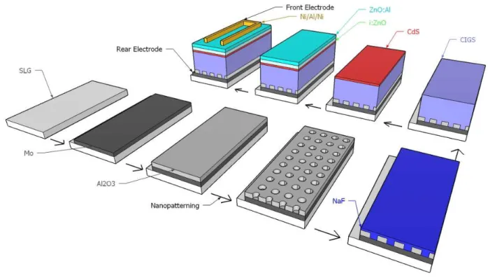
5 Two types of solar cells were prepared: a) a reference solar cell with the standard CIGS solar cell structure; b) a solar cell with an Al2O3 nanopatterned layer in-between the Mo and the CIGS, the so-called passivation layer, as represented in Fig. 1. The Al2O3 layer was nanopatterned using e-beam lithography and a dry etching process to produce openings of ~400 nm with a pitch of 2000 nm. The ultrathin CIGS absorber layer is 350 nm thick, so that the effects of rear interface recombination have a stronger impact on the cell performance. Moreover, the CIGS layer has no elemental gradients. The importance of having flat, ungraded, profiles, is to avoid complementary rear surface passivation effects as those that would be caused by the quasi-electric field of the Ga gradient [49]. We highlight the fact that with the exception of the passivation layer, all the solar cell processing was exactly the same for both solar cells.
Figure 1: representation of the solar cell fabrication process of the passivation sample. The reference device excluded the Al2O3 deposition and the nanopatterning steps.
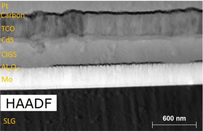
Fig. 2) shows a cross section high angle annular dark-field (HAADF) TEM image of the passivated solar cell. All of the solar cells layers, Mo, Al2O3, CIGS, CdS and the ZnO are visible, together with the TEM preparation layers. We note that a layer consisting of Mo and Sewith a thickness value
6 between 15 to 25 nm is visible in the Mo/CIGS interface exposed by the point contacts. The bright layer on the bottom is the rear contact, Mo, and on top the passivation layer with the nanopatterned openings is visible. The openings, or point contacts, in the 18 nm thick Al2O3 layer have an equivalent area similar to a circle of 400 nm as defined during the exposure and etching. Since the Al2O3 is an insulator, they allow for electrical contact between the rear contact and the CIGS absorbing layer. The TEM image showing the presence of the Al2O3 layer demonstrates that the Al2O3 layer with the nanopatterned contacts are sufficiently robust to withstand the harsh CIGS growth conditions, i.e. 530 oC in a Se atmosphere.
Figure 2: TEM HAADF image of the cross-section of the passivated solar cell. The dark layer in-between the Mo layer and the CIGS layer, is the Al2O3 passivation layer. The observed openings on this Al2O3 layer are the nanopatterned point contacts.
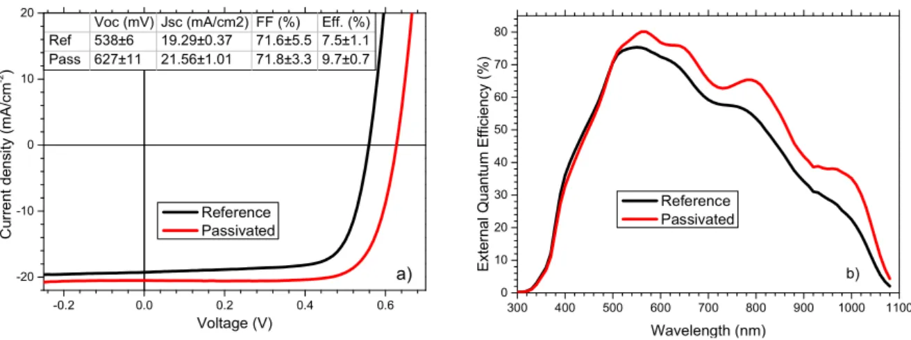
7 Fig. 3a) shows representative J-V curves and Fig. 3b) the corresponding EQE spectra of devices with and without the passivation layer. The inset of Fig. 3a) shows average values together with standard deviations of the figures of merit of the solar cells. The shown curves are representative and were chosen with J-V parameters close to the average values. Both cells show good diode-like behavior without any evidence of blocking behavior. Despite good FF (> 70%) and moderate VOC values (> 500 mV), we note that the efficiency of both cells is being limited mostly by low JSC values (< 21 mA/cm2). We attribute the low J
SC values due to the very thin CIGS layer, 350 nm, which is not sufficient to fully absorb incoming light. Such thin layer leads to high optical losses in the near infrared region. These absorbers are also heavily affected by rear interface recombination, making them ideal to evaluate the effects of the passivation layer. The differences between the two cells are striking, the reference cells achieve, in average, an efficiency value of 7.5% whereas the passivated devices exhibit a value of 9.7%. This large increase in efficiency is due to an increase from 538 mV to 627 mV in VOC, and an increase from 19.29 mA/cm2 to 21.56 mA/cm2 in JSC. The difference in the JSC is seen in the EQE, since the passivated solar cell has a superior performance to the reference one throughout the whole spectrum. In terms of standard deviations, both cells have similar variations in terms of VOC, the passivated solar cell has a higher deviation of results in JSC but a smaller one in FF. This translates into a smaller spread of efficiency values for the passivated solar cell showing more uniform results. The J-V analysis shows that the passivation procedure is beneficial and produces devices with a superior electrical performance in terms of Voc and JSC. It can be pointed out that the passivated devices are quite stable, one year after their fabrication and first measurements, the electrical performance was, within error measurements, the same.
C-V measurements were also performed on all solar cells and the CIGS doping concentration was extracted at the 0 V point [50]. The reference device has a median CIGS (apparent) doping concentration at 0 V of 3.2x1016 cm-3 with a standard deviation of 0.3x1016 cm-3 whereas the passivated devices present an average of 1.9x1016 cm-3 with a standard deviation of 0.3x1016 cm-3. These values
8 are close to error values of the measurement and show that the Na concentration of the two solar cells is similar. -0.2 0.0 0.2 0.4 0.6 -20 -10 0 10 20 C ur re nt d en si ty ( m A /c m -2 ) Voltage (V) Reference Passivated
Voc (mV) Jsc (mA/cm2) FF (%) Eff. (%) Ref 538±6 19.29±0.37 71.6±5.5 7.5±1.1 Pass 627±11 21.56±1.01 71.8±3.3 9.7±0.7 a) 300 400 500 600 700 800 900 1000 1100 0 10 20 30 40 50 60 70 80 E xt er na l Q ua nt u m E ffi ci en cy ( % ) Wavelength (nm) Reference Passivated b)
Figure 3: a) J-V curves of representative cells and the table shows averages with standard variation values of J-V parameters for 12 cells. b) EQE of the same representative devices shown in a).
Optical simulations
In order to further understand the JSC gain of the passivated solar cells, we performed detailed electromagnetic simulations to verify if the attained current gains are due to optical (e.g. from an increased reflection of the rear contact) or electronic effects caused by the passivation layer. The computations were performed with a FDTD mesh-based solver, as discussed further elsewhere [51,52]. The simulated structure was based in the dimensions of the solar cells: ZnO thickness of 440 nm; CdS 70 nm; CIGS 350 nm; MoSe2 25 nm or Al2O3 18 nm; Mo 350 nm [53], in agreement with the TEM image of Fig. 2). The complex refractive index (n,k) values of CIGS with [Ga]/([Ga]+[In]) = 0.31 were taken from [54].
The simulation results are given in Fig. 4a,b), which shows the photo-carrier generation rate profiles and light absorption spectra along the corresponding solar cells stack, for devices with and without (reference) the passivation layer. Only the light absorbed in the GIGS (termed useful absorption) leads to significant photo-current. The parasitic light absorption by the solar cell stack that does not translate into photo-current occurs mainly in: i) the UV range due to the light absorption in
9 the ZnO-based transparent conductive oxide (TCO) and in the CdS layer, where the low minority carrier lifetime does not allow for current output; ii) the near-infrared (NIR) range due to both the free carriers light absorption in the TCO layer [55,56] and the absorption of the Mo rear contact [57,58]. These optical losses account for the difference shown in Fig. 4b) between the light absorption of the CIGS layer and that in the complete solar cell stack.
One of the initial studies performed with the simulations was the investigation of the contribution of the CIGS material inside the point contact in the overall cell absorption, and its possible optical influence in the rest of the CIGS layer. Even though the openings correspond to a very small area, they could create a sub-wavelength effect that is worth exploring. For that, we simulated Al2O3 passivation layers with and without the hole and arrived to the conclusion that, at least optically, the extra CIGS placed inside the Al2O3 layer does not significantly influence the absorption spectra. On the simulation of the structures shown in Fig. 4a) and if we consider a unitary internal quantum efficiency (IQE = 1) in the range of 300 to 1100 nm, i.e. all the light absorbed by the CIGS would generate carriers, we would reach an optical JSC value of 28.50 mA/cm2 for the reference solar cell and 29.40 mA/cm2 for the passivated solar cell. Such computed JSC values are obviously higher than those measured in Fig. 3a) since they only account for optical effects and neglect electrical losses. The higher simulated JSC value attained by simulating the passivated solar cell structure is due to its improved reflection, by interference fringes, occurring at NIR wavelengths (700-1000 nm), see Fig. 4b). Such interference fringes are caused by the improvement of the reflection from the rear Al2O3/Mo surface. Experimentally, the increased interference fringes in the same wavelength region for the passivated solar cell are visible in Fig. 3b), also demonstrating a good fit of the simulation with the experimental results.
10 Figure 4: Optical results for the two solar cell structures without (reference cell) and with the passivation layer (passivated cell). a) Computed carrier generation profiles for both analyzed device structures. b) Simulated light absorption of the full solar cell stacks (dashed lines, total absorption) and of only the CIGS layer (solid lines, useful absorption) for the two device structures with and without the passivation layer. c) Corresponding measured/experimental total absorptance (100% - total reflection).
It should be noted that the difference between the simulated JSC values (0.9 mA/cm2) is significantly lower than that between the measured JSC values (~2.3 mA/cm2) in Fig. 2a). Therefore, such JSC difference observed in the J-V measurements cannot be ascribed merely to optical effects and should be also caused by the electrical passivation behavior of the Al2O3 nanopatterned layer.
11 Photoluminescence
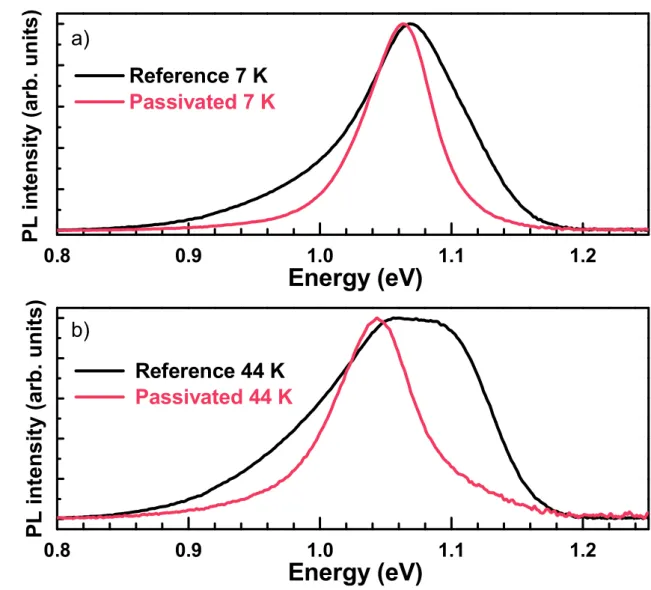
Photoluminescence probes the electronic structure of semiconductors and can be used to arrive to a qualitative evaluation of the effects of passivation layers, in particular to the influence of defects, being those radiative or non-radiative. The normalized PL spectra of the two solar cells, measured at 7 K, under an excitation power of 29 mW and equivalent experimental conditions, are presented in Fig. 5a). Two broad and asymmetric bands with a maximum intensity at 1.07 and 1.06 eV are observed for the reference and passivated solar cells, respectively. Broad emission is typical of Cu-poor CIGS polycrystalline solar cells [42], [43], however, for the case of the reference solar cell, the luminescence is significantly broader than that of the passivated cell. Additionally, the reference solar cell also shows a larger asymmetry in the low energy side of the spectrum suggesting the existence of a higher influence of defects [62,63]. Regarding the passivated solar cell, the full width at half maximum (FWHM) is significantly lower (~61 meV) than that of the reference solar cell (~96 meV). With the increase of temperature (Fig. 5b)), the FWHM value of both solar cells increases, as expected. Still, at higher temperatures, in the case of the passivated solar cells, the shape of the luminescence band is very similar to the one measured at low temperature, although with a slight redshift, while for the reference solar cell there are significant changes that further indicate the presence of the additional radiative transitions. Since the CIGS layer is nominally the same, the changes in PL must be related with the passivation of the rear surface of the absorber layer. In the literature, in addition to the shape of the PL emission at low temperature, to infer the effect of the passivation layer, quite often it is performed a comparison of the PL intensity [64–68]. However, a direct comparison of PL intensity from different samples should be done with caution due to the necessarily different optical alignments despite nominally equivalent experimental conditions and as in this work we do not have those capabilities we do not perform that comparison here. With the used excitation wavelength, 514.5 nm, the incident photons penetration depth, ~70 nm, is smaller than the CIGS thickness, 350 nm. However, the generated charge carriers feel the modification of the density of interface defects induced by the Al2O3 deposition due to the CIGS high carrier diffusion length [69,70] suggesting a
12 different electronic structure in both solar cells caused by the passivation of the rear interface which lowers the interface defects concentration.
0.8
0.9
1.0
1.1
1.2
0.8
0.9
1.0
1.1
1.2
Reference 44 K
Passivated 44 K
P
L
in
te
n
s
it
y
(
ar
b
. u
n
it
s
)
Energy (eV)
b)
(b
)
Reference 7 K
Passivated 7 K
P
L
i
n
te
n
s
it
y
(
a
rb
. u
n
it
s
)
Energy (eV)
a)
Figure 5: Normalized PL spectra of the reference and passivated solar cells under an excitation power of 29 mW and measured at: a) 7 K; b) 44 K.
Discussion
Since both devices have exactly the same layers except the rear Al2O3 passivation layer, we link the differences in the cells performance directly to the effect of the passivation layer. The passivation vastly reduces the total electrical contacting area but, remarkably, the FF values of both cells are still acceptable and very similar, 71.6% for the reference and 71.8% for the passivated one. A good FF value is a sign that the contacting area is well defined and feats the CIGS material properties
13 has low FF values, together with evidences of series resistance, are good indications of point contact structures which are not optimized[71]. For the passivated solar cell, these high values of FF show that the nanopatterned passivation layer in terms of density and spacing design forms an effective contacting area. However, we note that there is a difference of 89 mV between both devices in VOC. With an increase of VOC, FF is expected to follow. Using the well-known equation that relates VOC with FF [72,73]:
𝐹𝐹 =𝜈 − 𝑙𝑛(𝜈 + 0.72) 𝜈 + 1
where 𝜈 is the normalized voltage defined as Voc/(AkT/q), A is the ideality factor of the cell, k the Boltzmann's constant, T the temperature and q the electron charge and considering the ideality values, A, of 0.92 and 1.13 for the reference and the passivated cell, respectively, it is possible to estimate that the passivated device should have a FF value around 3% higher than the passivated solar cell due to its higher VOC value. Hence, more optimization to increase the value of the FF of the passivated devices has to be made by for instance tuning the thickness of the Al2O3 layer and the dimensions of the nanopattern, which could improve the non-ideal rear contact resistance, or by tuning of the alkalis content. With regards to J-V behavior, we note that the reference cell shows some signs of shunting which are not present in the passivated cell. However, a dark J-V measurement of the reference device showed no evidence of shunting. Such fact is a good indication that instead of shunting, the reference cells are being affected by voltage-dependent current collection (VDCC). VDCC occurs in devices with low values of effective diffusion length and with negligible recombination losses in the space-charge-region. In these conditions, a small change in voltage creates a different depletion region contributing thus to different current collection. Low values of effective diffusion length can be caused either by high bulk- or rear interface-recombination. Thus, we attribute the VDCC of the reference device to its high rear interface recombination. As the rear interface recombination is suppressed in the passivated solar cell, it does not suffer from VDCC.
14 VOC and JSC values are higher for the solar cells with the passivation layer, well above uncertainty and the standard deviations values. Concerning the VOC values, the 89 mV difference between both devices can undoubtedly be attributed to effects caused by the introduction of the Al2O3 layer. The increase of VOC values in devices after the introduction of a passivation layer is something expected and very well known in other type of solar cells due to lower interface recombination [74,75]. With respect to the JSC difference, the EQE results (Fig. 2b)) shows that the gains of the passivated cells are from wavelength values above right 500 nm. Such region is the entire optical region of the absorber layer. Having the gains distributed throughout the whole spectra range is a confirmation of the simulation results that the increase of the JSC is not only due to enhanced optical rear reflection, but also due to electronic effects. Three improvements could lead to such an increase of JSC: i) a lowering of the rear contact interface defect density allowing for a lower effective interface recombination velocity; ii) an increased effective minority carrier diffusion length due to an effective electric field at the rear contact induced by negative charges in the passivation layer; iii) an increased optical reflection of the rear contact. Increased optical reflection would be of high interest as it is one of the limitations of ultrathin CIGS solar cells [76–82]. In fact, several approaches have been tested in order to increase the reflection and light scattering properties of the rear contact [24,83–88]. Such properties can contribute to the enhancement of the optical path length of mostly the weakly-absorbed near infra-red (NIR) photons within the CIGS region, thus enabling higher EQE in the NIR range close to the CIGS bandgap (> 700 nm), as seen in the optical results of Fig. 4b,c). However, our results of Fig. 3b) show a photocurrent increase even for wavelengths down to 500 nm, a region where no optical losses are expected. The optical simulations agree with the interpretation that the increase in JSC of the passivated cell cannot be solely attributed to an increased reflection, as commented in the optical analysis section. Therefore it can be concluded that the effect of introducing the point contact layer increases device performance by somewhat increasing the rear reflection but also significantly by the effect of its electronic passivation role, in agreement with our previous studies [20,89] and contrary to other data interpretation from the literature [35].
15 Another scenario that needs to be addressed is the Na diffusion blocking properties of the Al2O3 layer. One would expect the passivated solar cell to have a lower Na concentration than the reference one. To understand this effect, we focus on the apparent doping concentration values extracted by the C-V measurements. Such measurement shows very similar doping concentration which points towards Na concentration values of both solar cells to be also identical. It has been shown that by introducing Na using a NaF precursor layer with a thickness of 15 nm and 22.5 nm would lead to an increase of VOC of 1 mV and an apparent carrier concentration increase around 1x1016 cm-3 [90]. The experimental difference seen in this work between the reference and the passivated devices is 1.3x1016 cm-3, hinting at the fact that the carrier concentration is not changing the VOC values significantly. Even if the previous experimental results cannot be directly linked to the one presented here due to the ultrathin CIGS layers, since the reference device is actually the one with the higher carrier concentration, using the expression:
∆𝑉 =𝐾 𝑇 𝑞 𝑙𝑛
𝑁 𝑁
where KB is the Boltzmann´s constant, T temperature and q the elemental charge, a VOC difference of 13 mV higher for the reference cell compared with the passivated solar cell can be calculated. Thus, both from previous experimental results and the previous calculation, if the passivated solar cell has a lower amount of Na compared with the reference solar cell, it would be expectable to have a lower VOC.Accordingly, even if there are small differences in the Na content of the two solar cells, its influence on the carrier concentration leads to VOC changes that are contrary to the ones seen by the J-V analysis. From both arguments, we conclude that the VOC differences seen here cannot be explained by differences in Na and/or carrier concentration.
With regards to the PL interaction volume, if we give thought only to optical considerations, the PL analysis would only analyze a top surface layer of 70 nm [91]. However, the fact that the PL measurements are affected by modifications to the rear contact show that the CIGS has a minority carrier diffusion length high enough to allow photo-generated carriers at the surface of the CIGS layer
16 to still interact with the rear contact. This result contrasts with previous observations that the PL could contribute with in-depth probing [92]. However, such procedure was applied to kesterite compounds with a low electrical performance, which are known to have a lower minority carrier diffusion length and significant lower electrical performance than the one of CIGS [93]. Interestingly, the fact that PL is sensitive to the entire CIGS volume is in good agreement with the EQE results. The EQE shows that for all the incoming wavelengths there is a superior quantum efficiency for the passivated solar cells. Low wavelength values, or high energy photons, correspond to light absorption in the CIGS close to the surface, but even there the EQE behavior of the passivated cell is superior. This effect is in full agreement with the PL being also sensitive to changes in the rear interface, as expected in the case where the effects are made in a distance smaller to the carriers diffusion length.
The PL analysis has shown qualitatively that the passivation reduces the number of radiative defects that are active in the CIGS. Such reduction of the number of interface defects by the rear passivation was shown by PL in two evidences: i) the larger FWHM value of the reference solar cell, compared with the passivation one, and ii) the appearance of additional radiative transitions as the temperature increases for the reference solar cell. Concerning the FWHM for the PL in both solar cells, the widening of the PL emission has been directly linked in the literature to worse solar cell performances [94]. We observe that the reference cell has a FWHM of ~96 meV and has an efficiency of 7.5%, whereas the passivation solar cell has an FWHM of ~61 meV and with an efficiency of 9.7%. This relation establishes that the passivation strategy lowers the numbers of active interface defects that rule the CIGS optical-properties leading to a higher solar cell performance. Thus, we can say that the Al2O3 nanopatterned point contact layer lowers the interface recombination at the CIGS rear interface. This results, is in very good agreement with our previous observation using electrical measurements of a lower trap density for CIGS/Al2O3 interfaces [95].
Further work should focus on understanding the properties of the Al2O3 passivation layer after it is exposed to the harsh CIGS growth conditions. These growth conditions, a temperature of 525 oC
17 in a Se atmosphere, have been linked to a change in the electronic properties of the AL2O3 layer [95] and in other dielectric materials, it is known that the inclusion of mid-gap defects significantly changes the material properties even by changing it from an electrical insulator to a conductor compound [96,97]. Hence, a full understanding of the electronic properties of the AL2O3 layer after being exposed is needed to further expand the understanding of this system.
Conclusions
Ultrathin CIGS based solar cells with and without passivation layers were fabricated. The passivation consisted of a nanopatterned 18 nm Al2O3 layer with an array of point contacts that allows for electrical contacting between the CIGS and the Mo layer. By comparing the passivated solar cells with the reference devices, we conclude that the Mo-CIGS usual interface is highly recombinative and that only with an effective passivation scheme, ultrathin CIGS devices can achieve high values of electrical performance. Such fact was observed in several ways and by combining optical simulations with experimental devices. Firstly, the difference in electrical performance of both devices shows that by comparing a passivation device with a non-passivated device, the passivation increases both VOC and JSC. Secondly, the conjugation of the EQE results with the optical simulations shows that the passivation layer improves the NIR light reflection from the rear contact. However, they also show that such effect alone is not sufficient to fully justify the total observed increase of the JSC values (2.3 mA/cm2), which is therefore mainly attributed to electric rather than optical effects. Thirdly, PL measurements show that the passivation reduces defects concentration allowing for higher VOC values. Another gain with the passivation layer is reduced VDCC, which again is a confirmation of the very low recombinative rear interface of the passivation device. Thus, the combination of the characterization techniques used in this work allowed us to identify that the nanopatterned Al2O3 layer is both lowering the concentration of defects and increasing the rear optical reflection. Such contribution is important as previous contributions focused in only of the losses and, thus, the next optimizations of the rear interface will have to account for electric and optic considerations.
18 Altogether, the electrical performance of these cells demonstrates that for ultrathin CIGS the introduction of a rear passivation layer based in a nanopatterned point contact Al2O3 layer increases solar cell electrical performance. The introduction of the nanopatterned Al2O3 layer passivates the rear electrical contact allowing for devices with a 350 nm CIGS layer to achieve power conversion efficiency values close to 10%.
Experimental
The solar cells prepared in this work followed the Ångström solar cell baseline, as presented in Fig. 1, and their layer structure was deposited in the same batch [53]. Two sets of solar cells were prepared, one with the regular solar cell structure – designated as reference, and a second one with a passivation layer – designated as passivated solar cell. From each set, 12 solar cells were fabricated. The passivation layer, a 18 nm Al2O3 layer, was deposited by atomic layer deposition (ALD) on Mo. The nanopattern was first defined by e-beam lithography and consisted of a square array of openings/holes of ~400 nm diameter separated by 2000 nm among them. Such array allows for ~93% passivated area leaving ~3% of the area for contacting. Afterwards, the structures were open using a dry etching process [98]. The patterned passivation layer is the only difference between both types of solar cells. For the CIGS evaporation, flat evaporation rates were used to avoid having Cu- and Ga- depth profiles [99]. The CIGS composition is [Cu]/([Ga]+[In]) = 0.70 and [Ga]/([Ga]+[In]) = 0.295 as estimated by XRF with a thickness of 350 nm estimated by stylus profilometry. Prior to the CIGS deposition, a 15 nm NaF layer was deposited which served as the Na source for the CIGS doping [100].
Completed solar cell devices were characterized by J–V measurements with AM1.5 illumination in a home-built system. Fill factor (FF), efficiency, short-circuit current density (JSC), and open circuit voltage (VOC) were calculated from the J–V curves and the corresponding values given in Fig. 2a) are the average of 12 cells with their respective standard deviation. External quantum efficiency (EQE) was determined under ambient light, using chopped monochromatic light that was scanned through the wavelength interval of 360–1200 nm in 2-nm steps, also in a home built system.
19 The photoluminescence (PL) measurements were carried out on a Bruker IFS 66v Fourier Transform Infrared (FTIR) spectrometer, equipped with a Ge diode detector. The excitation source was a 514.5 nm line of an Ar+ ion laser (spot diameter of ∼1 mm), with a laser power measured at the front of the cryostat window. The solar cells were inserted in a helium gas flow cryostat which allowed the change of temperature in the range 7–300 K. The correction of the detectivity of the Ge detector was performed for all spectra. The apparent free carrier density measurements were performed using C-V measurements on an Autolab PGSTAT302N equipped with the FRA32 module. The measurements were performed in dark using a Faraday cage at room temperature. The amplitude of the AC signal was set to be constant and equal to 10 mV rms and the frequency was constant and equal to 10 kHz. The DC component of the excitation signal ranged from -1.0 V to 0.5 V.
Scanning transmission electron microscopy (STEM) images were taken with a FEI Titan Themis 80-300 kV Cs-probe corrected transmission electron microscope (TEM), operating at 200 kV accelerating potential. The lamellae were prepared in a focused ion beam (FIB) FEI Dual-Beam Helios 450S with FIB Mo-grids, using a technique known as "lift-out" [101]. On top of the solar cell, a protective carbon layer followed by a Pt bi-layer were deposited using the electron beam and the Ga beam [102]. Optical modelling description
A numerical 3D mesh-based finite difference time domain (FDTD) method was employed to model the optical response of the fabricated structures, using a specialized commercial solver [103]. The mesh resolution was adapted to the geometry of the structures and illumination conditions after sets of convergence tests, in order to minimize the computational requirements while maintaining high accuracy. The simulations were corroborated by matching the FDTD optical absorption spectra of the flat multilayered cell structures (without the patterned point contacts) with analytical formalisms based on the transfer matrix method.
The periodicity of the square array of rear point contacts allows the FDTD region to be reduced to a square unit cell with side equal to the array pitch. Specific boundary conditions (BCs) were applied
20 in each face of such region. Artificial absorbing perfect-matching layers were applied on the upper and lower boundaries to absorb all outgoing waves. On the side boundaries, periodic BCs were used to model the infinite periodicity of the structures. Here, due to the symmetries of the structure at normal incidence, symmetric and anti-symmetric BCs are employed which allow simulating only one quadrant of the unit cell.
Acknowledgements
P. M. P. Salomé acknowledges the funding of Fundação para Ciência e Tecnologia (FCT) through the project IF/00133/2015. B. Vermang has received funding from the European Research Council (ERC) under the European Union's Horizon 2020 research and innovation programme (grant agreement n° 715027). CAPES (CAPES-INL 04/14), CNPq and FAPEMIG funding agencies are acknowledged for financial support. The European Union's Horizon 2020 research and innovation programme (grant agreement n° 720887) ARCIGS-M project is acknowledged. M. J. Mendes acknowledges funding from FCT through the grant SFRH/BPD/115566/2016. This project was partially supported by FEDER funds, through the COMPETE 2020 Program, and national funds, through the FCT, under the projects POCI-01-0145-FEDER-007688 (Reference UID/CTM/50025) and ALTALUZ (Reference PTDC/CTM-ENE/5125/2014). The authors also acknowledge partial funding from the European Project BET-EU (H2020-TWINN-2015, grant 692373). The NanoFabrication department at INL, namely João Gaspar and Helder Fonseca, are recognized for the help in the development of nanopatterning.
References
[1] M. A. Green, Y. Hishikawa, W. Warta, E. D. Dunlop, D. H. Levi, J. Hohl-Ebinger, A. W. H. Ho-Baillie, Prog. Photovoltaics Res. Appl. 2017, 25, 668.
[2] R. Kamada, T. Yagioka, S. Adachi, A. Handa, K. F. Tai, T. Kato, H. Sugimoto, in 2016 IEEE 43rd Photovolt. Spec. Conf., IEEE, 2016, pp. 1287–1291.
21 [3] P. Reinhard, F. Pianezzi, B. Bissig, A. Chirila, P. Blosch, S. Nishiwaki, S. Buecheler, A. N.
Tiwari, IEEE J. Photovoltaics 2015, 5, 656.
[4] P. Jackson, R. Wuerz, D. Hariskos, E. Lotter, W. Witte, M. Powalla, Phys. status solidi - Rapid Res. Lett. 2016, 10, 583.
[5] J. H. Werner, J. Mattheis, U. Rau, Thin Solid Films 2005, 480–481, 399. [6] M. Gloeckler, J. R. Sites, Thin Solid Films 2005, 480–481, 241.
[7] A. Sacco, F. Bella, S. De La Pierre, M. Castellino, S. Bianco, R. Bongiovanni, C. F. Pirri, ChemPhysChem 2015, 16, 960.
[8] S. Galliano, F. Bella, C. Gerbaldi, M. Falco, G. Viscardi, M. Grätzel, C. Barolo, Energy Technol. 2017, 5, 300.
[9] E. S. Barnard, B. Ursprung, E. Colegrove, H. R. Moutinho, N. J. Borys, B. E. Hardin, C. H. Peters, W. K. Metzger, P. J. Schuck, Adv. Mater. 2017, 29, 1603801.
[10] J. M. Burst, J. N. Duenow, D. S. Albin, E. Colegrove, M. O. Reese, J. A. Aguiar, C.-S. Jiang, M. K. Patel, M. M. Al-Jassim, D. Kuciauskas, S. Swain, T. Ablekim, K. G. Lynn, W. K. Metzger, 2016, 1, 16015.
[11] J. Shi, X. Xu, D. Li, Q. Meng, Small 2015, 11, 2472.
[12] Y. C. Kim, T.-Y. Yang, N. J. Jeon, J. Im, S. Jang, T. J. Shin, H.-W. Shin, S. Kim, E. Lee, S. Kim, J. H. Noh, S. I. Seok, J. Seo, Energy Environ. Sci. 2017.
[13] J.-P. Correa-Baena, W. Tress, K. Domanski, E. H. Anaraki, S.-H. Turren-Cruz, B. Roose, P. P. Boix, M. Gratzel, M. Saliba, A. Abate, A. Hagfeldt, Energy Environ. Sci. 2017, 10, 1207. [14] J. Zhang, A. Hultqvist, T. Zhang, L. Jiang, C. Ruan, L. Yang, Y. Cheng, M. Edoff, E. M. J.
Johansson, ChemSusChem 2017, DOI 10.1002/cssc.201701160.
[15] B. Vermang, V. Fjällström, J. Pettersson, P. Salomé, M. Edoff, Sol. Energy Mater. Sol. Cells 2013, 117, 505.
[16] P. Casper, R. Hünig, G. Gomard, O. Kiowski, C. Reitz, U. Lemmer, M. Powalla, M. Hetterich, Phys. Status Solidi - Rapid Res. Lett. 2016, 10, 376.
[17] B. Vermang, J. T. Wätjen, V. Fjällström, F. Rostvall, M. Edoff, R. Kotipalli, F. Henry, D. Flandre, Prog. Photovoltaics Res. Appl. 2014, 22, 1023.
22 [18] B. Vermang, J. T. Watjen, C. Frisk, V. Fjallstrom, F. Rostvall, M. Edoff, P. Salome, J. Borme,
N. Nicoara, S. Sadewasser, IEEE J. Photovoltaics 2014, 4, 1644.
[19] G. Sozzi, D. Pignoloni, R. Menozzi, F. Pianezzi, P. Reinhard, B. Bissig, S. Buecheler, A. N. Tiwari, 2015 IEEE 42nd Photovolt. Spec. Conf. PVSC 2015 2015, 8.
[20] B. Vermang, V. Fjällström, J. Pettersson, P. Salomé, M. Edoff, Sol. Energy Mater. Sol. Cells 2013, 117, 505.
[21] E. Jarzembowski, B. Fuhrmann, H. Leipner, W. Fränzel, R. Scheer, Thin Solid Films 2016, 2. [22] J. Kim, S. Park, S. Ryu, J. Oh, B. Shin, Prog. Photovoltaics Res. Appl. 2017, 25, 308.
[23] G. Yin, M. W. Knight, M.-C. van Lare, M. M. Solà Garcia, A. Polman, M. Schmid, Adv. Opt. Mater. 2017, 5, 1600637.
[24] G. Yin, M. Song, S. Duan, P. Manley, D. Greiner, C. A. Kaufmann, M. Schmid, ACS Appl. Mater. Interfaces 2016, 8, 31646.
[25] T.-H. Cheng, W. W. Hsu, C. Y. Huang, J.-A. Lu, J. Y. Chen, C. W. Liu, ECS Transactions 33 2011, pp. 191–197.
[26] A. Hultqvist, T. Sone, S. F. Bent, IEEE J. Photovoltaics 2017, 7, 322.
[27] J. Keller, F. Gustavsson, L. Stolt, M. Edoff, T. Törndahl, Sol. Energy Mater. Sol. Cells 2017, 159, 189.
[28] F. Mollica, J. Goffard, M. Jubault, F. Donsanti, S. Collin, A. Cattoni, L. Lombez, N. Naghavi, in 2016 IEEE 43rd Photovolt. Spec. Conf., IEEE, 2016, pp. 2213–2217.
[29] W. Ohm, W. Riedel, U. Aksunger, D. Greiner, C. A. Kaufmann, M. C. Lux-Steiner, S. Gledhill, in 2015 IEEE 42nd Photovolt. Spec. Conf., IEEE, 2015, pp. 1–5.
[30] W.-W. Hsu, J. Y. Chen, T.-H. Cheng, S. C. Lu, W.-S. Ho, Y.-Y. Chen, Y.-J. Chien, C. W. Liu, Appl. Phys. Lett. 2012, 100, 23508.
[31] P. M. P. Salomé, V. Fjällström, P. Szaniawski, J. P. Leitão, A. Hultqvist, P. A. Fernandes, J. P. Teixeira, B. P. Falcão, U. Zimmermann, A. F. da Cunha, M. Edoff, Prog. Photovoltaics Res. Appl. 2015, 23, 470.
[32] M. A. Contreras, K. Ramanathan, J. AbuShama, F. Hasoon, D. L. Young, B. Egaas, R. Noufi, Prog. Photovoltaics Res. Appl. 2005, 13, 209.
23 [33] R. Klenk, Thin Solid Films 2001, 387, 135.
[34] M. Gloeckler, J. R. Sites, Thin Solid Films 2005, 480–481, 241.
[35] E. Jarzembowski, B. Fuhrmann, H. Leipner, W. Fränzel, R. Scheer, Thin Solid Films 2016, 2. [36] P. Reinhard, F. Pianezzi, B. Bissig, A. Chirila, P. Blosch, S. Nishiwaki, S. Buecheler, A. N.
Tiwari, IEEE J. Photovoltaics 2015, 5, 656.
[37] B. Vermang, J. T. Watjen, C. Frisk, V. Fjallstrom, F. Rostvall, M. Edoff, P. Salome, J. Borme, N. Nicoara, S. Sadewasser, IEEE J. Photovoltaics 2014, 4, 1644.
[38] G. Sozzi, S. Di, R. Menozzi, B. Bissig, S. Buecheler, A. N. Tiwari, Sol. Energy Mater. Sol. Cells 2017, 165, 94.
[39] A. Bercegol, B. Chacko, R. Klenk, I. Lauermann, M. C. Lux-Steiner, M. Liero, J. Appl. Phys. 2016, 119, DOI 10.1063/1.4947267.
[40] M. Nerat, Sol. Energy Mater. Sol. Cells 2012, 104, 152.
[41] T. Umehara, S. Iinuma, A. Yamada, Electron. Mater. Lett. 2016, 12, 479.
[42] Z. J. Li-Kao, N. Naghavi, F. Erfurth, J. F. Guillemoles, I. Gérard, A. Etcheberry, J. L.
Pelouard, S. Collin, G. Voorwinden, D. Lincot, Prog. Photovoltaics Res. Appl. 2012, 20, 582. [43] J. Posada, M. Jubault, N. Naghavi, Thin Solid Films 2017, 633, 66.
[44] N. Naghavi, F. Mollica, J. Goffard, J. Posada, A. Duchatelet, M. Jubault, F. Donsanti, A. Cattoni, S. Collin, P. P. Grand, J. J. Greffet, D. Lincot, Thin Solid Films 2017, 633, 55. [45] E. Jarzembowski, B. Fuhrmann, H. Leipner, W. Fränzel, R. Scheer, Thin Solid Films 2017,
633, 61.
[46] O. Lundberg, M. Bodegård, J. Malmström, L. Stolt, Prog. Photovoltaics Res. Appl. 2003, 11, 77.
[47] F. Mollica, M. Jubault, F. Donsanti, A. Loubat, M. Bouttemy, A. Etcheberry, N. Naghavi, Thin Solid Films 2017, 633, 202.
[48] M. Edoff, S. Schleussner, E. Wallin, O. Lundberg, Thin Solid Films 2011, 519, 7530. [49] O. Lundberg, M. Edoff, L. Stolt, Thin Solid Films 2005, 480–481, 520.
[50] P. M. P. Salomé, V. Fjallstrom, A. Hultqvist, P. Szaniawski, U. Zimmermann, M. Edoff, Prog. Photovoltaics Res. Appl. 2014, 22, 83.
24 [51] M. J. Mendes, A. Araújo, A. Vicente, H. Águas, I. Ferreira, E. Fortunato, R. Martins, Nano
Energy 2016, 26, 286.
[52] A. T. Vicente, P. J. Wojcik, M. J. Mendes, H. Águas, E. Fortunato, R. Martins, Sol. Energy 2017, 144, 232.
[53] J. Lindahl, U. Zimmermann, P. Szaniawski, T. Torndahl, A. Hultqvist, P. Salomé, C. Platzer-Björkman, M. Edoff, IEEE J. Photovoltaics 2013, 3, 1100.
[54] P. D. Paulson, R. W. Birkmire, W. N. Shafarman, J. Appl. Phys. 2003, 94, 879.
[55] A. Lyubchyk, A. Vicente, P. U. Alves, B. Catela, B. Soule, T. Mateus, M. J. Mendes, H. Águas, E. Fortunato, R. Martins, Phys. status solidi 2016, 213, 2317.
[56] A. Lyubchyk, A. Vicente, B. Soule, P. U. Alves, T. Mateus, M. J. Mendes, H. Águas, E. Fortunato, R. Martins, Adv. Electron. Mater. 2016, 2, DOI 10.1002/aelm.201500287. [57] K. Orgassa, H. W. Schock, J. H. Werner, Thin Solid Films 2003, 431–432, 387. [58] Z. J. Li-Kao, N. Naghavi, F. Erfurth, J. F. Guillemoles, I. Gérard, A. Etcheberry, J. L.
Pelouard, S. Collin, G. Voorwinden, D. Lincot, Prog. Photovoltaics Res. Appl. 2012, 20, 582. [59] H. Limborço, P. M. P. Salomé, J. P. Teixeira, D. G. Stroppa, R.-R. Andrade, N. Nicoara, K.
Abderrafi, J. P. Leitão, J. C. Gonzalez, S. Sadewasser, CrystEngComm 2016, 18, 7147.
[60] I. Dirnstorfer, M. Wagner, D. M. Hofmann, M. D. Lampert, F. Karg, B. K. Meyer, Phys. status solidi 1998, 168, 163.
[61] P. M. P. Salomé, V. Fjällström, P. Szaniawski, J. P. Leitão, A. Hultqvist, P. A. Fernandes, J. P. Teixeira, B. P. Falcão, U. Zimmermann, A. F. da Cunha, M. Edoff, Prog. Photovoltaics Res. Appl. 2015, 23, 470.
[62] J. P. Teixeira, R. A. Sousa, M. G. Sousa, A. F. da Cunha, P. A. Fernandes, P. M. P. Salomé, J. P. Leitão, Phys. Rev. B 2014, 90, 235202.
[63] J. P. Teixeira, R. A. Sousa, M. G. Sousa, A. F. da Cunha, P. A. Fernandes, P. M. P. Salomé, J. C. González, J. P. Leitão, Appl. Phys. Lett. 2014, 105, 163901.
[64] J. Joel, B. Vermang, J. Larsen, O. Donzel-Gargand, M. Edoff, Phys. Status Solidi - Rapid Res. Lett. 2015, 9, 288.
25 Tsai, C.-W. Liu, H. A. Atwater, W. A. Goddard, J.-H. Lee, J. R. Greer, Acta Mater. 2016, 106, 171.
[66] Y. S. Lee, T. Gershon, T. K. Todorov, W. Wang, M. T. Winkler, M. Hopstaken, O. Gunawan, J. Kim, Adv. Energy Mater. 2016, 6, 1.
[67] W.-W. Hsu, J. Y. Chen, T.-H. Cheng, S. C. Lu, W.-S. Ho, Y.-Y. Chen, Y.-J. Chien, C. W. Liu, Appl. Phys. Lett. 2012, 100, 23508.
[68] J. Kim, S. Park, S. Ryu, J. Oh, B. Shin, Prog. Photovoltaics Res. Appl. 2017, 25, 308.
[69] T. Dullweber, O. Lundberg, J. Malmström, M. Bodegård, L. Stolt, U. Rau, H. W. Schock, J. H. Werner, Thin Solid Films 2001, 387, 11.
[70] G. Brown, V. Faifer, A. Pudov, S. Anikeev, E. Bykov, M. Contreras, J. Wu, Appl. Phys. Lett. 2010, 96, 22104.
[71] G. Sozzi, S. Di, R. Menozzi, B. Bissig, S. Buecheler, A. N. Tiwari, Sol. Energy Mater. Sol. Cells 2017, 165, 94.
[72] M. A. Green, Solar Cells: Operating Principles, Technology, and System Applications, Englewood Cliffs, NJ, USA: Prentice-Hall, 1982.
[73] P. M. P. Salome, A. Hultqvist, V. Fjallstrom, M. Edoff, B. G. Aitken, K. Zhang, K. Fuller, C. Kosik Williams, IEEE J. Photovoltaics 2014, 4, 1659.
[74] S. W. Glunz, D. Biro, S. Rein, W. Warta, J. Appl. Phys. 1999, 86, 683.
[75] M. Taguchi, A. Terakawa, E. Maruyama, M. Tanaka, Prog. Photovoltaics Res. Appl. 2005, 13, 481.
[76] C. van Lare, G. Yin, A. Polman, M. Schmid, ACS Nano 2015, 9, 9603. [77] G. Yin, P. Manley, M. Schmid, Sol. Energy Mater. Sol. Cells 2016, 153, 124.
[78] G. Yin, M. Song, S. Duan, P. Manley, D. Greiner, C. A. Kaufmann, M. Schmid, ACS Appl. Mater. Interfaces 2016, 8, 31646.
[79] M. Schmid, Semicond. Sci. Technol. 2017, 32, 43003.
[80] N. Barange, V. Ben Chu, M. Nam, I.-H. Ahn, Y. D. Kim, I. K. Han, B. K. Min, D.-H. Ko, Adv. Energy Mater. 2016, 6, 1601114.
26 Adv. 2016, 6, 60643.
[82] Y.-C. Wang, H.-Y. Cheng, Y.-T. Yen, T.-T. Wu, C.-H. Hsu, H.-W. Tsai, C.-H. Shen, J.-M. Shieh, Y.-L. Chueh, ACS Nano 2015, 9, 3907.
[83] S. Schleussner, T. Kubart, T. Törndahl, M. Edoff, Thin Solid Films 2009, 517, 5548. [84] B. Vermang, J. T. Wätjen, V. Fjällström, F. Rostvall, M. Edoff, R. Gunnarsson, I. Pilch, U.
Helmersson, R. Kotipalli, F. Henry, D. Flandre, Thin Solid Films 2015, 582, 300. [85] C. van Lare, G. Yin, A. Polman, M. Schmid, ACS Nano 2015, 9, 9603.
[86] G. Yin, P. Manley, M. Schmid, Sol. Energy Mater. Sol. Cells 2016, 153, 124. [87] M. Schmid, Semicond. Sci. Technol. 2017, 32, 43003.
[88] K. Orgassa, H. W. Schock, J. H. Werner, Thin Solid Films 2003, 431–432, 387. [89] C. Frisk, C. Platzer-Björkman, J. Olsson, P. Szaniawski, J. T. Wätjen, V. Fjällström, P.
Salomé, M. Edoff, J. Phys. D. Appl. Phys. 2014, 47, 485104.
[90] P. M. P. Salomé, A. Hultqvist, V. Fjällström, M. Edoff, B. Aitken, K. Vaidyanathan, K. Zhang, K. Fuller, C. Kosik Williams, IEEE J. Photovoltaics 2013, 3, 852.
[91] P. M. P. Salome, J. P. Teixeira, J. Keller, T. Torndahl, S. Sadewasser, J. P. Leitao, IEEE J. Photovoltaics 2017, 7, 670.
[92] P. M. P. Salomé, P. A. Fernandes, J. P. Leitão, M. G. Sousa, J. P. Teixeira, A. F. da Cunha, J. Mater. Sci. 2014, 49, 7425.
[93] T. Gokmen, O. Gunawan, T. K. Todorov, D. B. Mitzi, Appl. Phys. Lett. 2013, 103, DOI 10.1063/1.4820250.
[94] T. Gokmen, O. Gunawan, T. K. Todorov, D. B. Mitzi, Appl. Phys. Lett. 2013, 103, DOI 10.1063/1.4820250.
[95] R. Kotipalli, B. Vermang, J. Joel, R. Rajkumar, M. Edoff, D. Flandre, AIP Adv. 2015, 5. [96] Z. Q. Liu, D. P. Leusink, W. M. Lü, X. Wang, X. P. Yang, K. Gopinadhan, Y. T. Lin, A.
Annadi, Y. L. Zhao, A. R. Barman, S. Dhar, Y. P. Feng, H. B. Su, G. Xiong, T. Venkatesan, Ariando, Phys. Rev. B 2011, 84, 165106.
[97] Z. Q. Liu, W. Lu, S. W. Zeng, J. W. Deng, Z. Huang, C. J. Li, M. Motapothula, W. M. Lü, L. Sun, K. Han, J. Q. Zhong, P. Yang, N. N. Bao, W. Chen, J. S. Chen, Y. P. Feng, J. M. D.
27 Coey, T. Venkatesan, Ariando, Adv. Mater. Interfaces 2014, 1, DOI 10.1002/admi.201400155. [98] B. Vermang, J. T. Watjen, C. Frisk, V. Fjallstrom, F. Rostvall, M. Edoff, P. Salome, J. Borme,
N. Nicoara, S. Sadewasser, IEEE J. Photovoltaics 2014, 4, 1644.
[99] P. M. P. Salomé, A. Hultqvist, V. Fjällström, B. Vermang, M. Edoff, B. Aitken, K. Zhang, K. Fuller, C. Kosik Williams, Sol. Energy Mater. Sol. Cells 2014, 123, 166.
[100] P. M. P. Salome, A. Hultqvist, V. Fjallstrom, M. Edoff, B. G. Aitken, K. Zhang, K. Fuller, C. Kosik Williams, IEEE J. Photovoltaics 2014, 4, 1659.
[101] S. Bals, W. Tirry, R. Geurts, Z. Yang, D. Schryvers, Microsc. Microanal. 2007, 13, 80. [102] P. M. P. Salome, R. Ribeiro-Andrade, J. P. Teixeira, J. Keller, T. Torndahl, N. Nicoara, M.
Edoff, J. C. Gonzalez, J. P. Leitao, S. Sadewasser, IEEE J. Photovoltaics 2017, 7, 858. [103] “Lumerical Solutions, Inc.,” can be found under
28 List of Figures:
Figure 1: representation of the solar cell fabrication process of the passivation sample. The reference device excluded the Al2O3 deposition and the nanopatterning steps.
Figure 2: TEM HAADF image of the cross-section of the passivated solar cell. The dark layer in-between the Mo layer and the CIGS layer, is the Al2O3 passivation layer. The observed openings on this Al2O3 layer are the nanopatterned point contacts.
Figure 3: a) J-V curves of representative cells and the table shows averages with standard variation values of J-V parameters for 12 cells. b) EQE of the same representative devices shown in a).
Figure 4: Optical results for the two solar cell structures without (reference cell) and with the passivation layer (passivated cell). a) Computed carrier generation profiles for both analysed device structures. b) Simulated light absorption of the full solar cell stacks (dashed lines, total absorption) and of only the CIGS layer (solid lines, useful absorption) for the two device structures with and without the passivation layer. c) Corresponding measured/experimental total absorptance (100% - Total Reflection).
Figure 5: Normalised PL spectra of the reference and passivated solar cells under an excitation power of 29 mW and measured at: a) 7 K; b) 44 K.