Ano 2009/2010
João Pedro Mire
Dores Pulido
Valente
Filmes de Óxido de Cálcio, Cobre e
Titânio para Aplicações
Microelectrónicas
Calcium Copper Titanium Oxide Thin Films for
Microelectronic Applications
Universidade de Aveiro
Ano 2009/2010
Departamento de Engenharia Cerâmica e do Vidro
João Pedro Mire
Dores Pulido
Valente
Filmes de Óxido de Cálcio, Cobre e
Titânio para Aplicações
Microelectrónicas
Calcium Copper Titanium Oxide Thin Films for
Microelectronic Applications
A thesis submitted in partial fullfilment of the requirements of the European Master in Material Science (EMMS) degree presented to Universidade de Aveiro under the supervision of Dr. Aiying Wu, Senior researcher from CICECO, Centre for Research in Ceramics and Composite Materials, University of Aveiro, and co-supervision of Prof. Paula Maria Vilarinho, Associate Professor of the University of Aveiro.
Financial support from FCT within the project “Perovskite thin films with colossal dielectric constant prepared by chemical solution deposition for microelectronic and sensor applications”, PTDC/CTM/73367/2006. Financial support from European Commission in the aim of European Masters in Material Science.
The jury
president Doutor Pedro Quintanilha Mantas
Professor Auxiliar da Universidade de Aveiro
Doutor José Ramiro Afonso Fernandes
Professor Auxiliar da Universidade Trás-os- Montes e Alto Douro
Doutora Paula Maria Lousada Silveirinha Vilarinho
Professora Associada da Universidade de Aveiro
Doutora Aiying Wu
1. Acknowledgements
Authors’ first acknowledgements go to a very important person in this work, my supervisor, since she is the project leader and a brilliant researcher, Drª. Aiying Wu. I would like also to thank her for giving me the opportunity to work in this project and give her my best wishes.
I want to take this opportunity to thank also to my co-advisors, Professor Paula Vilarinho and Professor Gerold Schneider, for scientific contribution and guidance in the work.
Special thanks to MSc. Rodrigo Pacher at Technical University of Harburg - Hamburg for the knowledge he was able to transmit me with the AFM technique.
I would also like to thank to Eng. Maria da Conceição Costa for the XRD measurements, Dr. Marta Ferro and Eng. Ana Margarida Silva for the training and help with SEM technique, MSc. Célia Miranda and Eng. Ana Ribeiro for the solutions characterization. Their kindness, patience and sympathy will always be remembered.
A general acknowledgment to the groups that, so well, hosted me during this journey, Electroceramics Group of CICECO at the University of Aveiro and Advanced Ceramics Group at the Technical University of Harburg Hamburg.
I would like to thank specially to my parents, sister and family for all the support, understanding and love given to me.
For their friendship, share and laughs I want to thank, André, Filipe, João, Maria João, Pedro and Rui.
I want to acknowledge all the others that share tiny moments but very important, in Aveiro and Hamburg, during the time spent developing this work.
2. Abstract
Recent research has shown that the perovskite-related body-centred cubic material CaCu3Ti4O12
(CCTO) exhibit extraordinarily giant dielectric constant at room temperature (ε ≈ 104-105). Besides, these high dielectric constants were found to be nearly constant in the temperature range between 100 and 500K [1, 2]; which makes it even more attractive from the technological point of view. These properties are very important for device implementation and make CCTO a promising candidate for microelectronic applications (like decoupling capacitors, random access memories), microwave devices (for applications in mobile phones), antennas (for example, planar micro-strip antenna on CCTO substrate for 3-GHz operation) [3]. In the microelectronics device field, homogeneous and smooth thin films with colossal dielectric constant and with low dielectric loss are desirable.
In the literature, only five reports on undoped CCTO films on silicon based substrates prepared by sol-gel method can be found. The majority of these authors did not present the dielectric and microstructural properties of the produced CCTO films.
In this work, thin films of CCTO were prepared by sol-gel method by spin coating a nontoxic chemical solution on typical microelectronic substrates, Si (wafer) / SiO2 (300 nm) / TiO2 (20 nm) /
Pt (150 nm). Two different precursor solutions were studied and optimized for film production. These two solutions differ mainly on the titanium precursor, although some preparation parameters where changed as well. One of the main objectives of the thesis was to develop nontoxic precursors for CSD method and accordingly, solutions were prepared without methoxyethanol (highly toxic). This constitutes a great improvement considering the good properties obtained for the 300-400 nm thick CCTO films prepared in this work: dielectric permittivity, ε of 500 and dielectric loss, tan of 0.19, for films derived from titanium butoxide precursor solutions (BUT-CCTO) and ε ≈ 620 and dielectric loss 0.18 for those derived from titanium isopropoxide precursor solutions (ISO-CCTO), all values at 1 kHz.
In literature, toxic precursor solution of CCTO leads to films with values for dielectric permittivity of 1000-2000 and dielectric loss between 0.5 – 0.04 [52]. Best reports on nontoxic solutions for spin coating method presented dielectric constant (≈ 150-250) and losses around 0.2-0.5 [45]. The physical properties of the films were characterised. The structural and microstructural characterization was conducted via X-Ray Diffraction (XRD), Scanning Electron Microscopy (SEM) and Atomic Force Microscopy (AFM).
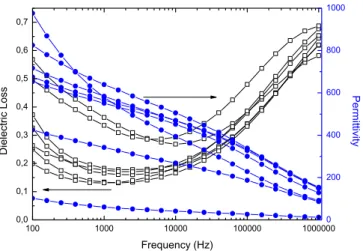
For the electrical characterization the dielectric constant and dielectric losses were measured at room temperature in the range 100 Hz-1 MHz.
AFM microstructure and especially potential images, confirmed IBLC model for conduction, since grain and grain boundaries presented different potentials due to their different electrical behaviour. This result was obtained for every sample made with both solutions.
Grain size has a considerable influence on the dielectric properties of the thin films. grain films present high dielectric constant and high dielectric loss. Small grain origins lower dielectric constant but also low dielectric loss.
In this work and based on IBLC model, it was found that grain and high grain boundaries density will guarantee good permittivity according with [6, 9], although with grain size increase, grain boundaries density decrease. An intermediate stage for grain size must be achieved depending on the solution used. Considering the dielectric loss, it was found to respect mainly to grain boundaries. High density of grain boundaries promotes second phase segregation (TiO2) due to
low temperature heat treatments and worst insulator behaviour [18,24]. For one side, high density will lower dielectric loss confirming [6,13], on the other side, second phase segregation will increase it, as reported in [18, 24].
A compromise between the capacity of the semiconductor grains to admit charges and the resistivity of the insulator grain boundaries must be achieved to obtain good quality CCTO thin films. The admission of charges by the grain is controlled by the grain size (heat treatment procedure) meanwhile the current density of the grain boundaries is controlled by second phase segregation (solution procedure) and grain boundaries density (heat treatment procedure). As a final output of this work a new non-toxic precursor solution was developed as an alternative way for preparing CCTO thin films of high dielectric constant for microelectronic applications.
Keywords:Calcium Copper Titanium Oxide (CCTO), Thin Films, Spin Coating, Nontoxic Precursor, Colossal Permittivity, Microelectronic.
List of Contents
1. Acknowledgements ... 7
2. Abstract ... 9
3. Thesis Organization ... 15
4. Objectives ... 17
5. State of the art ... 19
5.1 Calcium Copper Titanium Oxide (CCTO) ... 19
5.2 CCTO Thin Films – Preparation Methods and Properties ... 28
6. Experimental ... 37
6.1 Precursor Preparation ... 37
6.2 Thin Film Fabrication ... 40
6.3 Precursor Solution Characterization Techniques ... 42
6.3.1.TG / DTA... 42
6.3.2.Viscosity Measurements... 43
6.4 Thin Film Characterization Techniques ... 43
6.4.1.XRD... 43
6.4.2.SEM ... 44
6.4.3.AFM ... 44
6.4.3.1. Contact Mode ... 45
6.4.3.2. Tapping mode ... 46
6.4.3.3. Kelvin Force Microscopy (Potential Imaging) ... 47
7. Results and Discussion ... 49
7.1 Precursors Solutions Characterization ... 49
7.2 Thin Film Characterization ... 51
7.2.1. ISO-CCTO derived thin films ... 51
7.2.1.1. Structural Characterization... 51
7.2.1.2. Effect of drying step duration ... 53
7.2.1.3. Effect of final annealing temperature... 60
7.2.1.4. Summary ... 66
7.2.2.BUT-CCTO derived thin films... 67
7.2.2.2. Effect of final annealing temperature... 68
7.2.2.3. Summary ... 78
8. Conclusions ... 81
9. References ... 84
10.Appendix A – Thickness study... 87
List of Figures Figure 1 – Dependence of the dielectric constant and dielectric loss with temperature, for different frequencies for CCTO ceramics. One can observe the typical behaviour of CCTO material. [6] ...19
Figure 2 – Structure of the cubic pseudo-perovskite (Im3) CaCu3Ti4O12 with TiO6 octahedra, Cu in square planar coordination (dark blue spheres), O ions at the centre of each face and edge (light blue spheres) and Ca at the origin and cube centre (red spheres).[7] ...20
Figure 3 - Dielectric capacitance (a) and tang δ (b) versus frequency at 300 º K for CCTO ceramics sintered at 1100º C for two different grain sizes, different annealing time [9]. ...21
Figure 4 - Dielectric constant (a) and tang δ (b) versus SnO2 concentration for MW treated and untreated CCTO ceramic samples. [19]...25
Figure 5 - Thickness of CCTO films vs. the coating cycle for SFA, single-cycle furnace annealed at 800 °C and MFA, multi-cycle furnace annealed at 800 °C. On the right, dielectric constants and dissipation factor for single-cycle and multicycle furnace annealed CCTO films as a function of film thickness. ...30
Figure 6 – Solvents studied for the dissolution of calcium and copper acetates. ...37
Figure 7 - Diagram of titanium isopropoxide precursor solution developed using non-toxic solvents...38
Figure 8 - Diagram of titanium butoxide precursor solution, developed using non-toxic solvents. ...39
Figure 9 – DTA (right axis) and TG (left axis) results for titanium isopropoxide solution (ISO -CCTO), main DTA reaction peaks marked with *. ...49
Figure 10 – DTA (right axis) and TG (left axis) res ults for titanium butoxide solution (BUT-CCTO), main DTA reaction peaks marked with *. ...50
Figure 11 – Viscosity data obtained for both solutions produced during this study. ...50
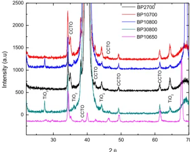
Figure 12 – XRD spectra of ISO-CCTO derived thin films, XRD peaks of CCTO and TiO2 were identified. ...52
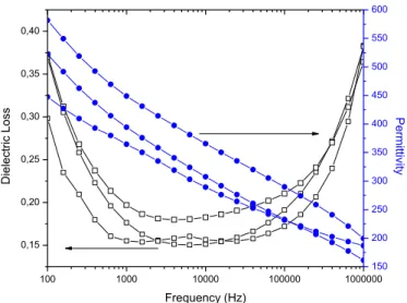
Figure 13 – Dielectric permittivity and diel ectric loss versus frequency for IP2800, thin films dried during 2 minutes and annealed at 800º C. ...53
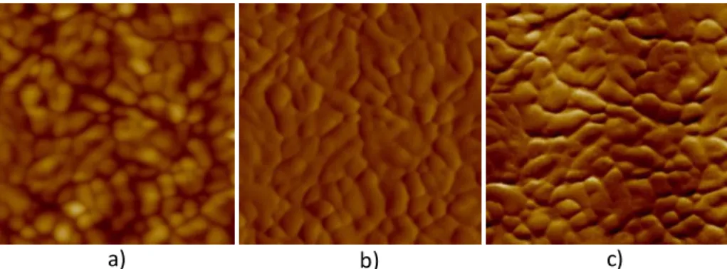
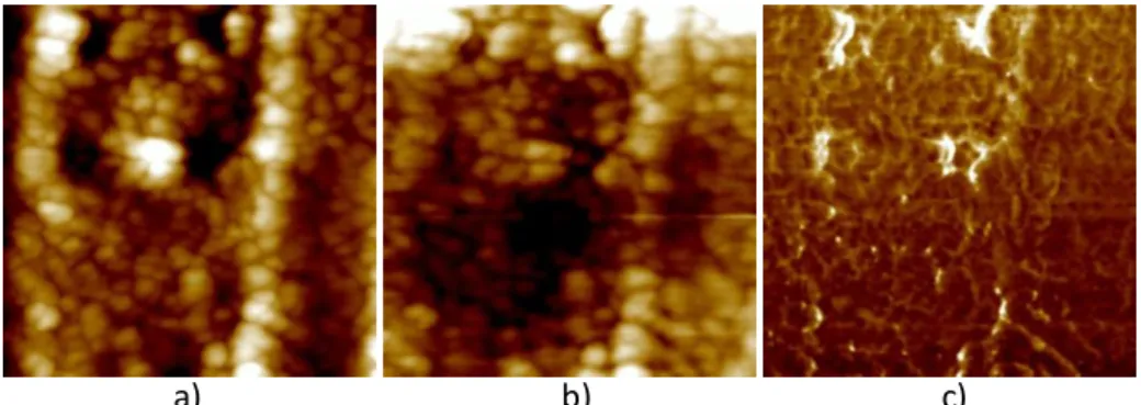
Figure 14 – AFM images in contact mode for IP2800 thin films, a) height (50 nm), b) deflection (50 mU) and c) friction (100 mV), scanned area of 1 µm2...54
Figure 15 – AFM images in tapping mode for IP2800 thin films, a) height (50 nm), b) potential (40 mV) and c) phase (15°), scanned area of 2 µm2. ...54
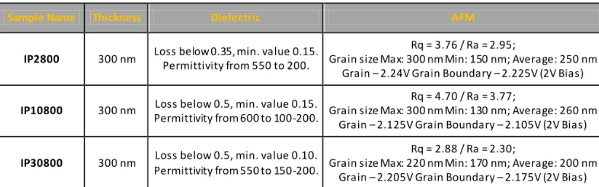
Figure 16 – Dielectric permittivity and dielectric loss versus frequency for IP10800, thin films dried during 10 minutes and annealed at 800º C. ...55
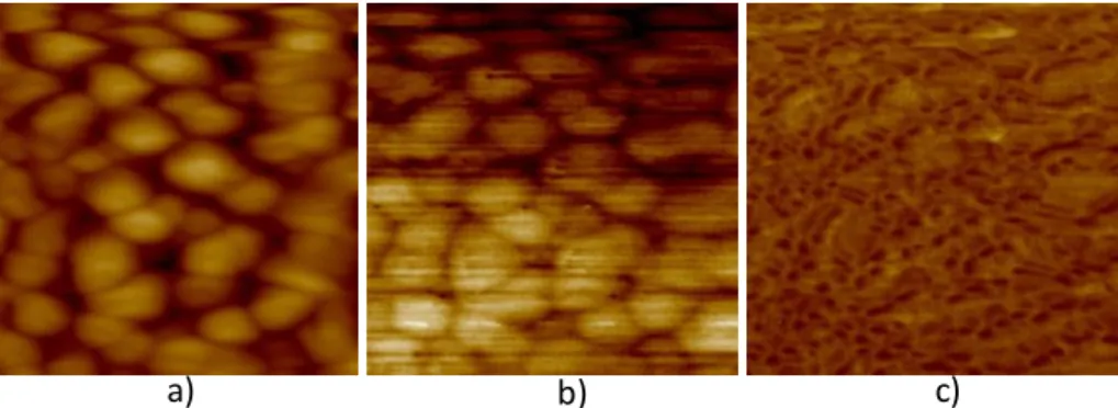
Figure 17 – AFM images in contact mode for IP10800 thin films, a) height (50 nm), b) deflection (50 mU) and c) friction (100 mV), scanned area of 1 µm2...56
Figure 18 – AFM images in tapping mode for IP10800 thin films, a) height (50 nm), b) potential (40 mV) and c) phase (15°), scanned area of 1 µm2...56
Figure 19 – Dielectric permittivity and diel ectric loss versus frequency for IP30800, thin film dried during 30 minutes and annealed at 800º C. ...58
Figure 20 – AFM images in contact mode for IP30800 thin films, a) height (50nm), b) and deflection (50 mU), scanned area of 1 µm2. ...58 Figure 21 – AFM images in tapping mode for IP30800 thin films, a) height (50 nm), b) potential (40 mV) and c) phase (15°), scanned area of 1 µm2...59 Figure 22 – Dielectric permittivity and dielectric loss versus frequency for IP10700, thin films dried during 10 minutes and annealed at 700º C. ...61 Figure 23 – SEM microstructures for IP700 films dried during 10 minutes and annealed at 700 º C, a) cross-section and b) and c) top surface micrograph. ...61 Figure 24 – AFM images for IP10700 thin films in contact mode, a) height (15 nm), b) deflection (35 mU) and c) friction (300 mV), scanned area of 4 µm2...62 Figure 25 – AFM images for IP10700 thin films in tapping mode, a) height (40 nm), b) potential (30 mV) and c) phase (25°), scanned area of 1 µm2...63 Figure 26 – Dielectric permittivity and loss versus frequency plot for IP10750, thin films dried durin g 10 minutes and annealed at 750º C. ...63 Figure 27 – AFM images for IP10750 thin films in contact mode, a) height (15 nm), b) deflection (35 mU) and c) friction (300 mV), scanned area of 4 µm2...64 Figure 28 – AFM images for IP10750 thin films in tapping mode, a) height (40 nm), b) potential (30 mV) and c) phase (25°), scanned area of 1 µm2...64 Figure 29 – Variation of the dielectric permittivity (left axis) and dielectric loss (right axis) function of the grain size for all ISO-CCTO derived thin films...66 Figure 30 - XRD spectra of BUT-CCTO derived thin films, XRD peaks of CCTO and TiO2 were identified...67
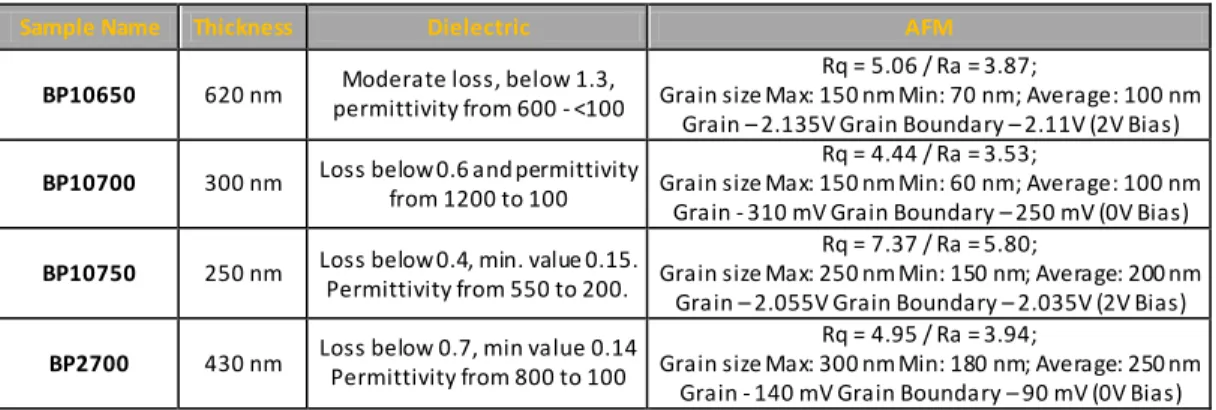
Figure 31 – Dielectric permittivity and dielectric loss versus frequency for BP10650, thin films dried during 10 minutes and annealed at 650º C...69 Figure 32 - SEM microstructures for BP10650 films dried during 10 minutes and annealed at 650 º C, a) and b) top surface micrographs. ...69 Figure 33 – AFM images in contact mode for BP10650 thin films, a) height (50 nm), b) deflection (50 mU) and c) friction (200 mV), scanned area of 2.89 µm2. ...70 Figure 34 – AFM images in tapping mode for BP10650 thin films, a) height (50 nm), b) potential (50 mV) and c) phase (20°), scanned area of 2.89 µm2. ...70 Figure 35 – Dielectric permittivity and dielectric loss versus frequency for BP10700, thin films dried during 10 minutes and annealed at 700º C...71 Figure 36 - SEM microstructures for BP10700 films dried during 10 minutes and annealed at 700º C, a) and b) top surface micrographs, c) cross section view. ...72 Figure 37 – AFM images in contact mode for BP10700 thin films, a) height (40 nm), b) deflection (20 mU) and c) friction (500 mV), scanned area of 4 µm2...72 Figure 38 - AFM images in tapping mode for BP10700 thin films, a) height (75 nm),b) potential (75 mV) and c) phase (30°), scanned area of 4 µm2...73 Figure 39 – Dielectric permittivity and dielectric loss versus frequency for BP10750, thin films dried during 10 minutes and annealed at 750º C...74 Figure 40 – AFM images in contact mode for BP10750 thin films, a) height (40 nm), b) deflection (20 mU) and c) friction (500 mV), scanned area of 4 µm2...74 Figure 41 - AFM images in tapping mode for BP10750 thin films, a) height (75 nm), b) potential (75 mV) and c) phase (30º), scanned area of 4 µm2...75 Figure 42 – Dielectric permittivity and dielectric loss versus frequency for BP2700, thin film dried during 2 minutes and annealed at 700º C. ...76 Figure 43 - SEM microstructures for BP2700 films dried during 2 minutes and annealed at 700 º C sample, a) cross-section and b) and c) top surface micrographs...76
Figure 44 – AFM images in contact mode for BP2700 thin films, a) height (40 nm), b) deflection (30 mU) and c) friction (150 mV), scanned area of 4 µm2...77 Figure 45 – AFM images in tapping mode for BP2700, a) height (50 nm), b) potential (150 mV) and c) phase (30°), scanned area of 4 µm2...77 Figure 46 – Variation of the dielectric permittivity (left axis) and dielectric loss (right axis) function of the thickness for all BUT-CCTO derived thin films, except BP10650. ...79 Figure 47 – Variation of the dielectric permittivity (left axis) and dielectric loss (right axis) function of the grain size for all BUT-CCTO derived thin films, except BP10650 ...79 Figure 48 – Variation of the dielectric permittivity (left axis) and dielectric loss (right axis) function of the ratio between thickness and grain size for all BUT-CCTO derived thin films, except BP10650 ...80
List of Tables
Table 1 – Production parameters for the set of CCTO thin films prepared using ISO nontoxic solution. ...40 Table 2 – Production parameters for the set of CCTO thin films prepared using BUT nontoxic solution...41 Table 3 – Characterization summary for the thin films produced under the study of the effect of drying step duration, 2, 10 and 30 minutes. Thickness is an estimated value from study presented in Appendix A. Rq is the quantitative roughness and Ra the average (RMS) roughness...60 Table 4 – Characterization summary for the thin films produced under the study of the final annealing temperature effect 700, 750 and 800º C. Thickness is an estimated value from study presented in Appendix A, expect for IP10700 that it is the value measured. Rq is the quantitati ve roughness and Ra the average (RMS) roughness. ...65 Table 5 – Characterization summary for the BUT-CCTO derived thin films produced at different final
annealing temperatures 650, 700, 750 and 800º C. In this case, thickness is the real value measured for all films except for BP10750. Rq is the quantitative roughness and Ra the average (RMS) roughness. ...78 Table 6 – Thickness study. ...87
3. Thesis Organization
This thesis is organized to provide comprehensive information on the work performed under this master thesis to develop a nontoxic precursor solution for the preparation of CCTO thin films with optimised dielectric performance.
The first three sections of this thesis comprehend the Abstract (section 1), summarising the main achievements of the work, followed by Acknowledgments (section 2) to those who directly or indirectly contributed to it and Thesis organization (present section) were the content of the thesis is described.
The Objectives of the work are reported in section 4.
The fifth section consists on the literature review on the topic addressed in this work, namely CCTO materials, and is divided in two parts: CCTO bulk materials and CCTO thin films. Based on an exhaustive literature search the structure of CCTO and the physic mechanisms underlying the high dielectric constant of this material are reviewed. A summary of the results and conclusions reported in the literature can be found in this section for further comparison.
Section 6, presents a detailed description of the methods and materials used to obtain and characterise the precursor solutions and CCTO films that were developed in this work. The working principles and theory behind some of the characterization techniques used can be also found in this chapter.
The results obtained in terms of nontoxic precursor solution development and CCTO films characterization are presented in section 7 and the most important results are highlighted. The relations between processing conditions and properties for CCTO sol-gel derived thin films are established.
Finally, in section 8, the main conclusions are summarized, emphasizing the innovation of using a nontoxic solution to obtain optimised CCTO thin films.
Section 9 presents the list of References used in this document and in Appendix A (section 10), a short-study about thicknesses depending on the spinning parameters and heat treatments that was performed in the course of the work is presented.
4. Objectives
After a review of the literature on CaCu3Ti4O12 - CCTO (bulk and thin films), we were able to find a
lack of reports on undoped CCTO thin films obtained by chemical solution deposition methods starting from nontoxic solutions1. Due to health and environmental restrictions, the use of nontoxic non-hazardous precursors is of utmost importance.
Development of a new nontoxic sol-gel based chemical precursor solution aiming at the preparation of CCTO is the main goal of this work. For that, a non-methoxyethanol route in which two different sources of titanium (titanium isopropoxide and titanium butoxide) were studied was developed. The quality of the obtained films depends markedly on the chemical and physical characteristics of the precursor solution. Accordingly the stability and the homogeneity of the precursor solutions and its relation with deposition parameters and film thickness, is part of this work. In addition, the optimization of the dielectric properties aiming at microelectronic applications, such as capacitors or random access memories (RAM’s), is also an objective of this work.
Finally it is aimed to establish the relations between the preparation conditio ns (solution and films) with microstructure and properties of CCTO thin films in order to the elucidation of the underlying physical mechanisms behind the electrical behaviour of CCTO.
1
Methoxyethanol , commonl y used as sol vent, is tera togen - ma y cause reproducti ve disorders. Inhala tion , skin conta ct and inges tion ma y cause skin burns , eye, skin or respi ra tory tra ct i rri ta tion. Long exposure ca n cause li ver or central nervous s ystem damage.[4]
5. State of the art
5.1 Calcium Copper Titanium Oxide (CCTO)
Most of the known high dielectric materials with dielectric constants higher than 1000, are ferroelectric such as (Ba,Sr)Ti03 and Pb(Zr,Ti)03, presenting values between 1000 and 1500 [5]. As
ferroelectrics the dielectric constants of these materials are temperature-dependent accompanying lattice phase transitions, which are somewhat not desirable for applications. Because of that there is a need of high dielectric constant materials with high temperature stability under the operating temperature of the device.
Nowadays, much attention has been paid to CaCu3Ti4O12 (CCTO) which has a gigantic dielectric
constant (ε ≈ 104) with little change between room temperature and 300º C [2]. A typical plot of the dielectric constant and dielectric losses versus temperature is shown in figure 1.
Fi gure 1 – Dependence of the dielectri c cons tant and dielectri c loss wi th tempera ture, for di fferent frequencies for CCTO cera mi cs. One ca n observe the typical behaviour of CCTO ma terial. [6]
CCTO has an unusual perovskite type crystal structure in which the TiO6 octahedra are strongly
tilted, giving rise to small, square planar coordinate sites for Cu [2]. By neutron diffraction, CCTO was found to be a body-centred cubic structure with a lattice constant of a = 7.391 Å and of the space group of Im3 [1]. Therefore, it has been designated as perovskite-related body-centred cubic structure (Figure 2).
Fi gure 2 – Structure of the cubi c pseudo-perovs kite (Im3) Ca Cu3Ti4O12 with Ti O6 octahedra , Cu in squa re plana r coordina tion (da rk blue spheres), O ions a t the centre of each fa ce and edge (light bl ue spheres) and Ca at the ori gin a nd cube centre (red spheres).[7]
In 2000, A.P. Ramirez et al. [1] proposed possible mechanisms that could explain the high dielectric constant in CCTO. Ceramic disks of CCTO were produced, by solid state reaction. They conclude that CCTO does not behave as charged density wave systems (CDW) or as a ferroelectric material. Dielectric measurements, as a function of frequency and temperature,high-resolution X-ray powder diffraction and Raman measurements supported these conclusions. No phase transition was found through the lattice parameters or Raman phonon mode measurements. CDW compounds are generally low-dimensional metals that develop a gap in the excitation spectrum at a critical temperature, below which insulating behaviour is observed. It is common among such systems to display a large frequency dependent dielectric constant in the ordered state [8]. It is unlikely that CCTO is a CDW system since it is cubic and also shows no indication of metallicity. From this work, some fundamental ideas were proposed for further studies: (1) what are the excitations forms (electrons, holes, ions)? (2) what is the mechanism by which they acquire their polarization? (3) what sets the energy scale for the gap seen in Raman scattering? (4) what sets the scale of the characteristic frequencies seen in the capacitance measurements? In the same year, M. A. Subramanian et al. [2] also confirmed that the phase transition could not be the answer for the high dielectric response by comparing responses between BaTiO3 and
CCTO. Neutron powder diffraction, electrical measurements and lattice parameters were considered.
These authors also considered explanations for the mechanism responsible for the polarization of the excitations. They reached the conclusion that in the CaCu3Ti4O12 perovskite-type structure the
polarizability and dielectric constant are enhanced by the tension on the Ti-O bonds. This tension explains the TiO6 octahedra tilted nature that accommodates the square planar coordination of
Cu2+, frustrating the transition to a ferroelectric state.
According to the above mentioned authors, the structure of CaCu3Ti4O12 is derived from the cubic
perovskite (ABO3) by an octahedral tilt distortion caused by size mismatch and the nature of the A
cations. The TiO6 octahedra tilt to produce a structure where three quarters of the A sites
(designated as A00) have square–planar coordination and are occupied by Jahn–Teller2 Cu2+ ions
[2]. The remaining quarter of the sites (designated as A0) occupied by Ca have 12 coordination.
The structure belongs to the centrosymmetric space group Im3 (No 204) down to 35 K [2].
In 2002, Timothy Adams et al. [9] reported the influence of grain size on the barrier layer capacitance effect and the relation with the dielectric permittivity of ceramic pellets. Permittivity values around 280 000 (at 10 kHz) for samples with large grain size and around 90 000 for small grain sized were reported. Dielectric losses were found to be around 0.1 at 1 kHz for larger grain samples and slightly lower for small grained ones, which remained unclear (Figure 3).
Fi gure 3 - Dielectri c ca pa citance (a ) and tang δ (b) versus frequency a t 300º K for CCTO cera mi cs sintered a t 1100º C for two di fferent gra in sizes, different annealing ti me [9].
2
Ja hn-Teller effect: Sta tes tha t any non-linea r molecule with a degenera te electroni c ground sta te will undergo a geometrical distortion that removes that degeneracy, because the distortion lowers the overall energy of the complex.
Internal Barrier Layer Capacitance3 (IBLC) model is, since this result, the most widely accepted mechanism for the high dielectric constant in CCTO bulk.
D. Capsoni et al. (2004) [10] studied the role of doping in CCTO samples and CuO segregation. Up to 5% substitutions of Ca and/or Ti ions was made. Substitutions of both cation sites (A and B) were carried out: on “A” sites La and Sr compounds were tested; on “B” sites V, Cr, Mn, Fe, Co and Ni were the substitutes used.
This group found that doping with different cations on “B” site leads to an increase of 0.08% in grain boundary capacitance, meanwhile for bulk capacitances only a light influence was observed (except for 2%Cr). Also the role of CuO segregation was explored and it was found that capacitance also increases with CuO segregation on the grain boundaries, except for Fe doping. IBLC model was, once more, supported in this paper. Defect models were proposed, supported by EPR (electron paramagnetic resonance) measurements, which could explain the bulk conductivity behaviour at least for samples without CuO phase segregation [10]. About the grain boundary resistivity contribution, the spread of the values, irrespective to the cation substitutions used, prevents any correlation with the dopant type and amount [10].
In 2005, A. Chen et al. [6] studied the influence of high pressure annealing in the dielectric constant of CCTO. They produced CCTO pellets by conventional solid state method and by polishing the sample 3 rectangular shaped sheets with a uniform thickness of 0.3mm were obtained. A large pressure was applied on the surface of the first sheet during a high temperature annealing process; the second sheet was annealed together with the first, but without pressure applied; the third sheet was kept as prepared. Respectively, the values of dielectric constant of the three samples are 7073, 10584, and 14709 at 170K. It is obvious that the value of dielectric constant was greatly suppressed (decrease by 28%) after high temperature annealing. The dielectric constant decreased by 52% when a large pressure was applied on the surface of CCTO ceramics during the high temperature. The first decrease was attributed to the loss of Cu content under high temperature since copper deficiency could result in a lower dielectric constant [2]. The reduction of the dielectric constant in the first sample (high pressure annealing) was attributed to the density of the grain boundaries, which confirmed that the origin of the high dielectric constant in CCTO ceramics was related with IBLC mechanisms. Similarly to ferroelectrics, when a large electric field is applied, the orientation of domains may switch parallel to the direction of the
3
IBLC model sta tes tha t high dielectri c cons tant resul ts from the di fferent na ture of the grains and grain bounda ries: s emiconducting grains a nd i nsulating grain boundaries.
external field resulting in the reduction of domain walls density. High pressure leads to low density of grain boundaries decreasing the dielectric constant [6].
In 2005, Ranabrata Mazumder et al. [12] reported a study about the addition of B2O3. The group
found that the dielectric loss and constant were reduced by boron addition and that B3+ ions
replaced Ti4+ ions due to the small ionic size of the dopant and to ionic charge compensation. In 2006, different Cu stoichiometry and sintering times were studied by T.-T. Fang et al. [13]. Ceramic pellets with different Cu contents were prepared by conventional solid state reaction and sintered at the same temperature during different times. The purpose was to study the influence of Cu content on the development of internal barrier layer structures. Microstructural evolution, electrical conduction and dielectric behaviour were considered and the stability (degradation of electrical properties) of CCTO explored. Very long sintering times increase dielectric response and Cu segregation almost vanishes, unless it is too long and leads to the decrease of densification and, respectively, the decrease of the dielectric response. Small grain boundary areas decreased the dielectric constant maybe due to the difficulty for internal barrier layer structure to develop inside the fine grains. This further supports the idea that the large grains play a significant role in enhancing the dielectric constant. Electron hopping between Cu2+ and Cu3+ is proposed as the origin of the semiconducting nature of CCTO. If CCTO is Cu-deficient, Cu vacancies should be present and possibly charge-compensated by the oxidation of Cu2+ to Cu3+. CCTO was found to be instable since it gradually decomposes in time [13].
In 2007, two groups reported the preparation of ceramic samples through wet chemical or sol-gel methods. C.K. Yeoh et al. [14] studied samples prepared by sol-gel, with high excess of Cu content. The authors established the relations between the preparation conditions and CCTO formation. However the sudden increase in the dielectric constant for samples prepared under pH 13 could not be fully explained, being proposed that could be related to the way the Cu rich phase is distributed (at the grain boundaries). The extra electrons from the oxygen deficiency (due to Cu segregation) might reduce Ti4+ to Ti3+, causing a reduction in the resistivity and the formation of a n-type semiconducting material.
Shuhua Jin et al. [15], prepared ceramic disks from a dried sol-gel derived from the citrate auto-ignition methodology. The influence of the different heat treatments was studied. CCTO ceramics with fine homogenous microstructure could be obtained after sintering at 1000°C for 2 h and the relative dielectric constant and loss tangent of the obtained CCTO ceramic at room temperature reached ≈104 and 0.20, respectively.
In 2008, a high interest in the production of CCTO ceramics arises with five papers published by different groups. Four groups prepared ceramic samples by conventional solid state reaction and one by sol-gel.
Li-Then Mei et al. [16] explored the varistor properties of CCTO with Cu-rich content phases at the grain boundaries. They only found varistor behaviour for samples with Cu-rich phase content at the grain boundaries and this was related with discontinuous grain growth, a mechanism that tends to result in a microstructure dominated by a few very large grains. Dielectric constant was found to be much higher for samples with varistor response.
The group of K. Thomas Jacob [17] measured Gibbs energy of formation for CCTO ceramic preparation and studied CCTO stability. Its stability could be related to the large negative enthalpy of formation; the entropy term was found to reduce the stability marginall y with increasing temperature.
C.-M. Wang et al. [18] measured the dielectric properties in CCTO ceramics sintered at 1100º C for different sintering times (3h-48h). Dielectric loss and constant were found to increase with increasing sintering time and it was explained due to the introduction of oxygen vacancies for longer sintering times. And the following reaction was proposed:
OO ↔ VO2+ + 2e- + ½ O2 (4)
The oxygen vacancies and respective space charges (electrons) are produced in the grain boundaries, resulting in higher conductivity [18].
S.D. Hutagalung et al. [19], used microwave radiation in the pre-sintering process and claimed to obtain better dielectric properties due to a better microstructure densification. Densification increases grain size and decreases grain boundaries, which lead to an increase in the dielectric constant and losses.
Also SnO2 doping was tested as a method to decrease dielectric losses. The group observed that
SnO2 tends to stimulate the melting process of Cu component and form secondary phase s of CuO
Fi gure 4 - Dielectri c cons tant (a ) and tang δ (b) versus SnO2 concentra tion for MW trea ted and untrea ted CCTO cerami c s a mples. [19].
Also in 2008, L. Liu et al. [20] prepared CCTO ceramics by sol-gel method and characterised it by impedance analysis at different temperatures and dc bias. Permittivity values >30,000 were reported for black CCTO powders obtained by sol-gel synthesis and following calcination for short time. Oxygen loss or Cu deficiency after sintering processing was considered to be implied and support for IBLC model was found.
Papers published in 2009, reported doping and stoichiometry effects in CCTO ceramic samples prepared by different methods. The main goal was to decrease dielectric losses of CCTO by introducing dopants or vacancies.
A. E. Smith et al. [7] found a way to substitute oxygen by fluorine and dielectric loss was reduced but also the dielectric constant. The best result was found for 0.3 fluorine content, with a dielectric loss of 0.075 and a dielectric constant of 6310.
C.-H. Mu et al. [21] used Sr substitution in Cu-deficiency samples also with the objective of decreasing dielectric loss. Samples with Sr were proved to have rather low dielectric loss even at higher frequency while the giant dielectric constant still remains. From impedance spectrum analysis, the improvement of the dielectric loss was attributed to the increase in the insulating properties of grain boundaries. Dielectric properties were found to be almost independent of dc bias.
S. Kwon et al. [22] studied the influence of Cu and Ti non-stoichiometry on the dielectric properties of CCTO ceramics. Both Cu and Ti excess CCTO compositions had lower dielectric constants due to the presence of an intermediate layer of Cu2O phase. On Cu and Ti deficiency
samples with no secondary phases present high dielectric constants were found. In these samples an enhanced boundary resistance that ultimately resulted in lower dielectric losses was proposed and explained by impedance analysis. In addition, CuO phase was observed on the outer surface
layer of all compositions. It was proposed that these phases were formed through limited reoxidation of Cu2O during cooling.
L. Liu et al. [23] also studied the influence of Cu non-stoichiometry on the microstructure and electrical properties of the ceramics. It was found that the grain size and point defects make an important influence on dielectric permittivity, but the grain boundary behaviour and the second phase distribution play the crucial role. TiO2 and CaTiO3 were observed in the pellets of Cu
deficiency. On the other hand, an additional minor peak of CuO but not of TiO2 or CaTiO3 was
observed in the pellets of Cu excess. Higher dielectric permittivity was exhibited by samples with copper excess than those with copper deficiency, contradicting S. Kwon results [22].
F. Amaral et al. [24] measured the complex permittivity on Ge-doped CCTO and predicted the response based on Cole-cole plots and confirmed with microstructural characterization. At a critical dopant concentration, where the dielectric strength is maximum a correspondence was found with the microstructure features in which each grain is largely surrounded by exfoliated sheets of Cu-rich phase. According to the presented model, the samples with larger grain size (semiconductor) and thinner grain boundary (insulator) would present higher dielectric values (loss and constant), which was confirmed by experimental results. The average grain size increases, mainly due to the decrease of the number of the smaller grains, and a Cu rich segregation at the grain boundaries. Lattice parameters were found to decrease with increasing of Ge content, explained due to the replacement of Ti+4 by smaller Ge+4 ions.
Y. He et al. [25] studied the influence of oxygen defects on the dielectric behaviour in CCTO ceramics by fabricating a 10mm thickness columned CCTO samples. The CCTO column was sliced into 6 pellets and two kinds of samples were considered: samples close to the surface, edges, and samples from the column core. For the sample close to the surface, only one Debye-type relaxation was observed at room temperature. However, for the sample close to the core, in addition to the extensively studied dielectric relaxation around 107 Hz in CCTO, another relaxation peak was observed at about 104 Hz. The impedance spectroscopy analysis suggested that the dielectric properties are very sensitive to the concentration of defects in the grain boundaries. Based on dielectric losses results for samples with different thicknesses and one with an annealing treatment in nitrogen atmosphere, it was considered that the low frequency relaxation peak found for the core samples was related to the electrode–sample contact effects. The finding that annealed in N2 leads to the increase of the peak intensity was explained by the formation of
Schottky barriers. Namely, the increase of oxygen defects at the surface of sample during annealing could lead to the lowering of the surface resistivity and the electrode–sample contact
effects become obvious. Authors proposed other explanations for the high dielectric constant as the electrode polarization due to the development of Schottky barriers between the sample and electrode interface. Presence of Schottky type grain boundaries was confirmed using microcontact current-voltage measurements and Kelvin probe force microscopy. Intrinsic explanations such as evidence of highly polarisable relaxations models and relaxor like slowing down of dipolar fluctuations in nano-size domains were also reported as reasons for the high dielectric constant [24].
However, even after this considerable amount of work undertaken on the characterization of the physical properties of CCTO ceramics, the physical reasons why CCTO exhibits such high dielectric constant and why the dielectric constant decreases at low temperature (100º K) without any noticeable phase transition, still remain unclear.
The most widely accepted mechanism for the high dielectric constant is the internal barrier layer capacitor (IBLC) model. In this model it is proposed that the polycrystal has semiconducting grains and insulating grain boundaries, which gives rise to a barrier layer capacitor structure leading to the very high dielectric constant. This behaviour has a direct relation with Maxwell-Wagner effects due to this duality of the electrical behaviour between grains and grain boundaries. Similar dielectric behaviours to the one of bulk material were also observed in single-crystal and thin film samples. For thin films it is known that dielectric constant decrease greatly by geometrical constrains. However, to achieve the goal of CCTO utilization in microelectronic devices and to investigate physic mechanisms, it is of considerable importance to prepare CCTO thin films of high crystalline quality and to investigate physical mechanisms and the size effects in CCTO thin films.
Summary
At this stage of the work, a literature overview was presented. CCTO giant dielectric (104-105) constant is widely accepted as result of the Internal Layer Barrier Capacitance mechanism. This material presents a perovskite type structure with a centrosymmetric space group Im3 with tilted octhaedra with Jahn-Teller Cu2+ and Ca ions occupation. Grain size plays an important role in the high dielectric constant and the influence of other parameters such as non-stoichiometry and doping, are also of relevant importance in the dielectric response of CCTO.
For large grain size ceramics, Cu rich content will provide higher dielectric loss due to high content of second phases at the grain boundaries. Since the sample has large grains, this segregation has
only a slight influence in the dielectric constant; the overall grain capacitance remains high. If smaller grain samples are taken into account, this influence is much higher and a compromise between loss and dielectric constant must be reached.
Several models were proposed to explain the dielectric behaviour and it implies Cu2+ Cu3+ electron
hopping, Ti3+ Ti4+ reduction and oxygen vacancy increasing. Electrons are the excitation carriers and oxygen partial pressure as temperature influence the second phases present. It was also proved that good ceramic densification improves the dielectric properties.
5.2 CCTO Thin Films – Preparation Methods and Properties
Many researchers have been focused on the preparation of CCTO thin films [26-28] since its unusual dielectric properties were found in ceramics and single crystals in 2000 [1, 2 and 29]. To integrate CCTO thin films with Si technology and realize applications in microelectronic devices, high quality CCTO thin films grown on the Si based substrates are desirable. However, the reported CCTO thin films grown on Pt/TiO2/SiO2/Si (or Pt/Ti/SiO2/Si) substrates always have a
relatively high dielectric loss, and large surface roughness, which are undesirable for integration in circuits. High dielectric constant and temperature independence of CCTO material are ideal for applications with a wide operation temperature range. In addition, its higher nonlinear coefficient of IV characteristic is also desirable for the applications in switching and gas-sensing devices[30]. In this regard, it is necessary to improve the dielectric properties of CCTO thin films on the Si based substrates.
CCTO thin films can be obtained by different techniques, from pulsed laser deposition (PLD)[27, 31, 32] or sputtering [33] to metal organic chemical vapour deposition (MOCVD) [34, 35] or sol-gel [15, 38, 39].
The first paper, on CCTO thin films, was published on IEEE proceedings by Kyuho Cho et al. [27] in 2002. PLD was used and thin films were grown from ceramic targets on a layer of LaAlO3 (LAO)
and SrRuO3, previously deposited on LaAlO3 (100) substrates. A study about the PLD parameters
to obtain optimised properties in epitaxial CCTO films and comparison between these films and polycrystalline thin films was done. It was concluded that the dielectric responses and mechanisms are similar in both cases; i. e. for both cases the dielectric behaviour can be modelled by series combination of two parallel R-C circuits. The gigantic relaxation process in oriented epitaxial thin-film CCTO was proposed to be caused by the mutual interaction of the domain volume resistance and the domain boundary capacitance. Domain boundaries are likely to be at
twin boundaries within the oriented epitaxial thin CCTO film. Values reported for lower limit of dielectric constant were 100 and 600 for polycrystalline and epitaxial thin films, respectively. For the upper limit, values reached 6000 and 1000 and the dielectric losses presented values on the same magnitude (103) than the measured dielectric constant.
In 2003, Liang Fang et al. [31] claimed to obtain results comparable to epitaxial thin films with thin films produced by PLD on Pt/Ti/SiO2/Si. Influence of PLD parameters was studied and the best
films were obtained with oxygen pressure of 26.6 Pa and 720º C. Values measured were 2000 for dielectric constant at 10 kHz and below 0.5 for the dielectric loss.
L. A. Bermúdez et al.[40] in 2004, obtained magnesium doped CCTO thin films by sol-gel method. Acetate/nitrate of Ca, Mg, and Cu and titanium isopropoxide for Ti were used as precursors. The appropriate amounts of the salts were mixed individually in methoxyethanol and acetic acid. Pt substrates (Pt/TiO2/SiO2/Si) were used. Samples were heat treated to 900º C.
Film compositions with x < 0.80 were produced but the dielectric response was only recorded for Ca1-xMgxCu3Ti4O12 with x = 0.1. Very high values of the dielectric constant (> 24,000) were
observed at low frequencies and more than 10,000 at 105 Hz was measured at room temperature. Single phase polycrystalline Ca1-xMgxCu3Ti4O12 films were obtained for the compositions with x <
0.7. No dielectric loss results were presented.
Also in 2004, R. Guzman et al. [41] studied the influence of Sr doping in thin films of CCTO produced by chemical solution deposition. Solution were prepared using Ca(C2H3O2)2.H2O,
Sr(OOCCH3)2, Cu(OOCCH3)2.H2O and Ti[OCH(CH3)2]4 as precursors and 2-ethylhexanoic as solvent.
Dielectric constant values for 750 nm thick films were below 200 decreasing with frequency. This result is very poor despite the utilization of nontoxic solvents and a simple and cheap methodology (CSD). They concluded, by Raman spectroscopy, that Sr2+ ions would only replace Ca2+ ion.
Liang Fang et al. [42] (2006) studied the influence of multilayers: CaTiO3/CCTO,
CaTiO3/CCTO/CaTiO3. Samples were produced by PLD with thicknesses of 8 -24 nm for CTO and
500 nm for CCTO. Simple CCTO was made as comparison and results showed that loss is largely reduced by the introduction of CaTiO3 (CTO) buffer layers and the dielectric constant is increased.
At 10 kHz the dielectric constant of CCTO was about 1005, the dielectric constant value for CTO/CCTO/CTO about 1507 (w/ CTO 16 nm), the dielectric loss of CCTO 0.17 and the dielectric loss for the double-buffered 0.106. The same group presented a study [32] about the introduction of a SiO2 layer with different thicknesses between two layers of CCTO. Films were obtained also by
the multilayer thin films, but the dielectric constant also decreased. Two reasons were pointed out to explain this behaviour, one was the improved crystallinity and the other was the reduction of the free carriers in the multi-layered films. Multilayer films with 20 nm SiO2 layer showed a
dielectric loss of 0.065 at 100 kHz and a dielectric constant of approximately 150.
Also in 2006, Lixin Feng et al. [38] studied the influence of the buffer layer of highly oriented SrTiO3, however, no dielectric characterization was carried out. A large lattice misfit between
CCTO and SrTiO3 was found but highly-oriented CCTO thin films have been prepared on SrTiO3
substrates by a chemical solution route.
In 2007, Li-Chun Chang et al. [43] presented a study about the influence of annealing cycles and respective film thickness on the dielectric properties. Films were prepared by sol-gel (calcium and cupric acetates in acetate acid; titanium IV isopropoxide; ethylenglycol; formamide) and the authors concluded that the dielectric properties of CCTO films presented strong dependence on the thickness of the films and annealing method (Figure 5).
Fi gure 5 - Thi ckness of CCTO fil ms vs . the coa ting cycle for SFA, single-cycle furna ce annealed a t 800 °C and MFA, mul ti-cycle furna ce annealed at 800 °C. On the right, dielectri c cons tants and dissipation fa ctor for single -ti-cycle and mul ti ti-cycle furna ce a nnealed CCTO fi lms as a function of film thickness.
For the sample prepared by single-cycle furnace annealing (SFA) process, the second phase was distributed randomly in the dielectric. For the multi-cycle furnace annealing (MFA), the grains of the second phase were aggregated at the free surface after each annealing step and form an interface between the successively deposited CCTO layers. Dielectric constants of CCTO films prepared by SFA process revealed a decreasing trend as the thickness increased, figure 5. 210 nm thick films possess a high dielectric constant of near 1120 at 100 kHz, but 490 nm thick films presented 280 only. The dielectric constants of the films prepared by MFA process also exhibited
decreasing trend as the thickness increases but with a gentler slope, 790 at 100 kHz for the 230 nm thick films, and 430 for the 630 nm thick ones. Dissipation factor was found to initially decrease with thickness and then to increase with thickness when the thickness was above 300 nm. Models based on Mixture Rule were proposed based on porosity and second phase interlayer. The dielectric constants of CCTO and interlayer were derived as ≈ 1910 and ≈ 229, respectively. Real values measured on equivalent samples modelled were reported to be around 600-800 at 100 kHz and dissipation factor below 0.25, for both SFA and MFA.
Y.W. Li et al. [44] produced CCTO thin films by sol-gel on LaNiO3 coated Si substrates to
investigate the influence of buffer layers on the films properties. Calcium nitrate, copper nitrate and titanium isopropoxide were used as sources and 2-methoxyethanol as solvent. The dielectric losses are lower than 0.5 within the frequency range of 100 Hz - 6 kHz and rise rapidly when frequency is higher than 30 kHz. Maximum capacitance was 2.0 nF. Later results were published in a different paper, comparing previous samples with samples deposited on Pt/TiO2/SiO2/Si
substrates, although there were no dielectric measurements made on the last films.
Raffaella Lo Nigro et al. [34] reported a microstructural study analysis of thin films of CCTO prepared by Metal Organic Chemical Vapour Deposition (MOCVD) on LaAlO3 substrates. The
dielectric response was not reported. As deposited MOCVD films consist of CuO grains embedded in a quite amorphous matrix of Ca–Ti oxides. After the in-situ annealing step at 900°C, CCTO phase was formed and the XRD patterns showed the formation of (100) oriented CCTO films. In the case of LaAlO3 (100) CCTO films it was found that 1100°C treatment for 24 h resulted in a very rough
and porous surface.By contrast, the same annealing treatment carried out on amorphous CCTO samples, revealed the formation of large rounded grains (600–1000 nm) homogenously distributed on the surface. On the other hand, after rapid thermal annealing processes at 1100°C, very large (about 5 μm) and flat grains had been observed, which were quite similar to those of CCTO ceramics having really high dielectric constant values. Evidences of the formation of CCTO and CaTiO3 phases where reported in these films. This group reported in another paper the
influence of low dielectric constant (low-k) layers of SiO2 and Si3N4 on CCTO morphological
properties, no dielectric characterization was conducted. SiO2 showed better crystallinity than
Si3N4 due to oxide nature of the buffer layer.
Also in 2007, R. Jiménez et al. [45] achieved very good electrical properties in CCTO films obtained by sol-gel method using a non-methoxyethanol route. Solution was produced using a titanium diol-based precursor, obtained by refluxing of Ti (IV) with 1,3-propanediol in the ratio 1/1 with two solutions of copper acetate and calcium acetate in 2-ethyl-hexanoic acid, ratio 1/10. The
group reported dielectric loss values at maximum in the range 0.2 – 0.5 and dielectric constants 200 – 400 at room temperature and depending on the frequency for spin-coated films heat treated at 650º C.
Sputtered CCTO thin films were reported by B. Shri Prakash et al. [33] in 2008. Good quality films were obtained at a substrate temperature of 650°C and under 4.86 Pa total pressure with 1% O2,
and the dielectric constant was reported to be ≈5000 at 1 kHz and 400 K, for films that showed preferential (220) orientation. Also, the frequency of the dielectric relaxation in thin films was found to be much lower than that observed in bulk ceramics and the dielectric relaxation in thin films to be much higher.
In 2008, Deepam Maurya et al. [39] studied two precursor solutions for sol-gel deposition of CCTO thin films. Solution differed in the solvents used: in one case acetic acid was used with Ti precursor; in the other 2-ethylhexanoic acid was chosen. Calcium acetate and monohydrated copper acetate, with acetic acid and ethanol and 2-methoxyethanol were added to both solutions. The solution was heated and refluxed before producing the films by spin coating. Films were heat treated at 750º C for 2h. High dielectric constant ≈900 at 100 kHz, for films prepared using acetic acid solution was measured. Meanwhile, for 2-ethylhexanoic acid solution, the dielectric constant of the films was much lower, 350 at 100 kHz. These last films presented also lower dielectric loss. The grain size distribution in the case of 2-ethylhexanoic derived films was found to be much wider with a significant number of grains larger than 500 nm. Moreover, the films obtained with this solution had a considerable number of large pores with size extending up to ≃ 260 nm. Films produced with acetic acid solution presented much less porosity and the pores were also smaller. Grain and grain boundaries contribution to conductivity were measured and values were in good agreement with reported for bulk material. Support for IBLC model in thin films was also found with this work.
Yu-Shu Shen et al. [46] studied the switching resistance characteristics dependence on annealing parameters of thin CCTO films obtained by sol-gel on silicon based substrates. Solution without methoxyethanol was composed of calcium and cupric acetates, acetic acid, titanium isopropoxide, ethylenglycol and formamide. The CCTO films showed resistance switching phenomena when annealed at 700°C and above. With increasing annealing temperature the crystallinity of the films improved. No reports on the dielectric properties of the se films were published.
P. Kumar et al. [48] reported, in 2009, CCTO thin films containing Ag nanoparticles obtained by sol-gel method on different substrates (soda lime glass and Pt/Ti/SiO2/Si). CCTO with slight excess
limit increases the dielectric constant without any increase in the dielectric loss [49]. Also a nontoxic sol was prepared by dissolving titanium butoxide in 2-ethylhexanoic acid. Calcium acetate and mono hydrated copper acetate were then mixed into the solution and solution was refluxed at 120 °C for 30 min. Another sol was prepared by dissolving AgNO3 in deionised water
and then added to 2-Propanol. This solution was added to titanium butoxide and a bluish green solution after filtration was used for thin film preparation. After each coating (25 coatings) thin films were annealed at intermediate temperatures 500°C for 5min followed by 750°C for 10 min. The final heat treatment was done for 2 hours at 750°C in air. Same thin films were annealed in H2
at 450°C for 2 hrs. The dielectric constant of the CCTO thin films with no Ag obtained by this method was reported to be ~140 at 100 kHz and its dispersion with frequency was negligible. Dielectric constant increased with increasing Ag content and its maximum was found for Ag/Ti=0.06. Also an increase (by a factor of 3) in the dielectric constant was found for all CCTO thin films annealed in H2. The maximum ε value (~1070 at 100 kHz) for intermediate Ag (0.06) was
explained in terms of the dispersion of the conducting particles in dielectric matrix and to the polarization at particle-dielectric interfaces. The loss increased as the Ag/Ti was increased and it was observed that loss increased by a factor of > 10 on annealing in H2. A minimum value of
dielectric loss was found for intermediate Ag (0.06) concentrations. Annealing in hydrogen and addition of Ag, both affect conductivities of grain (σb) and grain boundaries (σgb). There is an
interaction between the two, which maximizes the dielectric constant at an intermediate Ag content. The results obtained were explained based on the interaction between σb and σgb and
were found to support the IBLC model for thin films: semiconducting grains with insulating grain boundaries.
Also in 2009, P. Fiorenza et al. [50] made an overview from the process of growing thin films of CCTO to the assessment of the permittivity. Hot-wall MOCVD technique was used to obtain thin films on LAO (001) substrates. The nanoscopic permittivity was investigated by AFM equipped with the scanning capacitance microscopy module used in the scanning impedance configuration. This investigation demonstrated the presence of a surface depleted layer at the electrode/CCTO film interface, and simultaneously a huge dielectric constant 8000 has been measured as an extrinsic local behaviour. The absence of the barrier at the macroscopic scale for the films thermal treated at 900°C has been explained by the presence of conducting leaking regions on the films. On the other hand, the presence of Schottky barrier for the larger grains of the sample heat treated at 1000°C and the rising of a local colossal permittivity have been observed.
Y. W. Li et al. [51] studied the influence of thickness on the dielectric properties and nonlinear current-voltage behaviour of CCTO thin films produced by sol-gel on LaNiO3 (LNO) coated Si wafer.
Films presented dielectric loss of the same magnitude of the dielectric constant, in the frequency range 100 Hz - 1 MHz. Electric properties of the films with thickness less than 100 nm were considered to be affected not only by the interfacial layer between the metal electrode and CCTO film, but also by the microstructure of the films. The effect of interfacial layer is evident in films with thickness lower than 50 nm, and reduces as the film thickness increases. It was found that Poole–Frenkel emission dominates leakage current mechanism in the crystal grain of CCTO. Some doping with Yttrium was also studied by Viswanathan S. Saji et al. [52] on sol-gel derived CCTO thin films. The used solution also contained the toxic solvent, methoxyethanol. Pure phase CCTO film heat treated at 800°C presented dielectric constant values of ≈2200 and a loss of ≈0.04 at 1 kHz. For a CaCu3Ti4−xYxO12 (x=0.02) film, the dielectric constant was increased to ≈2700 with a
loss factor of ≈0.06 at 1 kHz. Yttrium doping was proved to improve dielectric constant and loss. Impedance spectroscopy supported the electrically heterogeneous nature of CCTO.
Finally, Devendra P. Singh et al. [53] published a paper were sol-gel CCTO thin films were produced in multilayer configuration with ZrO2 thin films. The dielectric constant of the CCTO
obtained was about 1400 at 10 kHz, dielectric loss in the multilayer films was much reduced as compared to the single layer CCTO, however, this lead to a large reduction in the dielectric constant for these films (<250 at 10 kHz). Slight excess of Ca was used as it was found that this leads to a higher dielectric constant with no increase in the losses. The authors concluded that ZrO2 layer acts as an insulating barrier through which the charge carriers are unable to pass and a
compromise between dielectric constant and loss could be found.
Based on the literature reports, many techniques have been applied to grow thin CCTO films, such as PLD, sputtering, MOCVD and sol-gel. Modifications of the process by introduction of buffer or seed layers and preparation of multilayer thin films have been proved to be useful approaches to improve the electric properties of CCTO films aiming at microelectronic devices. The best results were obtained by PLD which is a much more complex technique than CSD method; this is due to the fact that sol-gel prepared thin films are less oriented. By this reason it is still very important to obtain CCTO thin films by CSD methods, lowering costs, complexity and increasing process control. The underlying mechanisms are still unclear, as well as, in bulk CCTO material: they might result from the effect of interface, electrode, the lattice strain or the electrically heterogeneous nature of grain and grain boundaries in CCTO.
An additional advantage of CCTO material is that it is lead free. Finding a new nontoxic precursor route is of high importance and interest. These features make this material a very attractive option as new material for applications in microelectronics such as capacitors and memory devices. Its high dielectric constant also enhances the possibility of further miniaturization of components.
In this work, the main intent is to achieve quality undoped CCTO thin films using a simple and cheap sol-gel based methodology based on nontoxic precursor solutions.
Summary
This sub-chapter concerns mainly the preparation of CCTO thin films by physical deposition and chemical solution deposition methods. The properties of thin films, their dependence on the processing conditions and relation with underlying physics was reviewed.
The best results were reported for CCTO films prepared by physical deposition methods as sputtering and PLD. For these techniques dielectric constants were measured to be 6000 for epitaxial films and 2000 for polycrystalline ones with PLD and 5000 for polycrystalline sputtered thin films. Dielectric losses reported with these techniques were 0.5-0.2 for PLD and no values were found for sputtered films. Compared to chemical solution deposition methods, these results are very good but the techniques used are very expensive and complex with long time procedures. In addition the stoichiometry of the films is difficult to control.
Within the chemical solution deposition methods, sol-gel and MOCVD have been the mostly used to prepare CCTO thin films and the results were reviewed.
CCTO thin films with very good values of dielectric constant and loss were obtained always by sol-gel method with highly toxic solutions. Values for dielectric permittivity were measured to be 1000-2000 and dielectric loss between 0.5 – 0.04. All reports on nontoxic solutions for spin coating method presented very low dielectric constant (≈ 150-250) and losses around 0.2-0.5. Best results with nontoxic solutions were obtained with buffer layers or doping, in this case, dielectric constants up to 1500 were found and dielectric loss properties were reported to be 0.05.
Doping strategies as well as buffer layers introduction to reduce the losses and to increase the dielectric constant are reported. The best results in terms of the dielectric constant (10,000 at 100 kHz)) were achieved with magnesium doped CCTO by sol-gel method, using a highly toxic chemical solution (methoxyethanol), even though dielectric loss values were not presented.
It is worthwhile mentioning that not much work has been developed to prepare nontoxic precursor solutions for the fabrication of CCTO thin films aiming at optimised dielectric properties.
6. Experimental
6.1 Precursor Preparation
In this work, two different sol-gel approaches using nontoxic solvents have been studied and optimised to obtain precursor solutions for CCTO thin film production. The absence of toxic solvents on the CCTO sol-gel precursor preparation is the main innovation and scientific contribution of the work developed.
Firstly, a study about solvents for calcium and copper acetate powders was carried out, trying to guarantee a solution with good quality and nontoxic solvents for thin film f abrication. This study was conducted since when dissolving copper acetate in commonly used solvents (acetic acid), we found difficult to obtain a homogeneous and particle free solution. In this way, several solvents were tested with calcium and copper acetates (Figure 6).
Fi gure 6 – Sol vents s tudi ed for the di s s ol uti on of ca l ci um a nd copper a ceta tes .
This study was based on the amount of powder needed to respect stoichiometry and molar concentration of the CCTO precursor solution and the volume of solvent needed to dissolve such mass of powders. From the results we concluded that copper acetate only dissolves in water (H2O
- 1ml), ethanol (C2H5OH – very unstable) and propanediol (C3H8O2 - 5ml). While for calcium
acetate, water, acetic acid, propanediol and ethylenglycol are good solvents. From all of these possible solvents water was excluded since in contact with titanium precursors it will origin ate
immediate precipitation. Ethanol was found to be very unstable for copper acetate, therefore propanediol was chosen as copper acetate solvent aiming at nontoxic CCTO precursor solutions. The next step was to produce CCTO precursors using two different titanium sources, titanium isopropoxide and titanium butoxide.
Based on different published reports, [40], [41], [44], [43] and [46], a first solution was prepared with titanium isopropoxide precursor. Based on the results for the solvent study of copper and calcium acetates, a new procedure was established. New reagents (diethanolamine, propanediol) were introduced in order to obtain a transparent and particle free solution of non-toxic CCTO precursor. The diagram of solution preparation with titanium isopropoxide (ISO-CCTO) is presented in figure 7.
Fi gure 7 - Di a gra m of ti ta ni um i s opropoxi de precurs or s ol uti on devel oped us i ng non-toxi c s ol vents .
First we mixed calcium acetate (Ca(CH3COO)2.H2O – 99%) with acetic acid (CH3COOH - 99.8%) as a
solvent and ethylenglycol (C2H6O2 - >98%) as a solvent and binder. The other acetate - copper
acetate (Cu(CH3COO)2.H2O – 99%) – was mixed with propanediol (C3H8O2 - >99%) and
diethanolamine (HN(CH2CH2OH)2 – 98.5%), to control the viscosity of the final solution. Both
acetates solutions were mixed together in order to obtain SOL A.
Another solution (SOL B) was prepared with titanium isopropoxide (Ti(C3H7O)4 – 100%) dissolved
in acetic acid. Solutions were added together and stirred for 30 minutes in order to obtain a good quality and non-toxic titanium isopropoxide CCTO precursor (ISO-CCTO). Ethanol (C2H5OH –
99.5%) was later added, always stirring to remake the final volume. CaCu3Ti4O12 stoichiometric
ratios were respected and a molar concentration of 0.1M was prepared. In references [43] and [46], a different molar ratio was prepared, different solvents were used and order of solution preparation is not clear.