*e-mail: [email protected]
1. Introduction
The search for alternative materials to silicon dioxide for use in electronic devices has grown in the past recent years1-3, related to a reduction in energy consumption and greater control of electric current in ield-effect transistor (FET) devices2. It concerns the seek for insulating materials with appropriate properties, such as higher values of dielectric constant (high-k) for use in the gate terminal, allowing reduction of leakage current1-7. In this scenery, aluminum oxide presents interesting properties such as: high dielectric constant, wide bandgap, high corrosion resistance and high adhesion to various types of materials. These properties allow this oxide to be used as tunneling barrier8-10, dielectric gate and protective coatings in FET devices3,6. Concerning its combination with SnO2, it must be mentioned the large band offset, which is an important parameter for the coupling semiconductor / insulating related to the insulation in a FET device. The band offset is the discontinuity between valence and conduction bands in the heterojunction11, and must be taken into account in application for MOSFETs, where besides the insulating material with high-k, the band offset must be higher than 1 eV, in order to role as an effective barrier for electrons and holes12. Dielectrics with high bandgap are desired to increase the band offset and the stability of Thin Film Transistor (TFTs), because high conduction band offset helps the electrical coninement of charge carriers in the semiconductor12. Considering that the
Al2O3 bandgap is about 9 eV and SnO2 is about 3.6eV[13], the bandgap difference is about 5.4eV, which allows a considerable band offset between respective valence and conduction band of these materials. In the case of the system ZnO/Al2O3, the bandgap difference is 5.7eV, because the ZnO has bandgap of about 3.3eV. It leads to a conduction band offset of 2.05eV and a valence band offset of 3.65 eV[11]. Concerning the leakage current, Lin et al.14 have used ultrathin atomic-layer deposited Al2O3 on top of GaAs, and have obtained leakage current of about 10–10-10–9 A/cm2 at zero bias. They also show that their device has performance two orders of magnitude higher than the system HfO2 / Si[15], using the same thickness for the dielectric layer (5nm).
This work aims for obtaining aluminum oxide (alumina) as insulating material, in the form of thin ilms, to be used in semiconductor devices, mainly in FETs, as an alternative to conventional materials, such as silicon dioxide and hafnium oxide2. The technique for accomplish that is a quite simple method, the resistive evaporation technique, used for the deposition of the metallic Al layer, followed by a thermal annealing at appropriate temperature and atmosphere conditions, for oxidation of the metallic layer to alumina. In a previous work, an investigation on the details of the oxidation process of aluminum to aluminum oxide was prepared, through variations in heat treatment parameter settings, such as: atmosphere (air or O2-rich), time and temperature16. In the present work the obtained knowledge is used for the construction of a heterojunction between
Heterojunction between Al
2O
3and SnO
2Thin Films for Application in Transparent FET
Miguel Henrique Borattoa,b, Luis Vicente de Andrade Scalvia*, Jorge Luiz Barbosa Maciel Jrb,c,
Margarida Juri Saekid, Emerson Aparecido Florianob
aPhysics Department, FC, São Paulo State University – UNESP, Bauru, SP, Brazil
bPost-Graduate Program in Materials Science and Technology, São Paulo State University – UNESP,
Bauru, SP, Brazil
cEurípides Soares da Rocha University – UNIVEM, Marília, SP, Brazil
dChemistry and Biochemistry Department, IBB, São Paulo State University – UNESP, Botucatu, SP, Brazil
Received: March 25, 2014; Accepted: August 2, 2014
Alternative materials for use in electronic devices have grown interest in the past recent years. In this paper, the heterojunction SnO2/Al2O3 is tested concerning its use as a transparent insulating layer for use in FETs. The alumina layer is obtained by thermal annealing of metallic Al layer, deposited by resistive evaporation technique. Combination of undoped SnO2, deposited by sol-gel-dip-coating technique, and Al thermally annealed in O2-rich atmosphere, leads to fair insulation when the number of aluminum oxide layers is 4, with 0.3% of the current lost through the gate terminal as leakage current. This insulation is not obtained for devices with alumina layer treated for long time, under room atmosphere, due to degradation of the insulating ilm and interfusion with the conduction channel even using Sb-doped SnO2. The annealing of Al deposited on soda-lime glass substrate leads also to the formation of a Si layer, crystallized at Substrate/Al2O3 interface. The conclusion is that for an eficient insulation the thermal annealing must be short and then, O2-rich atmospheres are preferred.
alumina thin ilms and SnO2, which is used for building a simple device for electrical characterization.
In this paper, the heterojunction SnO2/Al2O3 is tested for undoped and Sb-doped SnO2, concerning its use as a transparent insulating layer for use in FETs. The alumina layers, which are the most external in the simple device, are thermally treated in different atmospheric conditions, considering the O2 pressure. Presented results include electrical characterization at varying temperature, X-ray diffraction, Raman spectroscopy and scanning electron microscopy (SEM). The main conclusion is that for an eficient insulating layer the thermal annealing must be as shortest as possible and then, O2-rich atmospheres are preferred.
2. Experimental
Alumina thin films were obtained by resistive evaporation of metallic aluminum at low pressure (10-5mbar), in a Boc Edwards evaporator, Model Auto 500. Aluminum powder was placed on a tungsten crucible and heated until evaporation on the substrates, which may be soda-lime glass or SnO2 thin ilms. These substrates were bonded to a rotating disk in order to obtain larger homogeneity in the deposition area. For transformation to aluminum oxide, the metallic aluminum ilms were oxidized during thermal annealing (TA) at 550 °C. Films deposited on soda-lime glass substrates, used in this work, have two alumina layers. The irst layer was thermally annealed at 550 °C for 2, 4 and 6 hours in O2 rich-atmosphere, for samples S1, S2 and S3, respectively, and 16 hours in air for the sample S4. The second aluminum layer added to these samples was thermally treated in room atmosphere conditions at 550 °C, for 12, 14 for the samples S1, S2, respectively, and for 16h for the samples S3 and S4.The O2-rich atmosphere condition was reached after vacuum was made in the chamber (quartz tube) which was illed with O2 until the atmosphere pressure. Then, we have two conditions: 1 atm of O2 (called here O2-rich) or a partial pressure of 2.1×10⁻¹ atm (called here room atmosphere).
For the deposition of undoped SnO2 ilm, the preparation of the alcoholic SnO2 solution has SnCl4.5H2O as precursor and ethylic alcohol (C2H6O) as solvent17, which was dissolved under stirring with a magnetic bar, followed by addition of NH4OH until pH reaches 11. Ions Cl− and NH4+ were eliminated by dialysis against distilled water. Films were deposited on silicate glass substrates by dip-coating with 10 cm/min dipping rate. Multi-dipped ilms were continuously deposited at room temperature with iring at 400 °C for 10 min after each dip. Resulting undoped SnO2 ilm (10 layers) was thermally annealed (T.A.) at 550 °C for 1 h for crystallization of the ilm, and elimination of surface adsorbed oxygen species18. In the case of Sb-doped ilms the solution used for these thin ilms was obtained from the dissolution of SnCl4:5H2O in distilled water. Doping has been added to this solution through the SbF3 previously dissolved in HCl. In the deposition of SnO2: 4at% Sb by dip-coating, it was also used 10 layers, with intermediate and inal thermal treatment identical to the undoped samples. In this case, the inal annealing at 550 °C also promotes the
almost complete oxidation of Sb+3 ion from the precursor SbF3 to Sb
+5 present in the ilm19.
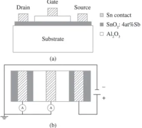
The heterojunctions Al2O3/SnO2 were obtained by deposition of aluminum thin ilms on top of SnO2 ilm, through a shadow mask, and subsequent oxidation to aluminum oxide during thermal annealing. This assembly was used to build a simple device, which was used for electrical characterization. For Al2O3/undoped SnO2, several aluminum layers were deposited, and after each layer the sample was submitted to thermal annealing at 500 °C for 1 hour in O2-rich atmosphere. This sample was called here DU. In the case of Al2O3/Sb-doped (4at%) SnO2 with 2 layers of alumina the annealing time was of 16 h for the two layers for the devices D1 and D2, whereas the time was 24 h for the two layers of the device D3, all annealing carried out at 550 °C, in room atmosphere, where the required time is longer. Sn metallic layers were deposited as electrical contacts for the three terminals (source, drain and gate) of the heterojunction, resulting in a device as shown in Figure 1. The electrical connections for measurements of current as function of voltage (I×V) are also shown in Figure 1.
X-ray diffraction (XRD) data was collected in a Rigaku D/Max – 2100PC equipment at room temperature, using CuKα radiation and beam incident angle of 1.5° to the ilm surface from 20 to 80o with rate of 1o/min. Current and voltage were 20mA and 40KV, respectively. UV-Vis transmittance was obtained with a Perkin Elmer Lambda 1050 equipment in the range 200 to 1000nm. Raman spectroscopy was done by excitation with the 488nm line of a Ar+ laser of Spectra-Physics, model Stabilite 2017 with magnification of 50 times and power 5mW. The monochromator for the Raman signal was a Jobin Yvon T64000. Scanning electron microscopy (SEM) and energy dispersive X-ray spectroscopy (EDX) were carried out with a Quanta 2000 equipment, set with thermionic emitter and a detector Oxford (for EDX).
Current as function of temperature measurements were carried out under vacuum conditions, in a closed helium circuit cryostat of Janis Research, coupled with a Lake
Shore Cryotronics temperature controller with 0.05 degree of precision. The source-drain current were measured with an Agilent Multimeter model 34401A, whereas the source-gate (leakage current) were measured with a Keithley Electrometer model 6517A.
3. Results and Discussion
The electrical characterization evaluated through electrical resistance data for several temperatures, is shown in Figure 2, for a device built according to the diagram shown is Figure 1, with four (4) alumina layers treated at O2-rich atmosphere on the gate, and where SnO2 layer is undoped. The plotted resistance values are related to the two possible conduction channels in the device: source-drain, through the SnO2 conduction channel, and source-gate, which means the leakage current. The characterization of a heterojunction sample of undoped SnO2/Al2O3 with only one layer of alumina in the gate, leads to similar current magnitudes for source-drain and source-gate. However, when the number of layers is increased to 4, the magnitude of the resistance is about 4×10⁸ ohms for the source-gate and 1.3×10⁶ ohms for the source-drain, which means that only 0.3% of the current is lost through the gate as leakage current. The evaluated leakage current is about 10–10 A/ cm2 at zero bias, which is comparable to the system Al
2O3/ GaAs[14]. However, this value was obtained with the device on operation and the current source-drain through the SnO2 conductive channel is only about three orders of magnitude lower. The inset in Figure 2, show the relative resistance of source-drain to source-gate and the tendency is similar to the behavior of absolute value illustrated in main Figure 2. The sole exception is the point at 250K. The general tendency means that as the temperature increases, the source drain channel becomes much more conductive compared to the leakage current through the gate. It is an interesting result toward the production of electronic devices, which in general is designed to work about room temperature. The temperature dependent behavior of the resistance ratio drain/ gate is related to the temperature-dependent electron capture in the semiconductor layer, leading to a resistivity increase
in the SnO2 ilm as the temperature decreases and then, to a value close to unity about 100 K, which means that the concurrent and parallel current paths becomes comparable. At 250K, this ratio deviates from the observed tendency and the ratio value is not as low as expected, suggesting that the Sn electrode deposited on the SnO2 ilm may be playing a different role in this temperature20. It is interesting to mention that 200-250 K is in the temperature range where the capture by defects is mostly active, including trapping by oxygen vacancies21,22, which is very relevant because these samples are not doped. Then, the depletion layer close to the interface metal-semiconductor may be inluenced by the electron trapping by oxygen vacancies, which does not affect the device performance when the temperature is additionally decreased, because the interfacial layer is completely depleted and the overall resistivity is higher.
The importance of this result is signiicantly increased by taken into account that the SnO2 ilm is undoped and the conductivity of the conduction channel source-drain is not high (σ = 0.5 S.cm–1). The conductivity can be signiicantly increased by a doping procedure with a pentavalent doping ion such as Sb+5[23]. The deposition of Al
2O3, leads to a porous material, and then, it may lead to direct metallic contact between SnO2 ilm and the Sn electrode layer. However, the deposition of a series of layers inhibits the percolation of pores, and a better insulation in the gate is obtained. This alumina layer insulation indicates that this procedure for Al2O3 layer deposition may be used for production of transparent ield effect devices. There is a clear indication that an alumina multilayer deposition procedure must lead to a very eficient electrical insulation, with very low leakage current, for samples submitted to short annealing time in O2-rich atmosphere. Besides, the n-type doping of the SnO2 ilm may improve the current magnitude through the semiconductor layer, making the device very useful.
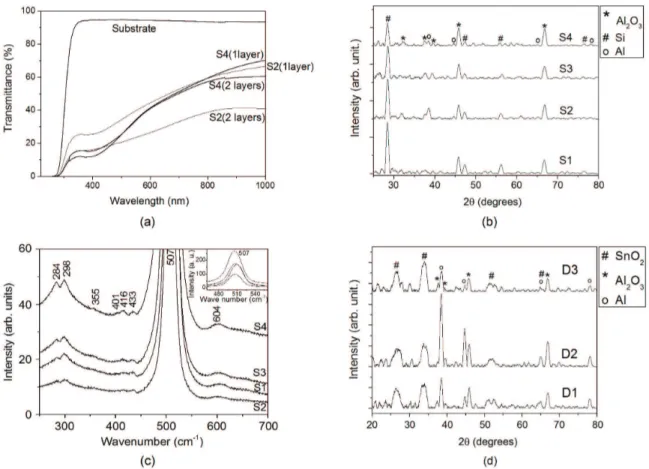
In order to fully understand the role of thermal annealing to the aluminum oxidation, samples were deposited on soda-lime glass substrates and submitted to distinct annealing procedures. After oxidized, samples with one or two alumina layers were submitted to different characterization techniques, with results shown in Figure 3. Figure 3a shows the difference in optical transmittance between samples with one and two alumina layers. In both cases the observed transmittance refers to fully oxidized aluminum layers, with transparency greatly increased when compared to non-oxidized metallic ilm. The ilm is non-oxidized in situations previously to any annealing or when submitted to non-efficient thermal annealing procedure. It must be mentioned that by the procedure used here, oxidized samples needs about 16 h of annealing time in air whereas sample oxidized in O2-rich atmosphere needs only 2 h for complete oxidation. In both cases the annealing temperature is 550 °C[16]. As can be seen in Figure 3a, increasing the number of layers, there is a decrease in the ilm transparency (which is mainly evident for sample S2).
Previously to any TA, as-deposited aluminum is in the FCC crystalline structure (ile number 89-2769 of the catalog JCPDS-ICDD 2003). Figure 3b concerns X-ray diffractogram of two thermally annealed Al2O3 ilms. The sequence of annealing for the two layers of samples S1, S2,
S3 and S4 was described in the Experimental section. After thermal annealing it is possible to notice the oxidation in the diffractogram (Figure 3b). Aluminum oxide found after annealing is γ-alumina, with spinnel structure (JCPDS-ICDD 2003 number 77-0396). It is also possible to found crystalline Si, with FCC structure (JCPDS-ICDD 2003 number 27-1402). This Si layer comes from the soda-lime glass substrate, where Si diffuses to the interface with the Al ilm16. It is similar to what happens in the AIC (aluminum-induced crystallization) technique, for Si deposition24,25, where the silicon nucleates on the Al surface.
Figure 3c shows Raman data for thermally oxidized Al layers and show characteristic Al-O vibrations of γ-alumina26. Vibrations related to α-alumina are also present even though in less proportion when compared to γ-alumina. FTIR results16 are in good agreement with Raman data, presenting characteristic vibration of aluminum oxide. In Figure 3c, the most intense peak is shown about 507cm–1, and although it may be related to alumina, most probably it can be associated to crystalline silicon27,28. In this case, the Si would be originated from the substrate24,25, diffusing to the interface substrate/Al, as discussed before, in good agreement with some peaks found out the XRD diffractograms.
Figure 3d shows X-ray diffractograms for Al2O3 ilms deposited on Sb-doped SnO2 layers. It is observed
a lower oxidation in the Al ilms compared to the same ilms deposited on soda-lime glass substrate, shown in Figure 3b. Although the TA is the same, for the Al2O3/SnO2 the diffractogram still present peaks related to metallic aluminum with CFC structure and therefore, the oxidation to alumina is partial. Besides, unlike deposition of Al on soda-lime glass, Si peaks are absent in this case. It is in good agreement with the explanation of Si diffusion from the glass substrate to the interface, because in this case, there is no contact between the Al layer and the soda-lime glass substrate as the SnO2 intermediate layer avoids the Si diffusion.
In order to reinforce the XRD and Raman results shown in Figure 3, the composition of each sort of sample was analyzed by EDX. Table 1 lists the relative chemical composition (in weight) of the samples of Al2O3 deposited on soda-lime substrates and Al2O3 deposited on SnO2 thin ilms. It can be observed that there is a higher Si concentration in the sample deposited on the soda-lime glass substrate compared to the sample Al2O3/SnO2, in good agreement with the Si ilm formation in the irst case. The higher oxygen concentration for the sample Al2O3/SnO2 refers to the deposition of two distinct oxide layers, along with the avoiding of Si layer growth, which also contributes for the decrease of the Si concentration in this sample. Si and other elements such as Na, K and Ca were found in EDX and
Figure 3. (a) Transmittance in the UV-Vis-IR spectra for 2 alumina layer, (b) XRD of 2 alumina layer after TA, (c) Raman of 1 alumina
belong to the soda-lime glass composition. Besides, there is a high percentage of Au due to its utilization for metallization needed in scanning electron microscopy (SEM) procedure. Figure 4 shows some electrical properties of 4at%Sb-doped SnO2 ilm. Resistivity as function of temperature is measured in the dark and after illumination for 6 min at several distinct temperatures with an InGaN LED of wavelength about 450nm. The photo-excitation is an interesting result, because the device proposed here is transparent, with potential use in Optoelectronics. The overall conductivity is not very high due to small crystallites, even though the free electron concentration is elevated29. The inset in Figure 4 shows the relative variation in the resistivity after irradiation at each temperature. The illumination increases the sample conductivity, even though the energy is below the SnO2 bandgap (corresponding to wavelength of about 350nm) and, then, electron-hole pair excitation does not take place. The increase in conductivity is a long duration effect, which is only destroyed for heating the sample until room temperature. It is interesting to notice that the least photo-induced excitation takes place about 200 K, in agreement with the evaluation of relative resistance of source-drain to source-gate (Figure 2), because at 250K, this ratio deviates from the observed tendency and is not as low as expected. Besides the possible Sn electrode inluence, it is interesting to recall that 200-250 K is the temperature range where the capture by defects is mostly active, including trapping by oxygen vacancies21,22. In the case of 4at%Sb-doped SnO2, reported in Figure 4, the least excitation is
Table 1. Chemical composition (in weight) of the samples of Al2O3/ soda-lime substrate and Al2O3/SnO2 obtained from EDX results.
Element On top of soda
lime glass (wt%)
On top of SnO2 (wt%)
O 21.9 24.3
Al 17.7 14.0
Si 18.9 11.8
Sn - 12.2
Other 41.5 37.8
Figure 4. Resistivity as function of temperature for 4at%Sb-doped SnO2 ilm in the dark and after excitation for 6 min at different
temperatures with an InGaN LED (λ about 450nm). Inset: relative
variation of resistivity for photo-excitation at each temperature.
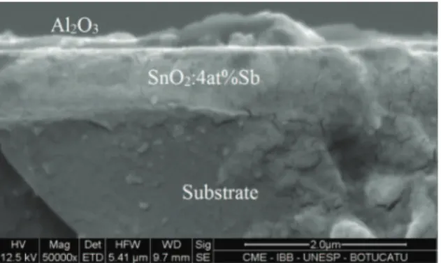
Figure 5. SEM of heterojunction Al2O3/Sb-doped SnO2 thermally annealed in air at 550 °C for 24 h, for each of the 2 alumina layers. about 200 K, suggesting a poor optical ionization of defects, in this case Sb-centers must be added to oxygen vacancies. Besides, the highest photo-excitation takes place for room temperature, which is also an interesting result toward the design and production of transparent electronic devices, in good agreement to the relative resistance of source-drain to source-gate, shown for the undoped SnO2/Al2O3 sample, shown in Figure 2.
Although the Sb-doped film has semiconducting properties, reported on Figure 4, unlike data for undoped SnO2/Al2O3 the Sb-doped SnO2 /Al2O3 heterojunction, assembled by the simple device shown in Figure 1, presented the source-gate current higher than the source-drain, which was an unexpected and undesired result. The long annealing time in atmospheric condition, 16 h and 24 h at 550 °C, for the 2, 3 and 4 layers for the devices D1, D2 and D3, respectively, needed for the complete aluminum oxidation to alumina, probably caused this situation, due to interdiffusion of metallic ions between semiconductor/insulating layers and a higher degradation of the whole device. Nevertheless, the higher number of alumina layers increases 20 times the electrical resistance of the alumina coating when four layers are deposited, but the source-gate channel still presents lower resistance than the source-drain channel. The XRD difratograms (Figure 3d) are in good agreement with this result, since it does not show an eficient oxidation of the alumina layer when it is deposited on SnO2 ilms. Besides, it increases its roughness and non-uniformity as observed by confocal microscopy (not shown) and SEM, as will be seen below. Comparing the eficiency of oxidation process of thermal annealing in different atmospheres, it may be concluded that the alumina must be obtained by oxidation of aluminum in O2-rich atmosphere conditions, where the short time required allows an eficient oxidation and low leakage current. Besides, it avoids the degradation of the device quality caused by long annealing times.
the SnO2 layer seems to be 750nm thick. This thickness is much higher when compared to SnO2 layer grown separately on borosilicate glass substrate by the same procedure, with a inal thermal annealing of 1h at 550 °C and 10 layers30, suggesting that the alumina layer shown in Figure 5 is swelled by interdiffusion of metallic ions. This is in good agreement with the poor insulating role of the alumina layer in the device, when the alumina is treated for a long time, justifying the probable presence of aluminum oxides nuclei in the conduction channel.
4. Conclusion
Combining the transparent semiconducting properties of SnO2 thin ilms with the insulating properties of Al2O3 leads to a potentially applicable heterojunction. The simple device assembled here shows that the insulation depends on the number of layers deposited and on the time of thermal annealing, which must be short to avoid degradation of the alumina layer, recommending the use of O2-rich atmospheres. For single layers, the possible existence of pores has led to a source–gate current comparable to source– drain current, in this case the contact between SnO2 and the Sn electrode is practically independent on the existence of an intermediate alumina layer. A similar result is obtained for multi-layered alumina with long thermal annealing in room atmosphere. In the case of the heterojunction of undoped SnO2 and Al2O3 (where the Al layers were treated under
O2-rich atmosphere), when the number of alumina layers is four, the insulation increased signiicantly, suggesting that the deposition of more alumina layers led to much less percolated pores. The relative resistance of the conduction channel compared to the resistance of the channel through the gate terminal decreases signiicantly with number of layers and with increasing temperature, suggesting the use of this device at room temperature.
Besides aluminum oxide on spinnel structure, it was also found Si in the interface with Al ilm in the thermally treated layers, deposited on glass substrates.
The formation of SnO2/Al2O3 heterojunction, with alumina layer obtained from deposited Al layer with thermal annealing, may be seen as a potential technique for application in transparent transistor production, mainly due to its simplicity. Beside the low leakage current, the transparent characteristic of the whole device allow the interaction with light, mainly at room temperature, and the use in Optoelectronics.
Acknowledgements
The authors would like to thank Prof. A. Tabata, for the Raman data, and the inancial support of the Brazilian agencies: CNPq, FAPESP and FUNDUNESP (grant 91312/13-DFP). XRD and UV-VIS-NIR were performed at Multiuser Laboratory at UNESP/DF Campus Bauru.
References
1. Kingon AI, Maria JP and Streiffer SK. Alternative dielectrics to silicon dioxide for memory and logic devices. Nature. 2000; 406(6799):1032-1038. http://dx.doi.org/10.1038/35023243. PMid:10984062
2. Robertson J. High dielectric constant gate oxides for metal oxide Si transistors. Reports on Progress in Physics. 2006; 69(2):327-396. http://dx.doi.org/10.1088/0034-4885/69/2/R02.
3. Lin CC and Hwu J-G. Nitric acid compensated aluminum oxide dielectrics with improved negative bias reliability and positive bias temperature response. Journal of Applied Physics. 2013; 113(5):054103. http://dx.doi.org/10.1063/1.4790371.
4. Chiang J-C and Hwu J-G. Low temperature (<400 °C) Al2O3 ultrathin gate dielectrics prepared by shadow evaporation of aluminum followed by nitric acid oxidation. Applied
Physics Letters. 2007; 90(10):102902. http://dx.doi.
org/10.1063/1.2711290.
5. Kim S, Nah J, Jo I, Shahrjerdi D, Colombo L, Yao Z, et al. Realization of a high mobility dual-gated graphene field-effect transistor with Al2O3 dielectric. Applied Physics Letters. 2009; 94(6):062107. http://dx.doi.org/10.1063/1.3077021.
6. Woo CH, Ahn CH, Kwon YH, Han J-H and Cho HK. Transparent and flexible oxide thin-film-transistors using an aluminum oxide gate insulator grown at low temperature by atomic layer deposition. Metals and Materials International. 2012; 18(6):1055-1060. http://dx.doi.org/10.1007/s12540-012-6020-5.
7. Ha HJ, Jeong SW, Oh T-Y, Kim M, Choi K, Park JH, et al. Flexible low-voltage pentacene memory thin-film transistors with combustion-processable Al2O3 gate dielectric and Au nanoparticles. Journal of Physics. D, Applied Physics.
2013; 46(23):235102. http://dx.doi.org/10.1088/0022-3727/46/23/235102.
8. Jeurgens LPH, Sloof WG, Tichelaar FD and Mittemeijer EJ. Structure and morphology of aluminum-oxide films formed by thermal oxidation of aluminum. Thin Solid Films. 2002; 418(2):89-101. http://dx.doi.org/10.1016/S0040-6090(02)00787-3.
9. Xuan Y, Lin HC, Ye PD and Wilk GD. Capacitance-voltage studies on enhancement-mode InGaAs metal-oxide-semiconductor field-effect transistor using atomic-layer-deposited Al2O3 gate dielectric. Applied Physics Letters. 2006; 88(26):263518. http://dx.doi.org/10.1063/1.2217258.
10. Lin HC, Ye PD and Wilk GD. Current-transport properties of atomic-layer-deposited ultrathin Al2O3 on GaAs.
Solid-State Electronics. 2006; 50(6):1012-1015. http://dx.doi.
org/10.1016/j.sse.2006.04.021.
11. Hong-Wen L, Hong Z, Xue-Min W, Yan Z, Da-Wei Y, Zhong-Qian J, et al. Measurement of ZnO/Al2O3 Heterojunction Band Offsets by in situ X-Ray Photoelectron Spectroscopy.
Chinese Physics Letters. 2013; 30(11):118201. http://dx.doi.
org/10.1088/0256-307X/30/11/118201.
12. Yao J, Zhang S and Gong L. Band offsets in ZrO2/InGaZnO4 heterojunction. Applied Physics Letters. 2012; 101(9):093508. http://dx.doi.org/10.1063/1.4750069.
13. Serin T, Serin N, Karadeniz S, Sari H, Tuğluoğlu N and Pakma O. Electrical, structural and optical properties of SnO2 thin films prepared by spray pyrolysis. Journal of Non-Crystalline
Solids. 2006; 352(3):209-215. http://dx.doi.org/10.1016/j.
jnoncrysol.2005.11.031.
on GaAs. Applied Physics Letters. 2005; 87(18):182904. http:// dx.doi.org/10.1063/1.2120904.
15. Kirsch PD, Kang CS, Lozano J, Lee JC and Ekerdt JG. Electrical and spectroscopic comparison of HfO2/ Si interfaces on nitrided and un-nitrided Si.100. Journal of Applied Physics. 2002; 91(7):4353. http://dx.doi.org/10.1063/1.1455155. 16. Boratto MH and de Andrade Scalvi LV. Deposition of
Al2O3 by resistive evaporation and thermal oxidation of Al to be applied as a transparent FET insulating layer.
Ceramics International. 2014; 40(2):3785-3791. http://dx.doi.
org/10.1016/j.ceramint.2013.09.041.
17. Bagheri-Mohagheghi MM and Shokooh-Saremi M. The influence of Al doping on the electrical, optical and structural properties of SnO2 transparent conducting films deposited by the spray pyrolysis technique. Journal of Physics. D,
Applied Physics. 2004; 37(8):1248-1253. http://dx.doi.
org/10.1088/0022-3727/37/8/014.
18. Yamazoe N, Fuchigami J, Kishikawa M and Seiyama T. Interaction of tin oxide surface with O2, H2O and H2. Surface
Science. 1979; 86:335-344.
http://dx.doi.org/10.1016/0039-6028(79)90411-4.
19. Geraldo V, Briois V, Scalvi LVA and Santilli CV. Structural Characterization of Nanocrystalline Sb-Doped SnO2 Xerogels by Multiedge X-ray Absorption Spectroscopy. The Journal of
Physical Chemistry C. 2010; 114(45):19206-19213. http://
dx.doi.org/10.1021/jp106001x.
20. Maciel JLB, Floriano EA, Scalvi LVA and Ravaro LP. Growth of Al2O3 thin films by oxidation of resistively evaporated Al on top of SnO2, and electrical properties of the heterojunction SnO2/Al2O3. Journal of Materials Science. 2011; 46(20):6627-6632. http://dx.doi.org/10.1007/s10853-011-5613-6.
21. Morais EA and Scalvi LVA. Electron trapping of laser-induced carriers in Er-doped SnO2 thin films. Journal of the European
Ceramic Society. 2007; 27(13-15):3803-3806. http://dx.doi.
org/10.1016/j.jeurceramsoc.2007.02.037.
22. Samson S and Fonstad CG. Defect structure and electronic donor levels in stannic oxide crystals. Journal of Applied Physics. 1973; 44(10):4618. http://dx.doi.org/10.1063/1.1662011.
23. Shanthi E, Dutta V, Banerjee A and Chopra KL. Electrical and optical properties of undoped and antimony-doped tin oxide films. Journal of Applied Physics. 1980; 51(12):6243. http:// dx.doi.org/10.1063/1.327610.
24. Nast O, Brehme S, Pritchard S, Aberle AG and Wenham SR. Aluminium-induced crystallization of silicon on glass for thin-film solar cells. Solar Energy Materials and Solar Cells. 2001; 65(1-4):385-392. http://dx.doi.org/10.1016/S0927-0248(00)00117-3.
25. Wang T, Yan H, Zhang M, Song X, Pan Q, He T, et al. Polycrystalline silicon thin films by aluminum induced crystallization of amorphous silicon. Applied Surface
Science. 2013; 264:11-16. http://dx.doi.org/10.1016/j.
apsusc.2012.09.019.
26. Thomas PV, Ramakrishnan V and Vaidyan VK. Oxidation studies of aluminum thin films by Raman spectroscopy.
Thin Solid Films. 1989; 170(1):35-40. http://dx.doi.
org/10.1016/0040-6090(89)90619-6.
27. Wang W, Huang J, Lu Y, Yang Y, Song W, Tan R, et al. In situ micro-Raman spectroscopic study of laser-induced crystallization of amorphous silicon thin films on aluminum-doped zinc oxide substrate. Journal of Materials Science Materials in Electronics. 2012; 23(7):1300-1305. http://dx.doi. org/10.1007/s10854-011-0588-2.
28. Huang Y, Law F, Widenborg PI and Aberle AG. Crystalline silicon growth in the aluminium-induced glass texturing process. Journal of Crystal Growth. 2012; 361:121-128. http:// dx.doi.org/10.1016/j.jcrysgro.2012.09.015.
29. Geraldo V, Scalvi LVA, Lisboa-Filho PN and Morilla-Santos C. Drude’s model calculation rule on electrical transport in Sb-doped SnO2 thin films, deposited via sol–gel. Journal of Physics and Chemistry of Solids. 2006; 67(7):1410-1415. http:// dx.doi.org/10.1016/j.jpcs.2006.01.102.
30. Geraldo V, Scalvi LVA, Morais EA, Santilli CV and Pulcinelli SH. Sb doping effects and oxygen adsorption in SnO2 thin films deposited via sol-gel Materials Research. Ibero American