324 Brazilian Journal of Physics, vol. 36, no. 2A, June, 2006
Characterization of SnTe Films Grown by Molecular Beam Epitaxy
U. A. Mengui, E. Abramof, P. H. O. Rappl, and A Y. Ueta
Instituto Nacional de Pesquisas Espaciais – INPE, Laborat ´orio Associado de Sensores e Materiais - LAS, Caixa Postal 515, 12245-970, S˜ao Jos´e dos Campos - SP, Brazil.
Received on 4 April, 2005
A series of SnTe layers with thicknesses varying from 0.42 to 9.1 µm were grown by molecular beam epitaxy on (111) BaF2substrates. The SnTe lattice parameter was found to be 6.331 ˚A as determined from x-ray dif-fraction spectra measured in the triple-axis configuration. The FWHM of the (222) SnTe x-ray rocking curves indicated a good crystalline quality and an unusual dependence on layer thickness. Atomic force microscopy (AFM) of the SnTe surface revealed spirals with monolayer steps formed around threading dislocations, sim-ilar to the PbTe on BaF2 epitaxy. The dislocation density was estimated from the AFM picture to be 9x108 cm−2. Small black pits corresponding to holes that were left during growth were also observed on the AFM images. Sn diffusion can be a possible reason for these pits and the relatively high dislocation density. Electrical measurements showed that the SnTe epilayers present a typical p-type carrier concentration around 1020cm−3 almost temperature independent and a Hall mobility which decreases from 104to 103cm2/V.s as the temperature increases from 10 to 350K.
Keywords: SnTe; Molecular beam epitaxy; BaF2substrates
I. INTRODUCTION
SnTe is an IV-VI narrow gap semiconductor that crystal-lizes in the rock salt structure and whose optical and electri-cal properties have been investigated since the beginning of 1960’s [1-3]. This kind of compound finds application in the construction of thermoelectric generators and infrared detec-tors [4-5]. The study of structural properties of IV-VI com-pounds related to misfit and threading dislocations in systems like PbTe, PbSe and PbTe1−xSexdeposited on different sub-strates, such as KCl, BaF2, Si and PbSe have been done by
several groups [6-10].
We investigate here the structural and electrical properties of a series of SnTe films with different thicknesses grown by molecular beam epitaxy on (111) BaF2substrates.
High-resolution x-ray diffraction and atomic force microscopy ap-plied to the grown samples allowed the determination of structural parameters like lattice constant, crystalline quality, threading dislocation density and surface morphology. Hall concentration and mobility were determined as a function of temperature for the different SnTe films.
II. EXPERIMENTAL PROCEDURES
For this investigation, a series of SnTe films was grown on freshly cleaved (111) BaF2substrates by molecular beam
epi-taxy in a Riber 32P MBE system. Prior to growth, the sub-strates were preheated at 200oC during 30 min, in the prepa-ration chamber, and at 500 oC during 15 min, in the main chamber. The layers were grown from a SnTe stoichiometric solid source. The substrate and SnTe effusion cell tempera-tures were kept constant during growth at 320oC and 676oC, respectively, and the deposition time was varied from 0.5 to 9 h. The mean value of growth rate was found to be 0.9 µm/h. The substrate holder was kept rotating to insure a reasonable thickness homogeneity for all samples.
A 12 keV reflection high energy electron diffraction
(RHEED) system was used to monitor in situ the growths. After the opening of the SnTe cell shutter, the RHEED pattern immediately changes to the one characteristic of three-dimensional island formation, indicating Volmer-Weber growth mode. Subsequently, as the islands start to coalesce, the RHEED diffraction pattern changes to a streaked one and persists until the end of growth.
The thickness of the SnTe layers were determined with an Alpha Step 500 DekTak profilometer after an etch step to re-move a small part of the film. The SnTe samples were struc-turally characterized by high-resolution x-ray diffraction mea-surements carried out in a Philips X’Pert diffractometer us-ing CuKα1radiation. A four-crystal Ge(220) monochromator
is positioned in front of the x-ray tube, leading to an inci-dent beam with an axial divergence of 12 arcsec and a wave-length dispersion of approximately 2x10⁻⁴. The diffracted beam can go directly to the detector with an aperture of 1o (open-detector configuration) or pass through a channel-cut analyzer placed in front of the detector, which reduces the de-tector acceptance to 12 arcsec (triple-axis configuration). An atomic force microscope (AFM) SPM2-Shimadzu operated in contact mode was used for topographical images. Finally, an automated Keithley 180A Hall effect system was used to mea-sure the electrical properties of the samples contacted in the Van der Pauw geometry. Resistivity and Hall measurements were performed at temperature varying from 10 to 350K.
III. RESULTS AND DISCUSSIONS
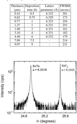
We first measured theω/2Θscans around the (222) Bragg diffraction peak of both film and substrate of all samples with the x-ray diffractometer in the triple-axis configuration. Fig. 1 shows, as an example, the x-ray diffraction spectrum of the SnTe sample with a film thickness of 1.6 µm. The (222) Bragg peak of the SnTe film and BaF2substrate are clearly seen in
sub-U. A. Mengui et al. 325
strate peak as a reference. The SnTe lattice parameter of al-most all samples is displayed in Table I, presenting a mean value of 6.331 ˚A.
TABLE I: Data of the SnTe samples as obtained from growth para-meters, profilometry and x-ray analysis.
Thickness Deposition Lattice FWHM (µm) time (h) parameter ( ˚A) (arcsec)
0.42 0.5 6.332 201
0.62 0.75 6.329 173
0.77 1 6.333 254
1.27 1 6.331 251
1.60 2 6.331 161
3.10 4 6.331 182
4.40 6 6.332 179
7.09 7.5 - 214
9.07 9 - 231
FIG. 1:ω/2Θscan measured around the (222) Bragg diffraction peak for a SnTe/BaF2sample with thickness of 1.6 µm.
In order to investigate the crystalline quality of the grown layers, we measured the rocking curves in the vicinity of the SnTe (222) Bragg reflex. The rocking curve is aω-scan with the open detector fixed at the desired 2Θ Bragg angle. The full-width at half-maximum (FWHM) of the rocking curve is very sensitive to threading dislocations and defects present in the film, and can be considered as a measure of the crystalline quality. The FWHM obtained for all samples is also shown in Table I, and Fig. 2 plots its dependence on the layer thickness. The FWHM varies in a range from 160 to 250 arcsec for layer thickness between 0.4 and 2.0 µm, and increases monotoni-cally from 160 to 230 arcsec as the layer increases its thick-ness until 9 µm. This behavior is opposed to what is expected for this type of epitaxial layer, as in the case of PbTe on BaF2,
in which the density of threading dislocations, and hence the FWHM, decreases as the film becomes thicker [7]. We think that Sn diffusion may be one reason to explain this unusual
behavior. Since Sn diffusion coefficient is higher in compar-ison, for instance, with the Pb one, the diffusion of Sn atoms during growth may lead to other type of defects that may be responsible for the rise in the FWHM values. This is espe-cially important at relatively high growth temperatures.
FIG. 2: Full-width at half-maximum of the (222) SnTe x-ray rocking curves as a function of layer thickness.
In order to get a better insight in this problem, we inves-tigated the surface of the SnTe layers with atomic force mi-croscopy. Fig. 3 shows the AFM image of a SnTe layer with a thickness of 7.09 µm. The scanned area is 5x5 µm2. One can clearly observe the spirals with monolayer steps near the threading dislocations, similar to the PbTe on BaF2 growth.
Spiral growth AFM images have been reported for PbTe grown by MBE on BaF2substrate [7,11]. It was shown that
PbTe growth is totally dominated by spirals formed around threading dislocations that originate from the 4.2% lattice mismatch to the substrate. It is important to remind that due to the heteroepitaxy of a thin film on lattice-mismatched sub-strate, growth spirals normally appear as a consequence of the high density of threading dislocations formed during the strain relaxation process [12-13]. As shown in the picture of Fig. 3, the SnTe film surface actually presents a mound for-mation with spiral shape. The SnTe spiral heights are some few monolayer steps, and the surface of this film as a whole can be considered very smooth. We can also conclude that a pure step flow growth mode occurs in the SnTe/BaF2system,
where the deposition of adatoms results in a lateral growth at the step edges.
Both ends of the short segments of monolayer steps are ter-minated by a threading dislocation, originated from the 2% lattice mismatch between SnTe and BaF2. Considering this
fact, the density of dislocations can be estimated from the AFM image in Fig. 3. A value of 9x108cm−2is found for the 7.09 µm thick SnTe film, which is much higher than 5x10⁶
cm−2 reported for PbTe/BaF
2film with equivalent thickness
326 Brazilian Journal of Physics, vol. 36, no. 2A, June, 2006
4.39 [nm]
0.00
2.00 um 5.00 x 5.00 um
0 E H
FIG. 3: AFM image of a 7.09 µm thick SnTe layer grown on (111) BaF2substrate.
during growth. We believe that Sn diffusion may be the rea-son for these pits and also for the higher density of threading dislocations, which lead to the relatively high FWHM values observed here in the SnTe x-ray rocking curves.
The electrical properties of the SnTe films were also mea-sured as function of temperature from 10 to 350K. As for the bulk crystals, the SnTe films exhibited a high hole concen-trations around 1020 cm−3, as shown in Fig. 4a. The strong p-type character comes from the SnTe phase diagram, which solubility is only restricted to the Te-rich region. The car-rier concentration has almost no temperature dependence, as predicted from the vacancy model, showing no carrier frozen. These p values are in agreement with those reported in the literature [14-16], where the lowest hole concentration ob-tained for SnTe films grown by MBE was 1019 cm−3using special growth conditions [16] or Bi doping, which is an n-type dopant [14]. Fig. 4b shows the mobility of the SnTe films with different thickness as a function of temperature. For most of the films, the mobility decreases from 104to 103cm2/V.s as the temperature increases from 10 to 350K. Phonon scatter-ing is the main mechanism responsible for this behavior. The graph in Fig. 4b also shows that thicker SnTe films exhibited higher mobility, as expected.
IV. CONCLUSION
A lattice parameter of 6.331 ˚A was found for the SnTe lay-ers grown by MBE on BaF2substrates. The FWHM of the
(222) SnTe x-ray rocking curves exhibited an unusual depen-dence on layer thickness. The AFM image of the SnTe surface revealed spirals with monolayer steps formed around thread-ing dislocations, similar to the PbTe on BaF2epitaxy. Black
10 100
1020
(a)
p (cm
-3
)
Temperature (K)
0,62 µm1,27 µm
4,40 µm
7,09 µm
9,07 µm
10 100
102 103 104
(b)
µ
(cm
2
/V
.s)
Temperature (K)
0.62 µm1.27 µm
4.40 µm
7.09 µm
9.07 µm
FIG. 4: Hole concentration (a) and Hall mobility (b) versus temper-ature for SnTe films with different thicknesses.
pits corresponding to holes created during growth were also observed on the AFM pictures. We believe that Sn diffusion may be a reason for these pits and also for the relatively high dislocation density found in the SnTe films. The carrier con-centration and the Hall mobility measured for the SnTe epi-taxial layers presented the expected temperature dependence and values.
Acknowledgement
The authors thank ITA/CTA in S˜ao Jos´e dos Campos, SP, Brazil, for the use of their AFM equipment. U. A. Mengui would like to thank CAPES and CNPq for financial support
[1] M. Cardona and D. L. Greenaway, Phys. Rev. 133 (6A), A1685 (1964).
U. A. Mengui et al. 327
Rev. Lett. 14 (10), 360 (1965).
[3] J. N. Zemel, J. D. Jensen, and R. B. Schoolar, Phys. Rev. 140 (1A), A330 (1965).
[4] G. J. Snyder, Appl. Phys. Letters 84 (13), 2436 (2004). [5] G. Scott, C.R. Helms, J. Vacuum Science & Technology B 9
(3): 1785-1788 (1991).
[6] A. I. Fedorenko, O. N. Nashchekina, B. A. Savitskii, L. P. Sh-pakovskaya, O. A. Mironov, and M. Oszwaldowski, Vacuum 43 (12), 1191 (1992).
[7] G. Springholz, A. Y. Ueta, N. Frank, and G. Bauer, Appl. Phys. Lett. 69 (19), 2822 (1996).
[8] P. M¨uller, H. Zogg, A. Fach, J. John, C. Paglino, A. N. Ti-wari, M. Krejci, and G. Kostorz, Phys. Rev. Lett. 78 (15), 3007 (1997).
[9] H. Z. Wu, S. M. Fang, R. Salas Jr., D. McAlister, and P. J.
McCann, J. Vac. Sci. Technol. B 17 (3), 1263 (1999).
[10] K. Wiesauer and G. Springholz, Phys. Rev. B 69, 245313 (2004).
[11] A. Y. Ueta, G. Springholz, and G. Bauer, J. Cyst. Growth 175, 1022 (1997).
[12] J. Y. Tsao, Materials Fundamentals of Molecular Beam Epitaxy (Academic, London, 1993).
[13] J. W. Matthews, in Dislocation in Solids, edited by F. R. N. Nabarro (North-Holland Publ. Co, 1979).
[14] M. A. Tamor, H. Holloway, R. M. Ager, C. A. Gierczak, and R. O. Carter, J. Appl. Phys. 61 (3), 1094 (1987).
[15] A. B. Mandale, Materials Lett. 9, 389 (1990).