UNIVERSIDADE DA BEIRA INTERIOR
Engenharia
Fault Tolerant DC-DC Converters
Fernando José Figueiredo Bento
Dissertação para obtenção do Grau de Mestre em
Engenharia Eletrotécnica e de Computadores
(2º ciclo de estudos)
Orientador: Prof. Doutor António João Marques Cardoso
UNIVERSIDADE DA BEIRA INTERIOR
Engineering
Fault Tolerant DC-DC Converters
Fernando José Figueiredo Bento
Dissertation for obtaining the degree of Master of Science in
Electrical and Computer Engineering
(2
ndcycle of studies)
Advisor: Prof. Dr. António João Marques Cardoso
Acknowledgments
This work was just possible due to the contribution and effort of many people, that I would like to acknowledge. First of all, I want to thank to all my family, specially my parents, brothers and grandmother, for the support given during this long journey.
I would like to demonstrate my deep gratitude to my Master Dissertation advisor, Prof. Dr. António João Marques Cardoso, for the supervision and for providing workspace and laboratory equipment that allowed me to successfully accomplish this work.
I would like to thank to all my teachers and university colleagues for the knowledge and experiences shared along these five years. Without them, I would not be able to reach this level.
I also wanted to leave a consideration word to all the members of CISE - Electromechatronic Systems Research Centre, in particular to Dr. Jorge Estima and Prof. Dr. Davide Fonseca, that promptly helped me in many technical details of my work.
Thanks to my laboratory colleagues and friends Maria, Saúl, and Waled for the company and help provided throughout this year.
Finally, I want to thank to all my friends, with a special thanks to Serafim and Tiago Machado, for all the advices and company given along my academic career, since I started working on Universidade da Beira Interior.
Resumo
O avanço da tecnologia verificado nos últimos tempos é notório, sobretudo nas cargas utilizadas em nossas casas. Esse avanço trouxe até às nossas habitações novos equipamentos eletrónicos e outras cargas compatíveis com DC, que fazem uma gestão mais eficiente da energia, recorrendo a conversores eletrónicos de potência para esse efeito. Estas cargas têm como denominador comum o facto de necessitarem, em determinado ponto, de retificar para DC a energia AC absorvida da rede elétrica.
Por outro lado, assistiu-se ao crescimento significativo do número de sistemas de micro-geração de energia. A grande maioria destes sistemas produz energia DC.
Estas duas constatações, aliadas à crescente pressão relacionada com a necessidade de sis-temas eficientes em termos energéticos, levarão a que, num futuro próximo, redes DC à escala de bairros sejam implementadas, permitindo assim a ligação de instalações de micro-geração a cargas DC, dentro do mesmo bairro, como uma forma de reduzir o número de passos de conversão de energia, bem como as perdas no transporte dessa energia através de redes AC convencionais. Num futuro em que redes DC serão utilizadas, é essencial a criação de vários níveis de tensão que permitam a ligação dos diferentes tipos de cargas alimentadas a partir de DC. Apenas os conversores eletrónicos DC-DC permitem produzir os diferentes níveis de tensão necessários. A fiabilidade desses conversores torna-se, por isso, num fator de importância ex-trema na continuidade do fornecimento de energia às cargas a eles ligadas e, ao mesmo tempo, na manutenção da qualidade da energia entregue por parte desses conversores a essas mesmas cargas. Com o aumento da fiabilidade destes conversores em mente, este trabalho aplica uma forma de deteção de falhas por circuito aberto nos semicondutores de potência, aplicável em diversas topologias de conversores DC-DC. Após a deteção de uma falha de circuito aberto em qualquer um dos IGBTs do conversor, são realizadas ações de reconfiguração, que não são do mais que alterações no controlo do conversor que permitirão reduzir os impactos dessa falha, como por exemplo o aumento do ripple na corrente. De forma a verificar a efetividade destes métodos, foram efetuados ensaios experimentais, recorrendo a um protótipo do interleaved
DC-DC boost converter de três fases, ligado a uma carga resistiva.
Palavras-chave
Abstract
Technology advancement verified in recent times is flagrant, specially in our home appliances. This advancement brought to us new electronic equipment and other DC-compatible appliances with improved capability for energy management, using electronic converters for such purpose. These loads have in common the fact that, at a certain point, they need to transform the AC energy of the grid to DC.
Furthermore, an important increase in the distributed generation of energy has been wit-nessed. The majority of these systems produce energy in DC.
These two statements, combined with the increased pressure related to the need of energy efficient systems, will certainly trigger, in a near future, the adoption of district-scale DC grids that connect DC generation plants and consumers, in an effort to reduce the number of con-version steps required to deliver power to a DC appliance and, at the same time, limit power losses arising from the energy transportation using conventional AC grids.
In a future where DC grids will be used, several DC voltage levels will be required to allow the connection of the different load profiles that require DC. The inclusion of DC-DC converters will allow the creation of these voltage levels. The reliability of such converters plays a key role, as it ensures service continuity for the DC loads connected to them and, at the same time, preserve the quality of the energy delivered by these converters. With the reliability levels increase as a goal, this work uses an open-circuit fault-diagnostic method suitable for several DC-DC converter topologies. After detecting an open-circuit fault in any of the converter power switches, the control of the converter is re-adapted in order to minimize the adverse impacts of an open-circuit fault, namely the increase of the current ripple. To verify the effectiveness of these strategies, laboratory tests were conducted, using a three-phase interleaved boost converter prototype connected to a resistive load.
Keywords
Index
1 Introduction 1
1.1 Why is DC so Important? . . . 2
1.1.1 DC Loads in our Dwellings . . . 2
1.1.2 Domestic Microgeneration Evolution . . . 4
1.2 Finding the Best Ways to Save Energy . . . 5
1.2.1 Alternative Grid Architectures . . . 5
1.2.2 Last Generation Semiconductors in the State-of-the-Art Power Converters 8 1.3 Loads Susceptibility to Voltage/Current Fluctuations . . . 8
1.4 Previous Studies in the Domain of DC-DC Converters . . . 9
1.4.1 Most Common Components Prone to Failures . . . 9
1.4.2 State-of-the-Art on Open-Circuit Fault Detection and Reconfiguration . . . 10
2 Converter Operation 11 2.1 Converter Control Strategy . . . 11
2.2 Circuit Behaviour under Normal Operation . . . 13
2.3 Circuit Behaviour under Faulty Operation . . . 14
3 Fault Diagnosis 15 4 Converter Reconfiguration After an Open-Circuit Fault 19 4.1 Phase Correction Component . . . 20
4.2 PWM Generation Component . . . 21
5 Simulation Results 23 6 Experimental Set-Up and Results 29 6.1 Experimental Set-Up . . . 29
6.2 Experimental Results . . . 30
7 Conclusions and Suggestions for Future Works 35 7.1 Conclusions . . . 35
7.2 Suggestions for Future Works . . . 35
Bibliography 37
List of Figures
1.1 Average residential electricity consumption by end-use in Europe - 27. . . 2
1.2 Simplified structure of an electronic frequency regulator. . . 4
1.3 Behaviour of a traditional air conditioner vs. air conditioner with VFD. . . 4
1.4 Total installed power related with microgeneration systems. . . 5
1.5 Simplified structure of an electronic frequency regulator supplied with DC. . . . 6
1.6 Power distribution system in a dwelling: (a) Typical structure; (b) Proposed struc-ture. . . 7
2.1 Three-phase interleaved DC-DC boost converter. . . 11
2.2 Average current controller used in the interleaved DC-DC boost converter. . . 12
2.3 Operation of the converter under normal conditions. . . 13
2.4 Operation of the converter after an open-circuit fault in the power switch of phase 1 at t = 0.1 ms. . . . 14
3.1 Basic structure of the fault detection block. . . 16
3.2 PWM pulses, Phase currents, Converter input current, Push into stack and Pop from stack commands for: (a) D < 1/3; (b) 1/3 < D < 2/3. . . . 17
3.3 Fault detection block with delay capability. . . 18
3.4 Pulses that control the push into stack of Iin. . . 18
4.1 Reconfiguration block. . . 20
4.2 PWM reconfiguration after an open-circuit fault in Q1 at t = 3.1 ms. . . . 21
5.1 Overview of the entire system. . . 23
5.2 Converter variables evolution when an open-circuit fault occurs in one of the converter IGBTs (at t = 0.25 s) and no reconfiguration actions are taken: (a) Iin; (b) Vinav; (c) Pin; (d) Iout; (e) Vout; (f) Pout; (g) ICap; (h) Phase 1 fault detection flag. Switching frequency fsis equal to 1 kHz and remains unchanged during the simulation. . . 25
5.3 Converter variables evolution when an open-circuit fault occurs in one of the converter IGBTs (at t = 0.25 s) and partial reconfiguration actions are taken (only phase-shift is corrected): (a) Iin; (b) Vinav; (c) Pin; (d) Iout; (e) Vout; (f) Pout; (g) ICap; (h) Phase 1 fault detection flag. Switching frequency fsis equal to 1 kHz and remains unchanged during the simulation. . . 26
5.4 Converter variables evolution when an open-circuit fault occurs in one of the converter IGBTs (at t = 0.25 s) and full reconfiguration actions are considered: (a) Iin; (b) Vin; (c) Pin; (d) Iout; (e) Vout; (f) Pout;(g) ICap; (h) Phase 1 fault detection flag. Switching frequency fsincreases from 1 kHz to 2 kHz after detecting the fault. . . 27
5.5 Zoom of Iin: (a) no reconfiguration strategy is applied to the converter after fault; (b) partial reconfiguration (phase-shift correction) is applied to the con-verter after fault; (c) full reconfiguration is applied to the concon-verter after a fault detection. . . 28
5.6 Behaviour of the converter most important electrical parameters after a step variation in the load connected to the converter. . . 28
6.1 Scheme of the experimental set-up (symbolic). . . 29 6.2 Scheme of the experimental set-up (physical). . . 30 6.3 Converter variables evolution when an open-circuit fault occurs in one of the
converter phases: (a) Iin; (b) Vinav; (c) Pin; (d) Iout; (e) Vout; (f) Pout; (g) Phase
1 fault detection flag. Switching frequency fs is equal to 1 kHz and remains
unchanged during the experiment. . . 31 6.4 Converter variables evolution when phase-shift correction is applied after an
open-circuit fault: (a) Iin; (b) Vinav; (b) Pin; (d) Iout; (e) Vout; (f) Pout; (g) Phase 1 fault
detection flag. Switching frequency fsis equal to 1 kHz and remains unchanged
during the experiment. . . 32 6.5 Converter variables evolution when full reconfiguration is applied after fault
de-tection: (a) Iin; (b) Vinav; (c) Pin; (d) Iout; (e) Vout; (f) Pout; (g) Phase 1 fault
detection flag. Switching frequency fsincreases from 1 kHz to 2 kHz after
de-tecting the fault. . . 33 6.6 Detail of Iin: (a) no reconfiguration strategy is applied to the converter after
fault; (b) only phase-shift is corrected after a fault detection; (c) full reconfigu-ration is applied. . . 34
List of Tables
1.1 Semiconductor materials. . . 8
4.1 Possible fault combinations and their corresponding phase-shifts in the time domain. 20 A.1 Converter parameters. . . 41
A.2 Converter diodes parameters. . . 41
A.3 Converter IGBTs parameters. . . 41
A.4 Current controller parameters. . . 41
List of Acronyms
AC Alternating Current
BCM Boundary Conduction Mode CCM Continuous Conduction Mode
DC Direct Current
DCM Discontinuous Conduction Mode eV Electron-Volt
EV Electric Vehicle GaN Gallium Nitrite
IEEE Institute of Electrical and Electronics Engineers IGBT Insulated Gate Bipolar Transistor
LED Light Emitting Diode PI Proportional-Integral PWM Pulse-Width Modulation
RPM Revolutions per minute Si Silicon
SiC Silicon Carbide
Chapter 1
Introduction
The continuous advancement in the technology is a easily perceived reality by all of us. This advancement occurred in a wide variety of fields: in industry, where many manufacturing processes became autonomous; in transportation, with the electric vehicle generalization; in telecommunications, with the spread of optic fibre and super-fast wireless communications; among many others. A majority of such evolution was achieved because of the advancements in the Power Electronics field. Efficient power switches able to deal with significant power densities were just one of the facts that leveraged the advancements in the fields referred above. Recently, the development of smaller and more efficient semiconductors, namely the semiconductors with Wide Bandgap materials (GaN and SiC), promises further developments in this domain.
These deployments make us believe that DC-DC converters might become very useful, in a near future, in medium/high power equipments.
The use of electronic equipment, as well as other DC-compatible loads witnessed a significant growth. Similar trend were followed by the distributed generation systems, that have spread in the last years. These two statements will trigger, with a high degree of certainty, the adoption of DC micro-grids in a near future, connecting distributed generation plants and consumers, with the reduction of the power conversion steps in mind. In a future where those grids will be used, several DC voltage levels will be required, enabling the connection of the several household DC loads. Using DC-DC converters in those grids will enable the use of such voltage levels.
The DC-DC converters applied in those grids will have high reliability levels as requirement, as this is a preponderant factor in the maintenance of the smooth load operation, as well as the converter itself. With the reliability increase in mind, this dissertation aims to contribute to this increase.
Thus, the first chapter will contextualize this dissertation. A state-of-the-art about fault de-tection and reconfiguration in DC-DC converters will be included, with emphasis on interleaved converters.
The second chapter describes the working principles of the three-phase interleaved DC-DC boost converter, applied in this study, comparing its operation mode under normal circumstances with its operation under faulty conditions.
The strategy used for the open-circuit fault detection is explained in detail in the third chapter. This strategy, that can be used in other DC-DC converter topologies either, analyses the DC bus current, taking into account the changes verified in well-defined timeslots of this signal.
After an open-circuit fault detection in one of the converter IGBTs, the converter control is changed in order to reduce the negative impacts of an open-circuit fault, namely the increase in the current ripple. The fourth chapter explains such reconfiguration process.
To prove the effectiveness of the fault detection and reconfiguration strategies, the fifth chapter presents the simulation results obtained from this converter and corresponding con-troller when such strategies are used. This simulation takes several cases into account, namely the operation in several converter operating modes, and resilience of the fault diagnostic
algo-rithm to significant load variations.
The following chapter validates the simulation results through an experimental study, per-formed with the help of a prototype of the converter under analysis. This experimental set-up has similar conditions to those used for simulation purposes.
Finally, the seventh chapter presents a brief analysis of the obtained results and correspond-ing critical analysis.
1.1
Why is DC so Important?
1.1.1
DC Loads in our Dwellings
Technology is advancing at an astonishing rate. Some of these advancements brought into our dwellings plenty of new equipment that were not part of our daily routine until now. Digital devices such as computers, tablets, smartphones, printers, televisions, and LED illumination achieved large growth rates over the last years, accounting for an important portion of the total energy consumption in our homes. These equipments are DC-powered, which means that their connection to a common socket implies the use of an AC-DC converter in each DC equipment, leading to a significant use of equipment dedicated to power conversion, as well as higher losses in the power conversion process.
Besides these loads, whose supply is made exclusively in DC, there are many others that can be powered either by AC or DC, as for instance heating appliances. According to [1], the loads that fulfil these requirements represented about 50% of the overall energy consumption of a dwelling in the Europe - 27 in the year 2009. Figure 1.1 gives detailed information about the contribution of each appliance to the overall electricity consumption of a dwelling.
8,9 14,5 3 7,2 6,6 1,8 8,3 19,1 10 7,2 4 1,7 3 4,7
Water heaters Cold appliances (refrigerators & freezers)
Dishwashers Washing & Drying
Electric ovens, grills & hobs Coffee machines
Entertainment Heating systems / Electric boilers
Lighting Office equipment
Others Set-top boxes
Vacuum cleaners Ventilation & Air conditioning
Fault Tolerant DC-DC Converters
Since then, a growing trend in the energy consumption has been verified, as stated in [3]. This report also concludes that energy consumptions related to small household appliances, where we can frame almost all DC-compatible appliances, has experienced a small increase in the period 2007-2012. That difference is even more significant if we consider the period 2000-2012. In that period, there was an increase of about 40% in the energy consumption related to small household appliances.
Additionally, other changes are being verified in the loads we possess in our dwellings, namely an increasing trend in the use of variable frequency drives (VFDs) in many household large appli-ances. This VFDs are distinguished by the improvements in the efficiency in those equipments. Air conditioners, washing and drying machines, refrigerators and microwaves are the main tar-gets and, at the same time, the loads that account for an important portion of the energy consumption in a dwelling [3].
The effective rotation speed of an induction machine is given by (1.1), where N is the machine rotation speed, Nsis the synchronous speed and s is the slip.
N = Ns× (1 − s) (1.1)
To change N while the machine is running, either NS or s needs to be changed.
A speed regulation by means of a slip s variation implies the regulation of either the voltage supply level or the rotor resistance. However, these solutions are not the most effective as they present a significant reduction in the machine efficiency. Besides that, some of them present a restrict range of implementation. The use of alternative speed control methods is, therefore, desirable.
The synchronous speed Nsof an induction machine is computed using equation (1.2), where f is the frequency of the power supply and p is the number of pole pairs.
Ns=
60× f
p (1.2)
Therefore, the synchronous speed of a machine Ns, in RPM, depends on the power supply
frequency f , in Hz, and on the number of pole pairs p, a constructive feature of the machine in analysis that is, in the majority of the cases, impossible or difficult to change. Therefore, the synchronous speed and, hence, the machine rotational speed is directly dependent upon the power supply frequency f . The use of VFDs allows, therefore, a simplified and efficient control of the synchronous speed of those machines, by varying the power supply frequency.
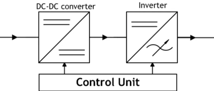
The common arrangement of an VFD, depicted in Figure 1.2, comprises rectification, power factor correction and inversion.
The main reasons that have led to this transform in many of the last generation large ap-pliances are mainly related with speed control, which gets significantly simplified when these structures are used, attaining important gains in terms of energy efficiency. As depicted in Figure 1.3, an air conditioner system controlled by means of a VFD can maintain the compressor running at a constant speed (or close to that). In a traditional system this is not feasible; the compressor can only be turned on or off, which implies higher energy consumption.
A careful analysis of Figure 1.3 allow us to make an important remark: VFDs make use of a DC bus inside the drive. Thus, the long list of DC-compatible loads of our dwellings gets even longer, as VFDs allow the use of DC power supplies. As these structures are starting to be applied
Figure 1.2: Simplified structure of an electronic frequency regulator. Adapted from [4].
Figure 1.3: Behaviour of a traditional air conditioner vs. air conditioner with VFD. Extracted from [5].
by many of the most important manufacturers of household large appliances, it is expected that other companies will follow the same steps. Therefore, a generalization in the use of VFDs in the large appliances of our dwellings is expected.
Nevertheless, more changes are being witnessed in the way our energy is consumed in our dwellings. The electric vehicle (EV), facing a fast expansion phase, is expected to represent a huge amount of energy consumption in our dwellings because of its recharging process. This process requires the connection into a common socket. However, and like any other energy storage system made from batteries or super-capacitors, an AC-DC conversion is required to supply the batteries of the EV [6].
1.1.2
Domestic Microgeneration Evolution
Deep transformations occurred in the type of loads that we possess in our dwellings. Besides that, the importance of each type of load in the overall energy consumption of a dwelling changed significantly (small appliances increased their importance in the overall energy con-sumption of a dwelling and, on the other hand, large appliances reduced their significance). Nevertheless, the changes were not limited to the way energy is consumed in our dwellings. Big changes were also stated in the way energy is produced. An increase in the number of dis-tributed generation systems was stated, encouraged by environmentally friendly policies. Figure 1.4 gives a general view about the growth in the installed capacity related with microgeneration systems in Portugal between 2008 and 2011. It should be noted that a small percentage of the installed power refers to other microgeneration systems that do not belong to domestic systems. These systems make use of some renewable sources of energy and are usually constituted
Fault Tolerant DC-DC Converters 0 10 20 30 40 50 60 70 2008 2009 2010 2011 Po wer ( MW ) Year
Installed power related with microgeneration systems
Figure 1.4: Total installed power related with microgeneration systems. Adapted from [7].
by photovoltaic modules and/or small wind turbines. The majority of these systems operate in DC [8, 9]. Moreover, most of the energy produced by these systems are currently injected into the grid, which implies the use of DC-AC converters to realize the interface between microgen-eration systems and the grid.
1.2
Finding the Best Ways to Save Energy
The energy conversion processes made by means of power electronic converters suffer, in gen-eral, cuts in the conversion efficiency as the number of conversion steps increases. As the converters used for the tasks referred above usually comprises several conversion steps (the most common are transformation, rectification/inversion and power factor correction), they present fairly low efficiencies, as stated in [10].
1.2.1
Alternative Grid Architectures
Taking into account all these evidences (the growth of the DC-compatible home appliances, the increasing number of microgeneration plants and the poor performance of power rectifiers and inverters), it is mandatory to find other options. Reducing the number of power conversion stages would significantly reduce the required equipment, leading to lower power losses in the conversion process. Such reduction could be reached by adopting small-scale DC distribution grids applied at the residential level. This way, microgeneration plants and DC-compatible loads could be connected each other, using DC-DC converters as the interface structure between mi-crogeneration facilities and loads. As DC-DC converters involve a reduced number of components and, hence, of conversion steps, these converters present, generally, higher efficiencies when compared with AC-DC or DC-AC converters. If we consider again the VFD, whose architecture currently implemented in many household appliances is depicted in Figure 1.2, and transpose it to a solution where DC grids are implemented, the result will be similar to that presented in Figure 1.5. As seen in Figure 1.5, the rectification process is eliminated when a DC supply is used, which is why DC-DC converters may present a solution with higher efficiency.
Similarly, we can generalize the DC grid concept to an entire building. Figure 1.6 establishes a comparison between the status quo of the energy distribution system in a dwelling (Figure
Figure 1.5: Simplified structure of an electronic frequency regulator supplied with DC.
1.6(a)) and a feasible alternative (Figure 1.6(b)). It should be mentioned that a DC power distribution system containing an energy storage system, similar to that presented in Figure 1.6(b), may connect the energy storage devices (batteries or super-capacitors) to the DC bus without resorting to DC-DC converters, depending on the system specifications. When those converters are dispensed, the losses related to the power transfer between energy storage devices and DC bus are fairly low (0% to 2% losses). However, slightly higher losses should be expected if power converters are used in the process.
Several case studies proposed alternative embodiments to the conventional power distri-bution system at the residential energy distridistri-bution level, establishing a comparison with the actual systems [12–15]. Despite the small differences between the proposed models, all of them showed that it is possible to significantly reduce the energy losses related to conversion from AC to DC if such variations were implemented. The systems applied in those studies have a high resemblance degree with the one presented in Figure 1.6(b), with the replacement of AC-DC and DC-AC converters for DC-DC converters as a common denominator.
Alongside with this studies, further initiatives are being developed by international institu-tions, namely IEEE. One of them, called “DC in the Home” [16], intends to appoint and quantify the energy losses resulting from the state-of-the-art power electronic converters and, at the same time, establish which steps should be considered in the implementation of this alterna-tive. A similar initiative, called “Indian Low Voltage DC Forum” [17], takes on similar aims. It intends to accomplish real environment tests that prove the effectiveness of these solutions. At the same time, it also aims to contribute on making informed decisions about the most effective way to deploy low an medium DC voltage systems.
DC-DC converters will be, therefore, required in DC grids to provide several DC voltage levels that satisfy the requirements of the different loads. This presents a presage about the relevance that these converters may play in the energy conversion for household systems and many other applications.
Other important measures will be required to enable the full deployment of the solutions proposed above. Besides efficient and reliable DC-DC converters, it is also important to develop several auxiliary systems, as for instance protection systems compatible with DC. Most of the protection technologies currently available for AC systems are not compatible with DC. Circuit breakers and power electronic protection devices are two examples of protection technologies. These protections will be needed for application in sockets, switches, energy storage systems, Power Electronic converters, and so on. Researchers are starting to develop some solutions related to this topic, specially circuit breakers [18, 19], and DC sockets and switches [20–22].
Fault Tolerant DC-DC Converters
(a)
(b)
Figure 1.6: Power distribution system in a dwelling: (a) Typical structure; (b) Proposed structure. Adapted from [11].
1.2.2
Last Generation Semiconductors in the State-of-the-Art Power
Convert-ers
Other ways to reduce the AC-DC energy conversion losses, or vice-versa, could be also used to make a quicker transition to a solution with efficiency improvements.
The developments achieved in the Power Electronics field in the last few years were sig-nificant, with the deployment of faster and more efficient semiconductors, as for instance the Wide Bandgap semiconductors of GaN and SiC. The denomination given to these materials are related to the higher electronic bandgap between electronic levels or, in other words, the gap between the valence band and the conduction band. Table 1.1 compares the bandgap between the most common semiconductor materials [23].
Table 1.1: Semiconductor materials.
Material Bandgap Energy (in eV)
Si 1.1
SiC 3.3
GaN 3.4
The features of these materials can overcome the main constraints of Si devices, being able to block high voltage levels, operate at high-temperature conditions and high switching frequen-cies. These features allow, therefore, the power converters performance enhancement when these devices are used. Further benefits can be attained when using Wide Bandgap devices, as for instance, reduction in the power converter materials (bulky cooling systems can be reduced due to the lower switching losses; passive components can be reduced due to higher switching frequencies) [24].
Both GaN and SiC present high performances, though GaN offers better theoretical results in terms of high-frequency and high-voltage operation. However, better quality substrates are available for SiC devices, putting SiC in a better position to manufacture power switches in the high-voltages segment and GaN in the low/medium-voltages. Nevertheless, plenty of work still needs to be developed to fully exploit the benefits of these materials, starting with improve-ments in the substrates quality and matured manufacturing processes [24].
Thus, the application of the last generation semiconductors in the state-of-the-art power converter topologies (AC-DC and DC-AC) would reduce the losses related to energy conversion processes. However, this solution would not be the most interesting one as it would not reduce significantly the bill of material of those converters and, hence, the potential reduction in the converter losses would not be fully exploited.
1.3
Loads Susceptibility to Voltage/Current Fluctuations
Many of the DC-compatible household appliances, specially electronic loads (e.g. computers, printers, televisions, smartphones, LED lighting, etc.) are very sensitive to voltage and current fluctuations. From the point of view of the solutions proposed in [12–15], where the interface between grid and these loads are performed by means of DC-DC converters, the adoption of low cost DC-DC converters able to ensure high efficiency, high reliability and low output current ripple to such loads is crucial.
im-Fault Tolerant DC-DC Converters
portance. Such levels should remain as high as possible, even if any component of the converter becomes faulty. A fault in a converter component means, in most cases, lower power quality lev-els that endangers the load connected to the converter. Once connected to a faulty converter, those loads experience overheating, leading to their early ageing or, in some cases, to complete stoppage of the load operation, depending on the depth and duration of the fault [25, 26].
A large amount of household appliances use batteries, whereby the same negative effects could be expected in the battery’s lifespan. As show in [27], the ripple of the voltage applied to a battery during the charging process should not surpass 0.5% of the DC voltage, under normal conditions. The same effects can be expected in the converter output capacitor when the current crossing the capacitor present high ripple levels [28].
Interleaved DC-DC converters are one of the topologies that fulfil the above requirements. The input current of the converter is split into n phases, with each phase current shifted by 2π/n radbetween subsequent phases. In fact, great benefits are attained with this approach, namely ripple reduction in both input and output current and lower per phase current rates [29]. Besides that, this is a multi-phase converter, allowing the converter operation continuity, even if one or more power switches stops working (fault isolation remains as a fundamental condition for continued operation).
1.4
Previous Studies in the Domain of DC-DC Converters
1.4.1
Most Common Components Prone to Failures
Power converters, like many other equipment, can suffer from the occurrence of failures. In-side these converters, several components might be the cause of faults. Nevertheless, semi-conductors and capacitors are the most common source of faults in power converters. Within semiconductor faults, that can be classified into open-circuit faults and short-circuit faults, the open-circuit faults are generally caused by gate drivers failures, wire lifting or soldering break [30, 31].
Therefore, the detection of such failures is essential. The adoption of control strategies that reduce the impact of such faults in the load and other converter components is even more important. Some work on short-circuit faults in DC-DC converters have already been made [32–34]. Although detection of such faults can be achieved through software, several protection measures against this kind of failures are already implemented in the state-of-the-art DC-DC converters, namely physical protection devices that isolate the fault in a shorter time when compared with similar protection strategies implemented using software. Short-circuit faults require a fast response time that allows the fault isolation, thus minimizing damages in the converter and/or the load connected to it. Generally, software protection does not achieve the quickness needed to the minimization of adverse impacts of these faults. Additionally, these faults present a big barrier or even inability to the converter operation continuity.
On the other hand, open-circuit faults are not so damaging as short-circuit faults. In the case of the converter under study, the energy supplied to the load is sustained as the rest of the healthy phases keep conducting. Nevertheless, this energy is supplied to the load under worst conditions (more ripple and lower power factor), which is why many of the research effort focuses on open-circuit faults. The current ripple in the input side of the converter also suffers an important growth.
1.4.2
State-of-the-Art on Open-Circuit Fault Detection and Reconfiguration
Several open-circuit fault detection methods applied to different kinds of DC-DC converters have been proposed by several authors. Different strategies were applied to achieve the open-circuit fault detection: use of Kalman filters [35], measurement of the transformer primary voltage and its behaviour analysis [36], comparison of the duty cycle with the inductor current slope [37], analysis of the current waveform and its variation in different points of the converter [33,38–41], capacitors voltage monitoring [42, 43], magnetic near-field waveforms monitoring [44], use of a state estimation approach [45] or the magnetic components voltage waveforms [46]. These works were performed for different topologies of DC-DC converters. Some of them are restricted to specific topologies of DC-DC converters; some fault detection algorithms are just concerned about some operating points of such converters, as for instance converters switching under either zero voltage or zero current conditions or just under discontinuous conduction mode (DCM) or continuous conduction mode (CCM); others have a broad spectrum of action, but are very complicated or have long fault detection times.
Although fault detection assumes a major importance, converter reconfiguration after a fault also plays an important role, as it allows operation continuity with acceptable quality levels. It is relevant to deploy reconfiguration strategies able to maintain the fault-tolerant converter hardware structure as simple as possible, considering a fault-tolerant converter without any additional hardware the most attractive solution. Load and the output capacitor are the most benefited components, as similar levels of pre-fault power quality are achieved, even after the open-circuit fault. Nevertheless, the healthy IGBTs are subjected to slightly higher current ratings and, therefore, higher heating as a consequence of increased conduction losses. For that reason, special careful must be taken when a faulty converter operates at its full load, or close to that operating condition.
To address these concerns, this dissertation applies a fast open-circuit fault detection al-gorithm and reconfiguration strategy after a fault in any of the converter phases. The fault detection algorithm follows the principle used in [41], with the implementation of such princi-ple in multi-phase DC-DC converters. In [33], an identical approach is applied to single-switch DC-DC converters using a state-machine.
After detecting a fault in any of the IGBTs, the PWM generator changes the features of the PWM signals in order to re-organize the converter operation, without any additional hardware devices.
Chapter 2
Converter Operation
This chapter provides detailed information about the operating principles of the converter used in this work. The control strategy applied in the converter is also explained. After that, both normal and faulty operation are compared. Based on this comparison, strategies suitable for fault detection can be discussed.
2.1
Converter Control Strategy
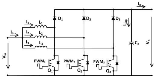
Figure 2.1: Three-phase interleaved DC-DC boost converter.
Figure 2.1 depicts the three-phase interleaved boost converter used for this study. As this converter is composed of three phases, a phase-shift of 2π/3 rad between each phase current is applied to produce a pattern similar to a three-phase current system. Depending on the con-duction pattern of each phase inductor, this converter may operate in three distinct modes: discontinuous conduction mode (DCM), boundary conduction mode (BCM) or continuous conduc-tion mode (CCM). Each operating mode has its advantages and disadvantages. One of the major differences between DCM and CCM is the fact that conduction losses are dominant in DCM, while switching losses are the most important source of losses in a converter operating in CCM. Never-theless, some authors made deeper analysis on the efficiency of these converters. One of those studies presented the pros and cons of both DCM and BCM [47].
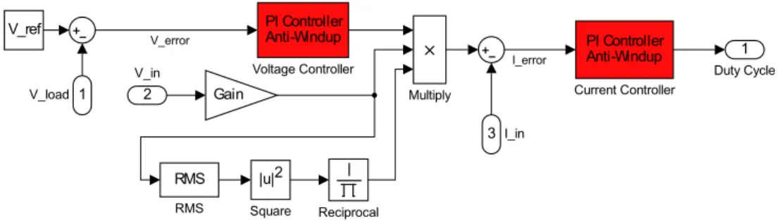
Switched power converters usually require complex control strategies. Several control strate-gies are available, with different complexity degrees. For lower voltage step-up ratios and light-load conditions, a simple voltage controller might be applied to effectively control the converter, with reasonable results. In these conditions, a single PI controller whose input is the output voltage error, given by the difference between Vref and Vo, can perform the task
with success. This is due to the fact that, under these conditions, the converter generally oper-ates in DCM, which allows a stable converter operation, without significant imbalance between converter phases.
Converter operation in CCM brings some problems to the voltage control strategy, causing serious current imbalance between converter phases related to small differences between phys-ical components, especially inductors, and mismatch in the duty cycles applied to each power switch. This instability is harmful for the power switches due to unequal current sharing be-tween converter phases that cause thermal stress to the phase(s) with current surplus. Hence, it is desirable to apply another control strategy able to manage the converter operation with good results in a wider range. An average current control strategy can successfully solve most of these problems. In this strategy, two control loops are used: a voltage regulator and a current regulator. The voltage control loop is the external loop and adjusts the converter output voltage using a PI controller. This regulator uses a small bandwidth to avoid the negative effects of the input ripple in the converter output voltage. The output of this loop, along with the sampled values of the input voltage Vinand the square value of the RMS voltage Vin, are going to define
the value of the reference current Iref. Before using it in the controller, the amplitude of the
input voltage Vin signal is reduced, by applying a reduction factor. This reference signal,
in-troduced in the current control loop, has the same shape and phase of the input voltage signal. This loop, called the inner loop, is responsible for correcting the current error, defined as the difference between the reference current Iref and the effective converter input current Iin.
Besides that, this loop has a wide bandwidth that enables a fast response from this regulator, allowing it to track fast oscillations in the current reference signal [48–50]. This approach is commonly used in converters dedicated to power-factor correction.
However, this work took another approach. Unlike other works that focus the control of interleaved DC-DC converters for power-factor correction effects, this work focuses on appli-cations where the DC-DC converter input is a stabilized DC voltage and, at the same time, uses simple loads to perform the laboratory tests. So, instead of using the original version of Vin,
this signal is filtered to limit the oscillations of Vinseen by the controller, using a discrete low
pass filter for that purpose. Figure 2.2 shows the blocks used in the implementation of such control strategy.
V_ref PI ControllerAnti-Windup
Voltage Controller PI Controller Anti-Windup Current Controller Multiply |u|2 Square Reciprocal Gain RMS RMS 1 V_load 3 I_in 1 Duty Cycle 2 V_in I_error V_error
Figure 2.2: Average current controller used in the interleaved DC-DC boost converter.
This control strategy presents a wide applicability range. It can effectively control the inter-leaved DC-DC boost converter in both DCM and CCM modes. Likewise, it can also control many other switching power converter topologies. Similar strategies based on the same principle have also been developed to overcome some issues that may arise. Interleaved DC-DC converters may show some imbalance between phases, even with this control strategy. To avoid this, all induc-tor currents are compared between them and, in case of imbalance, an adjustment in the duty ratio is introduced [49].
Fault Tolerant DC-DC Converters
2.2
Circuit Behaviour under Normal Operation
The converter input current comprises the sum of each phase current (2.1).
Iin= I1+ I2+ I3 (2.1)
Each converter phase possesses identical components, whereby a balance between phases is expected. However, small differences between phase inductances or parasitic resistances may impair this balance [51]. Therefore, the range of values assumed for each phase current will be similar. With this in mind, and considering the fact that Iin is commonly used for control and
safety purposes, this signal can be one of the best options to monitor an abnormal behaviour of the converter.
Taking into account the identical nature between phases, an analysis will be performed for just one converter phase. When the power switch is conducting, the voltage across the inductor equals the input voltage. On the other hand, the current crossing the switch is equal to the current crossing the inductor. Therefore, the derivative of the inductor current will be given by (2.2).
dIL dt =
Vin
L (2.2)
This means that the slope of the current crossing the inductor is constant and positive, increasing linearly while the switch is on.
Meanwhile, when the switch is off, no current flows through it. The voltage across the inductor, given by the difference between the source and load voltages, is negative as the load voltage is higher than the source voltage. Therefore, the derivative of the current flowing through the inductor is given by (2.3).
dIL dt =
Vin− Vout
L (2.3)
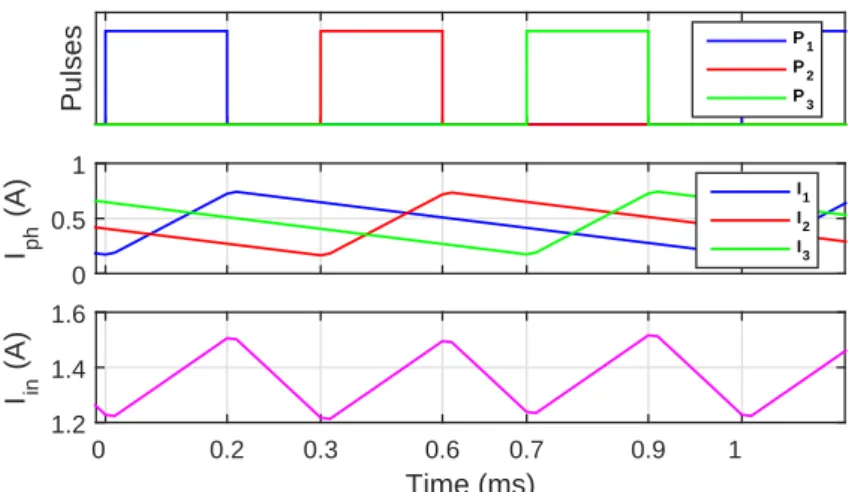
Hence, the current crossing the inductor during this time period will decrease linearly after the switch turn-off, possibly reaching zero, depending on the converter operating mode. The behaviour of these variables is depicted in Figure 2.3.
Pulses P1 P2 P3 I ph (A) 0 0.5 1 I 1 I2 I 3 Time (ms) 0 0.2 0.3 0.6 0.7 0.9 1 I in (A) 1.2 1.4 1.6
2.3
Circuit Behaviour under Faulty Operation
After an open-circuit fault in a power switch, no current will flow through it, precluding any energy flow across the phase associated with that IGBT. Thus, only (2.3) will be verified, meaning that after a fault, the phase current will decrease linearly, reaching zero phase current soon. The frequency of the input current ripple decreases, resulting in an increase in the current ripple in both the input and output of the converter. Figure 2.4 shows a switching pattern with a power switch open-circuit fault in phase 1 at t = 0.1 ms.
Pulses P1 P2 P3 I ph (A) 0 0.5 1 I1 I2 I3 Time (ms) 0 0.2 0.3 0.6 0.7 0.9 1 I in (A) 0.5 1 1.5
Figure 2.4: Operation of the converter after an open-circuit fault in the power switch of phase 1 at
t = 0.1 ms.
As expected, the phase current starts to decrease linearly until reaching zero. This behaviour is usually reflected in the waveform of Iin. When it happens, Iin decreases until the switch
related to the next phase starts conducting. However, it does not occur every time, because the relation between the duty ratio D of the PWM applied to the IGBTs and converter operation mode might determine the maintenance of the increasing trend of Iin. Such behaviour occurs
when D > 2/3 or 1/3 < D < 2/3 and the converter operates at DCM.
The duty ratio D, along with DM, are responsible to determine the converter step-up ratio. DM can be defined as time wherein the phase current is different from zero. In both BCM and CCM DM is equal to 1, because the phase current never reaches zero. Hence, the converter
voltage gain is given by (2.4) [38].
Vout Vin =
DM
DM − D (2.4)
Therefore, the control structure comprising fault diagnosis and converter reconfiguration has to be applied. The main functions of each block will be detailed in the next chapters.
Chapter 3
Fault Diagnosis
As mentioned in Chapter 2, the converter input current Iincontains important information that
can be used for fault detection purposes. Fault detection can be achieved by acquiring and comparing the values of Iinin different and well-defined moments. The pulses used to trigger
each power switch are easily available from the control structure, making them a good choice to define those moments. Using Iinas the control variable and the PWM signals together, a trivial
solution consisting on the comparison of Iinin the rising edge of the PWM signal related to that
phase, and the corresponding falling edge can be used in this converter, similarly to what is suggested in [41].
An identical approach is used in [33], where the inductor current slope sign is used to detect a fault (open-circuit or short-circuit faults). As depicted in Figure 2.3, Iin increases after the
switch turn-on, and will remain increasing until the next falling edge, that can belong to any control signal. To take this into account, the values of Iinin the rising edge will be compared with
the values in the first falling edge of any of the command signals, making this verification step independent of the duty cycle D. The presence of an open-circuit fault can be easily analysed by subtracting the last value of Iinsaved in the sample and hold block with the last value from
the stack: if the difference is positive (Iinincreases in the time period under analysis), it means
that the power switch associated with that phase is healthy; otherwise Iin decreases and an
open-circuit fault has occurred in the power switch of that phase. A similar approach can be used to detect also short-circuit faults, taking into account different time intervals. Compared with other open-circuit fault detection algorithms, this reduces the fault detection time. This reduction is especially significant when the converter operates with 1/3 < D < 2/3. On the other hand, this fault detection algorithm is unable to detect faults when the duty cycle D > 2/3 or the duty cycle D is 1/3 < D < 2/3 and the converter operates at DCM. Within the subject of this work, these operating points are not applied because of their low interest in terms of converter efficiency.
To improve the fault detection effectiveness, a first-order high-pass filter is added to process the Iin signal. With this filter, fault detection capability gets enhanced, with improvements
on fault detection under harsh converter operation, as for instance load transients. A gain is introduced in the filtered signal to amplify it and give a cleaner view of the signal variations. The basic structure of the fault detection block is presented in Figure 3.1.
The main blocks composing this unit are the stack, the sample and hold, the high-pass filter, the S-R flip-flop and the edge detectors. The working principle is simple: when a rising edge is detected in the PWM signal, the filtered signal of Iin is pushed into the stack block. When
a falling edge in any of the PWM signals is detected, the filtered signal of Iinis stored in the
sample and hold block, being instantaneously sent to the block output. At the same time, the last value in the stack is popped, so the values of Iinrelated to the same switching period can
be correctly compared. The S-R flip-flop ensures that only falling edges subsequent to the rising edge in analysis are taken into account.
With this configuration, the block compares the values of Iin in the rising edge of the PWM
OR S R Q !Q S-R Flip-Flop Z-1 1-Sample Delay High-Pass Filter 200 Gain Z-1 1-Sample Memory 1 Control pulses 2 Current 1 Phase 1 fault <= 0 Compare To Zero In S/H Stack In Push Pop Rst Out Full Full Full
Figure 3.1: Basic structure of the fault detection block.
detection for a wide range of duty cycle values. Figure 3.2 illustrates the sampling moments of
Iinfor different values of D.
However, some issues may arise when this sampling strategy is used for the converter oper-ation with values of D near or equal to 1/3 and 2/3. For such duty cycle values, the falling and rising edges of the PWM signals are very close to one another’s and the power switches change of state almost simultaneously. In these conditions, the ripple of Iinis minimum, making the fault
detection process much more complex. In addition, the non-ideal behaviour of the converter components, verified in any practical implementation, also impacts the fault detection. Under these circumstances, Iinmaintains its descending trend for a few moments after the rising edge
of the PWM signal that triggers the IGBT related to the phase under analysis. To overcome this issue, a small delay is applied to the signal that triggers the Push into stack when two edges are close to one another. The delay depends on the switching frequency fs, duty cycle D and
sampling time of the controller Ts. This time delay increases as the time distance between
both shortens. The fault detection block requires a few more components to correctly apply the delay, when needed. Hence, a delay block and a function block, responsible to create the expression that computes the number of samples of the delay, are added. Figure 3.3 displays the fault detection block with capability to change the moment for pushing the value of Iininto
the stack when D approaches 1/3.
When D approaches 1/3, the stack block saves the processed values of Iinin two moments:
the first occurs in the rising edge of the PWM signal; the second appears after the PWM rising edge and represents a delayed version of the last verified falling edge. Figure 3.4 shows an example where D is almost 1/3. There, two pulses are shown, representing the moments when
Iin signal is pushed into the stack. In this case, only the second value of the sampled signal will be used for comparison effects, leaving any other data in the stack until its deletion. The second pulse intends to eliminate the false fault detection phenomena arising from non-ideal behaviour of the converter, that is not presented in Figure 3.4.
The fault detection process explained above applies for one converter phase. Some resources used for this purpose have to be replicated in order to have fault detection in all three phases; blocks with the same results are shared between all converter phases.
Fault Tolerant DC-DC Converters
P
1P
2P
3I
ph(A)
0 0.5 1 I1 I2 I3I
in(A)
1.4 1.6 1.8SW1
onTime (ms)
0 0.3 0.4 0.6 0.7 0.9 1SW1
off (a)P
1P
2P
3I
ph(A)
0 1 2 I1 I2 I3I
in(A)
2 2.5 3SW1
onTime (ms)
0 0.2 0.3 0.5 0.7 0.8 1 1.2SW3
off (b)Figure 3.2: PWM pulses, Phase currents, Converter input current, Push into stack and Pop from stack commands for: (a) D < 1/3; (b) 1/3 < D < 2/3.
OR S R Q !Q S-R Flip-Flop Z-1 1-Sample Delay High-Pass Filter 200 Gain Z-1 1-Sample Memory <= 0 Compare To Zero
f(u)
Fcn d u Z-d Delay OR AND Saturation OR OR NAND 1 Control pulses 2 Current 3 Input current 4 Duty Cycle 1 Phase 1 fault In S/H Stack In Push Pop Rst Out Full Full FullFigure 3.3: Fault detection block with delay capability. The components added to the block are highlighted in red.
P
1P
3I
in(A)
1.6 1.8 2Time (ms)
1.2 1.3Push
Chapter 4
Converter Reconfiguration After an Open-Circuit
Fault
As stated in Chapter 1, it is essential to maintain the good operation of a DC-DC converter, even after an open-circuit fault. It was also verified that a converter whose power switches present open-circuit faults can still deliver power to the load, but under degraded conditions. The most visible effects are the higher fluctuations in the input current Iinand output capacitor current ICap. Higher current variations in this capacitor are experienced to compensate the loss of one
converter phase. As a result, the converter capacitor will be highly stressed, with its possible loss. Remedial actions to reduce the impact of open-circuit faults are, therefore, mandatory.
In the reconfiguration strategy used in [52], with other authors working on multi-phase DC-DC converters suggesting the use of such strategy [34, 37, 38], the converter operation is adjusted according to load requirements or in case of power switches failures. After an open-circuit fault in one or more power switches, the PWM signals phase-shift are adjusted according to the number of healthy phases. In the case of the three-phase interleaved boost converter, the phase-shift between PWM signals associated with healthy phases would be changed from 2π/3 rad to
π radafter an open-circuit fault; the principle is to change the control strategy from a three-phase converter to a two-three-phase converter while the converter is online. The same principle is applied in this work for the converter reconfiguration. This action reduces, in general, the current ripple after a fault, but does not allow the converter to reach the level of ripple verified in the original state of the converter. Therefore, additional actions can be taken to reduce the ripple even more.
The current variation on each converter phase, consisting on the difference between the peak values of the waveform, can be obtained using (4.1) [38]:
IM =
Vin× D × T
L =
Vin× D
fs× L (4.1)
From (4.1), it can be easily deduced that the phase current ripple depends on the input voltage Vin, duty cycle D, switching frequency fsand phase inductance L. After an open-circuit
fault, Iinripple frequency decreases from 3fsto fs, resulting in increased current oscillation,
in accordance to (4.1). All these parameters, except D and fs, are fixed or cannot be changed
to maintain specific ripple levels. On the other hand, D is used to define the converter step-up ratio, making its use for ripple reduction effects infeasible. Hence, switching frequency fscan
be used, under fault conditions, to minimize current ripple in both the input and output of the converter. Some authors have already developed work related with frequency modulation in DC-DC converters drivers [53–55], but not with fault tolerance purposes. Others have worked with frequency modulation for fault tolerant converters, but for different topologies [37], applying just this reconfiguration strategy. Thus, a control consisting on a combination of adaptive phase-shift and frequency modulation can perform the reconfiguration task with good results.
Here, the idea is to adapt the phase-shift between PWM signals and, at the same time, increase the switching frequency fs after a fault. To implement such strategy, the block from
Figure 4.1 is used. The most important components are the PWM generator and the phase-shift corrector. Frequency Duty cycle Phase 2 f actor Phase 3 f actor PWM1 PWM2 PWM3 PWM generator Fpwm Base frequency Fpwm Gain Phase 1 f ault Phase 2 f ault Phase 3 f ault Phase 2 f actor Phase 3 f actor Phase correction 1 Phase 1 fault 2 Phase 2 fault 3 Phase 3 fault 4 Duty Cycle 1 Carrier Frequency 2 PWM1 3 PWM2 4 PWM3
Figure 4.1: Reconfiguration block.
4.1
Phase Correction Component
The phase-shift corrector contains a combinational logic circuit. In the simulation environment, each signal introduced in this component is delayed by one sampling period to avoid algebraic loop errors. According to the information given to this block about the presence and location of faulty phases, the outputs will change the values sent to the PWM generator. Table 4.1 summarizes the possible fault combinations and the corresponding phase-shift between PWM signals. The applied shift takes the PWM signal for phase 1 as reference. In this table, ’-’ denote the do not care state. In other words, the phase-shift may remain unchanged if a transition to that state is verified. For the sake of simplicity, the block was configured with default values (a phase-shift of 1/3T for phase 2 and a phase-shift of 2/3T for phase 3, where T denotes the PWM signals period).
Table 4.1: Possible fault combinations and their corresponding phase-shifts in the time domain.
States Phase shift (x× T )
Ph.1 fault Ph.2 fault Ph.3 fault Ph.2 shift Ph.3 shift
0 0 0 1/3 2/3 0 0 1 1/2 2/3 0 1 0 1/3 1/2 0 1 1 - -1 0 0 1/3 5/6 1 0 1 - -1 1 0 - -1 1 1 -
-Generally speaking, this component applies a phase-shift of 1/2T to the PWM signal related to the second healthy power switch. To exemplify, let us consider the following example: after an open-circuit fault in Q1, Q2 and Q3 hold their operation; thus, a phase-shift of 1/2T between PWM2 and PWM3 has to be applied. To avoid using three output variables in this block, the phase-shift of PWM2 remains unchanged, while PWM3 phase-shift is increased from 2/3T to 5/6T. Figure 4.2 depicts such variation in the PWM signals after the occurrence of an
open-Fault Tolerant DC-DC Converters
circuit fault. Signals with same colours refer to the same converter phase. PWM1 is disabled after the fault and, as expected, the other two PWM signals are reconfigured instantaneously.
4.2
PWM Generation Component
This component generates PWM signals for all the three converter IGBTs. To ensure the capabil-ities of fault tolerance, carrier frequency and phase-shift are introduced as inputs in the block to allow these reconfiguration capabilities. PWM signals are produced by a triangular carrier, generated with the aid of two discrete integrators and one look-up table.
The carrier frequency assumes predefined discrete values. Under normal operation condi-tions, switching frequency fs remains unchanged along the converter operation and it is equal
to the frequency previously defined for the converter operation. After an open-circuit fault, fs
is increased to the double of the original fsvalue. In the case of a second open-circuit fault, fs
is subjected to a new increase. In the example illustrated in Figure 4.2, the increase of fsafter
fault detection is notorious.
Ph.2 shift 0 0.5 Ph.3 shift 0.6 0.8 1 Time (ms) 0 3 6 Pulses P 1 P 2 P 3
Figure 4.2: PWM reconfiguration after an open-circuit fault in Q1 at t = 3.1 ms.
It should be noted that the use of the reconfiguration strategy, just like in any other converter working under faulty conditions, leads to higher current rates in the healthy power switches that remain operating. This stresses those switches and leads to higher conduction and switching losses, with possible overheating. Converter operation with full load conditions should be, therefore, avoided under these circumstances. Besides that, fsmust be kept inside reasonable
Chapter 5
Simulation Results
The solutions proposed in the previous chapters were simulated using MATLAB/Simulink to con-firm their effectiveness. The elements and parameters used for simulation purposes were ap-proached as much as possible to the equipment used for experimental purposes.
Figure 5.1 reflects the full system comprising fault detection and reconfiguration.
Gate IGBT3 Gate IGBT2 Gate IGBT1 Uin+ Uin-Uout+
Uout-Interleaved boost converter
Phase 1 f ault Phase 2 f ault Phase 3 f ault Duty Cycle Carrier Frequency Pulse1 Pulse2 Pulse3 PWM Generator + C + Load Current Duty Cycle Carrier f requency Control pulses
Phase 1 f ault (Y/N)
Phase 2 f ault (Y/N)
Phase 3 f ault (Y/N)
Fault Location
1
V_load
V_ref PI ControllerAnti-Windup
Voltage Controller PI Controller Anti-Windup Current Controller Gain 3I_in Multiply |u|2 Square Reciprocal RMS RMS Rate Limiter A B C + -Rectifier N A B C Three-Phase Voltage Source + C1 2 V_in num(z) den(z) V_out Filter num(z) den(z) V_in Filter
Figure 5.1: Overview of the entire system.
The main parameters used in this simulation are summarized in Tables A.1 to A.5 from Ap-pendix A. Several levels were considered for the converter output voltage Vo, in order to address
a wide range of duty cycle D values. A constant resistance load is considered in the tests. Figures 5.2, 5.3 and 5.4 establish a comparison between the most important converter vari-ables for three different circumstances: in Figure 5.2, no reconfiguration is used after a failure in one of the converter phases; in Figure 5.3, partial reconfiguration is used after a failure, by correcting the phase-shift between healthy phases; and in Figure 5.4, phase-shift correction and frequency modulation are applied after a failure, to get full reconfiguration in the converter. The simulation results presented in these figures were performed for a converter output voltage of 48 V .
A comparison study between Figure 5.2 and Figure 5.3 allow us to take some conclusions. A decrease in the ripple has occurred in many of the converter electrical parameters, especially in Iin. Despite the fact that phase-shift plays an important role in ripple cancellation after an
open-circuit fault, further improvements in the limitation of ripple are attained after combining the increase of fswith phase-shift correction. Figure 5.4 proves such statement. Under similar
circumstances, like those verified in Figures 5.3 and 5.4, the ripple can be reduced with the increase of the fs to the double of its initial value. An important reduction in the ripple of
ICapis also verified when the reconfiguration strategies are applied. It is even more important the fact that, after applying full reconfiguration in the converter, it is possible to maintain the levels of ripple in ICapassociated with healthy operation (see Figure 5.4(g)). Besides that, the
transient of Iin that remains high (see Figure 5.3(a)) is reduced when full reconfiguration is
applied (see Figure 5.4(a)). The same conclusions can be taken from Figure 5.5, where Iin is
depicted with more detail.
The simulation results presented here focused on the converter operation for constant re-sistive loads. Nevertheless, load fluctuations are also important events that must be taken into account. Therefore, such events should be simulated to attest that false fault detections do not occur. Figure 5.6 depicts the transient verified when one of the two loads initially connected to the converter are unplugged (for t = 0.5 s). Both loads have the same resistance and, hence,
Iodecreases to half of its initial value. This transient does not generate false fault detection in
Fault Tolerant DC-DC Converters Time (s) 0 0.05 0.1 0.15 0.2 0.25 0.3 0.35 0.4 0.45 0.5 Iin (A) 0 5 (a) Time (s) 0 0.05 0.1 0.15 0.2 0.25 0.3 0.35 0.4 0.45 0.5 Vin av (V) 21 21.5 22 (b) Time (s) 0 0.05 0.1 0.15 0.2 0.25 0.3 0.35 0.4 0.45 0.5 Pin (W) 0 50 100 150 (c) Time (s) 0 0.05 0.1 0.15 0.2 0.25 0.3 0.35 0.4 0.45 0.5 I out (A) 1.5 1.6 1.7 (d) Time (s) 0 0.05 0.1 0.15 0.2 0.25 0.3 0.35 0.4 0.45 0.5 V out (V) 46 48 50 (e) Time (s) 0 0.05 0.1 0.15 0.2 0.25 0.3 0.35 0.4 0.45 0.5 Pout (W) 60 80 100 (f) Time (s) 0 0.05 0.1 0.15 0.2 0.25 0.3 0.35 0.4 0.45 0.5 I Cap (A) -2 0 2 (g) Time (s) 0 0.05 0.1 0.15 0.2 0.25 0.3 0.35 0.4 0.45 0.5 Ph.1 fault 0 0.5 1 (h)
Figure 5.2: Converter variables evolution when an open-circuit fault occurs in one of the converter IGBTs (at t = 0.25 s) and no reconfiguration actions are taken: (a) Iin; (b) Vinav; (c) Pin; (d) Iout; (e) Vout; (f)
Pout; (g) ICap; (h) Phase 1 fault detection flag. Switching frequency fsis equal to 1 kHz and remains
Time (s) 0 0.05 0.1 0.15 0.2 0.25 0.3 0.35 0.4 0.45 0.5 Iin (A) 0 5 (a) Time (s) 0 0.05 0.1 0.15 0.2 0.25 0.3 0.35 0.4 0.45 0.5 Vin av (V) 21 21.5 22 (b) Time (s) 0 0.05 0.1 0.15 0.2 0.25 0.3 0.35 0.4 0.45 0.5 Pin (W) 0 50 100 150 (c) Time (s) 0 0.05 0.1 0.15 0.2 0.25 0.3 0.35 0.4 0.45 0.5 Iout (A) 1.5 1.6 1.7 (d) Time (s) 0 0.05 0.1 0.15 0.2 0.25 0.3 0.35 0.4 0.45 0.5 Vout (V) 46 48 50 (e) Time (s) 0 0.05 0.1 0.15 0.2 0.25 0.3 0.35 0.4 0.45 0.5 Pout (W) 60 80 100 (f) Time (s) 0 0.05 0.1 0.15 0.2 0.25 0.3 0.35 0.4 0.45 0.5 ICap (A) -2 0 2 (g) Time (s) 0 0.05 0.1 0.15 0.2 0.25 0.3 0.35 0.4 0.45 0.5 Ph.1 fault 0 0.5 1 (h)
Figure 5.3: Converter variables evolution when an open-circuit fault occurs in one of the converter IGBTs (at t = 0.25 s) and partial reconfiguration actions are taken (only phase-shift is corrected): (a) Iin; (b) Vinav; (c) Pin; (d) Iout; (e) Vout; (f) Pout; (g) ICap; (h) Phase 1 fault detection flag. Switching frequency
Fault Tolerant DC-DC Converters Time (s) 0 0.05 0.1 0.15 0.2 0.25 0.3 0.35 0.4 0.45 0.5 Iin (A) 0 5 (a) Time (s) 0 0.05 0.1 0.15 0.2 0.25 0.3 0.35 0.4 0.45 0.5 Vin av (V) 21 21.5 22 (b) Time (s) 0 0.05 0.1 0.15 0.2 0.25 0.3 0.35 0.4 0.45 0.5 Pin (W) 0 50 100 150 (c) Time (s) 0 0.05 0.1 0.15 0.2 0.25 0.3 0.35 0.4 0.45 0.5 I out (A) 1.5 1.6 1.7 (d) Time (s) 0 0.05 0.1 0.15 0.2 0.25 0.3 0.35 0.4 0.45 0.5 V out (V) 46 48 50 (e) Time (s) 0 0.05 0.1 0.15 0.2 0.25 0.3 0.35 0.4 0.45 0.5 Pout (W) 60 80 100 (f) Time (s) 0 0.05 0.1 0.15 0.2 0.25 0.3 0.35 0.4 0.45 0.5 I Cap (A) -2 0 2 (g) Time (s) 0 0.05 0.1 0.15 0.2 0.25 0.3 0.35 0.4 0.45 0.5 Ph.1 fault 0 0.5 1 (h)
Figure 5.4: Converter variables evolution when an open-circuit fault occurs in one of the converter IGBTs (at t = 0.25 s) and full reconfiguration actions are considered: (a) Iin; (b) Vin; (c) Pin; (d) Iout; (e) Vout;
(f) Pout;(g) ICap; (h) Phase 1 fault detection flag. Switching frequency fsincreases from 1 kHz to 2 kHz
Time (s) 0.235 0.24 0.245 0.25 0.255 0.26 0.265 I in (A) 2 3 4 5 (a) Time (s) 0.235 0.24 0.245 0.25 0.255 0.26 0.265 I in (A) 2 3 4 5 (b) Time (s) 0.235 0.24 0.245 0.25 0.255 0.26 0.265 I in (A) 2 3 4 5 (c)
Figure 5.5: Zoom of Iin: (a) no reconfiguration strategy is applied to the converter after fault; (b) partial
reconfiguration (phase-shift correction) is applied to the converter after fault; (c) full reconfiguration is applied to the converter after a fault detection.
I (A) in V (V) o I (A) o Ph.1 fault Ph.2 fault Time (s) 0 0.1 0.2 0.3 0.4 0.5 0.6 0.7 0.8 0.9 1 Ph.3 fault
Figure 5.6: Behaviour of the converter most important electrical parameters after a step variation in the load connected to the converter.
![Figure 1.1: Average residential electricity consumption by end-use in Europe - 27. Adapted from [2].](https://thumb-eu.123doks.com/thumbv2/123dok_br/18656145.912799/20.892.162.681.690.1115/figure-average-residential-electricity-consumption-end-europe-adapted.webp)
![Figure 1.3: Behaviour of a traditional air conditioner vs. air conditioner with VFD. Extracted from [5].](https://thumb-eu.123doks.com/thumbv2/123dok_br/18656145.912799/22.892.211.637.335.577/figure-behaviour-traditional-air-conditioner-conditioner-vfd-extracted.webp)
![Figure 1.4: Total installed power related with microgeneration systems. Adapted from [7].](https://thumb-eu.123doks.com/thumbv2/123dok_br/18656145.912799/23.892.160.768.113.368/figure-total-installed-power-related-microgeneration-systems-adapted.webp)