Microstrip Antenna on a High Dielectric Constant Substrate:
BaTiO
3
(BTO)-CaCu
3
Ti
4
O
12
(CCTO) Composite Screen-Printed
Thick Films
P.B.A. FECHINE,1 A. TA´ VORA,2 L.C. KRETLY,2 A.F.L. ALMEIDA,1 M.R.P. SANTOS,3 F.N.A. FREIRE,1 and A.S.B. SOMBRA3 , 4
1.—Departamento de Quimica Orgaˆnica e Inorgaˆnica-UFC-Universidade Federal do Ceara´ Caixa Postal 12200, CEP 60455-760, Fortaleza, Ceara´, Brazil. 2.—Departamento de Microondas e O´ ptica (DMO), Faculdade de Engenharia Ele´trica e Computacxa˜o (FEEC), UNICAMP CEP 13083-970-Campinas, Sa˜o Pavlo, Brazil. 3.—Laborato´rio de Telecomunicacxo˜es e Cieˆncia e Engenharia dos Materiais (LOCEM) Departamento de Fı´sica, Universidade Federal do Ceara´ Caixa Postal 6030, CEP 60455-760, Fortaleza, Ceara´, Brazil. 4.—E-mail: sombra@fisica.ufc.br
The performance of microstrip antennas using composite thick films of (BTO-BaTiO3) and CCTO (CaCu3Ti4O12) as a substrate were studied. The dielectric permittivity and loss of (BTO)x-(CCTO)1 xthick films with x50, 0.2, 0.5, 0.8, 0.9, and 1 were examined. These films were prepared in two-layer geometry using the screen-printing technique on Al2O3substrates. Mechanical alloying followed by the solid-state procedure was successfully employed to produce powders of CCTO (CaCu3Ti4O12) used in the films. We also studied the films dielectric permittivity (K) and loss (D) in the medium-frequency (MF) range (100 Hz to 1 MHz). The performance of a planar microstrip antenna that uses the (BTO)x:(CCTO)1 xthick films as a substrate of high K was also examined in the microwave range of frequencies. From the analysis of the antenna operation of the samples, one can conclude that the higher values of K in the range of 2.5–3.3 GHz antennas is presented by the BTO substrates. For the BTO film, the K value is;66 (2.6 GHz) and decreases to 34 for the CCTO film (3 GHz). For the BTO and CCTO films, the antenna bandwidths (BW) are ;50% and;38%, respectively. The higher bandwidth presented by the BTO compared to the CCTO is certainly associated with the higher loss presented by the BTO phase, which is a ferroelectric phase. Therefore, these measure-ments confirm the potential use of such materials for small microwave planar antennas, where the miniaturization of the devices is crucial.
Key words:Antennas, high-K materials, dielectric
INTRODUCTION
Thin films ,1 mm have been extensively investi-gated due to their potential applications in micro-electronics and micromechanics. However, less attention has been directed to processing of thicker films. A reasonable number of applications require films of several microns to several tens of microns. Whereas ferroelectric thin films methods have their specific features, ferroelectric thick films processing is closer to that of the bulk ceramics, including pow-der synthesis, powpow-der processing, coating, and sin-tering. Coating is obtained by screen printing, a well-developed processing step in thick-film technology.
Ferroelectric thick films have applications in pyro-electric sensors,1,2gravimetric sensors,3micropumps,4 pressure sensors,5 and surface acoustic wave sensor (SAW)6 devices. Properties obtained are poorer com-pared to the bulk ceramics due to the addition of low-temperature sintering aids and/or high porosity.
Most multichip modules (MCMs) fabricated today require decoupling capacitors to suppress the power-distribution noise.7,8 These surface mount capacitors are large in size, occupy space, and have large parasitic capacitance. Materials with relative dielectric constant (K) in the range of 25–170 are required for advanced decoupling capacitors.
In this paper, we study a composite thick film with two different phases. The first phase is ce-ramic barium titanate (BaTiO3-BTO), a well-known (Received January 24, 2006; accepted April 28, 2006)
ferroelectric material, which has a high dielectric constant (K) of ;6,000 at a fine grain size of ;1
mm, and of 1,500–2,000 at a coarse grain size.9,10 The dielectric constant of BTO at the Curie temper-ature of 120°C can reach a peak value as high as 10,000, but decreases as the temperature decreases. Chemical additives or so called shifters have been applied to BTO to move the Curie peak value toward room temperature to improve the dielectric con-stant, and to smooth the Curie peak to obtain a lower temperature coefficient of the K value.
Dielectric properties of BTO ceramics are highly dependent upon the grain size, phase content of the ceramic body, and type of dopants used. For BTO powder, its behavior is also related to the particle size, phase content, and the dopants added. Cubic BTO (c-BTO) powder transforms to the tetragonal phase (t-BTO) if its size is .30 nm.11 Powder with particle sizes 40–80 nm contains a single domain. Crystallites.80 nm will be multidomain t-BTO.12 The increase of the dielectric constant may be caused by a combination of the domain size and the stress effect.13 It is also known that the width of ferroelectric 90° domains decreases proportional to the square root of the grain diameter for grains ,10 mm.13 Removal of grain boundaries, i.e., elimi-nation of constrained forces from neighboring grains and a drop in domain density as the particle size decreases, may reduce the DC of the BTO powders. With increasing particle size, unsintered powder eventually becomes a ceramic-like body and ac-quires properties similar to ceramics.14 Therefore, ceramics and powders of BTO can show a different dielectric behavior, depending on the particle size.
The second crystalline phase will be in the form of CaCu3Ti4O12 (CCTO).15–17 For this material, high dielectric constants have been found showing a dielectric constant at 1 kHz of;10,000 that is nearly constant from room temperature to 300°C. Oxides with the perovskite structure are well stabilized by their high dielectric constants (K), which lead this class of materials to be used in a large number of technological applications.15However, this behavior is generally associated with ferroelectric or relaxor properties. In these cases, the highest value of K is obtained during a phase transition (as a function of temperature) presented by the material.
Existence of the transition temperature event is generally a problem with respect to the applications of these materials. The reported results for CCTO shows that the K is high but with small dependence on the temperature.16Such material is very promis-ing for capacitor applications and certainly for microelectronics and microwave devices (mobile cel-lular phones, for example), where device miniatur-ization is important.
Use of high K ceramics make possible a noticeable miniaturization of passive microwave devices. Their size can typically be reduced, compared with classi-cal resonators and filters, by a factor of ‘‘ ffiffiffiffi
K
p
’’ (rela-tive dielectric constant). The structure of CCTO was previously determined from neutron powder
diffrac-tion data.17 It belongs to the space group Im3 (No. 204).17Recently, we proposed the use of mechanical alloying to produce CCTO.18 Mechanical alloying has proved to be a powerful technique to obtain any quantity of powder with a controlled micro-structure.19In addition, a polymeric citrate precur-sor route was used to produce CCTO.20 A dielectric constant of 3,000 and loss of ;0.3–0.35 at 1 kHz were observed.
In a recent paper, we reported on the operation of these films as planar microwave antennas. Re-cently, we also reported on the use of the CaCu 3-Ti4O12 (CCTO)21 and BaTiO3 (BTO)-CaCu3Ti4O12 (CCTO)22 substrates for microwave devices and antennas and BaTiO3(BTO)-CaCu3Ti4O12(CCTO) composite thick films for high dielectric constant devices in the medium-frequency (MF) range.23 The performance of a planar microstrip antenna that uses the (BTO)x-(CCTO)1 x thick films as a high-K substrate was examined. These measure-ments confirm the potential use of such materials for small high dielectric planar antennas (HDA).
EXPERIMENTAL METHODS
CCTO Crystalline Powder
Commercial oxides Ca(OH)2(Vetec, Rio de Janiero, Brazil, 97% with 3% of CaCO3), titanium oxide (TiO2) (Aldrich, 99%), and CuO (Aldrich, 99%) were used in the CCTO preparation. The material was ground on a Fritsch Pulverisette 6 planetary mill with the proportionality of Ca(OH)2-3CuO-4TiO2. Milling was performed in sealed stainless steel vials and balls under air. Mechanical alloying was per-formed for 30 min. of milling. In this case, the mill-ing was used only to give a good homogeneity of the powder. However, we already showed in the litera-ture that, for 100 h of milling, complete production of CCTO is possible.18The reaction occurring during milling can be summarized as:
CaðOHÞ213CuO14TiO2
/
ImpactCaCu3Ti4O121H2O
The compounds were also prepared by the conven-tional powder-sintering technique using the same starting materials. The ceramic was submitted to calcination and sintering in air in the range of 900–1,100°C for 12–24 h.17
BTO Powder Preparation
The BTO powder used was a commercial product (BaTiO3-Aldrich). This ceramic is also called BTO (commercial).
Paste Preparation
The paste was prepared from the suspension of organic material (resin, organic solvent, and some additive to improve rheological behavior of the paste) and powders (BTO and CCTO). For better
adhesion between paste and substrate (Al2O3), a low-temperature melting material in powder form (flux material) was added.
Substrates and Electrodes
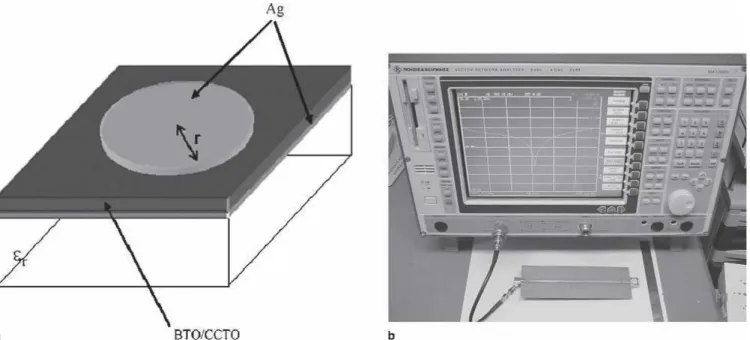
The alumina substrates used, squares of dimen-sions 1.26 cm31.26 cm and thickness 4.8 mm, were commercial products (Engecer, Sa˜o Carlos, Brazil). The electrode material (Ag) was produced by the screen-printing technique (Joint Metal-PC200; Engecer, Sa˜o Carlos, Brazil) in the geometry described in Fig. 5a (thickness ;50 mm). The top electrode is circular with r 5 L/2 (see Fig. 5a and Table II). The bottom electrode was present in the area of the alumina substrate.
Preparation of the Films
The bottom electrodes (Ag) were screen printed on the Al2O3substrate and fired at 850°C for 1 h. On the fired electrode, a first layer was screen printed and sintered for 1 h. After firing the dielectric layer, the upper electrode (Ag) was deposited and then dried and fired at the same temperature-time regime as for the bottom electrode. The obtained films usually had thickness ranging from 140 mm to 190 mm, depending on the number of layers. All the films used in these measurements were composed of two layers. For this paper, we used six types of films: (BTO)x:(CCTO)1 x, where x 5 0, 0.2, 0.5, 0.8, 0.9, and 1. The nomenclature used in this paper is as fol-lows: CCTO, (BTO)0.2:(CCTO)0.8, (BTO)0.5:(CCTO)0.5, (BTO)0.8:(CCTO)0.2, (BTO)0.9:(CCTO)0.1, and BTO, respectively (percentages are given in wt.%).
The film was subjected to the following firing process: 100°C for 1 h1 400°C for 1 h1 900°C for 1 h (first layer) and 100°C for 1 h1400°C for 1 h1 900°C for 4 h (second layer).
X-ray Diffraction
The x-ray diffraction (XRD) patterns were done using a Siemens (Germany) D5000 equipment with Cu Karadiation in Bragg-Brentano geometry at room
temperature (300 K) by step scanning using pow-dered samples. We used 5 sec for each step of count-ing time, with a Cu Katube at 40 kV and 25 mA.
XRD patterns were also obtained at room temper-ature (300 K) by step scanning using the films.
Dielectric Measurements
The dielectric measurements were obtained from a HP 4291 Material Impedance Analyzer (Hewlett-Packard, New York) in conjunction with a HP 4194 Impedance Analyzer, which jointly cover the region from 100 Hz to 1.8 GHz at room temperature (300 K). The electrodes are circular (Ag) prepared using the screen-printing technique.
Model for Microstrip Radiator
The test structure used for dielectric constant measurements is a resonant-style radiator. The
patch antenna is fed by a microstrip line in direct contact to the circular patch conductor of radius r. Several models are related to the planar patch antenna analysis. Among them are the transmission-line model, the cavity model, and full-wave analy-sis.23 Microstrip antennas resemble dielectric loaded cavities, a well-accepted model detailed in Refs. 23 and 24. The transmission-line model ap-proaches the microstrip antenna as two slots sepa-rated by a low-impedance transmission line (the patch). For the circular patch one has to consider the fringe field: fringing makes the patch look elec-trically larger, so it is necessary to introduce a radial correction factor using an effective radius reff instead of using the physical measured value of the radius r.24 For the dominant mode TM110, which is the dominant mode with the lowest frequency, the resonant frequency is given by:25
fr¼
1:8412c 2preff
ffiffiffiffi
K
p (1)
where fris the measured resonance frequency, c is the velocity of light in the vacuum, K is the dielec-tric constant, and reff is the effective patch radius given by:24
reff ¼r: 11 2h
prK: ln
pr 2h
11:7726
h i
1=2
(2)
where r is the physical patch radius and h is the substrate thickness. After some mathematical manipulation, the dielectric constant is given by:24
K5 1:8412c 2prfr
2 2h
pr ln
pr 2h
11:7726
h i
n o
(3)
For the measurements made in this investigation, we used a circular microstrip antenna with L52r 1 cm (see Table II and Fig. 5).
Antenna miniaturization using high-permittivity materials as substrates has been studied in the lit-erature.25 However, the field remains highly con-centrated in substrates leading to low antenna efficiency and narrowband characteristics. The sec-ond problem is associated with the fact that the characteristic impedance in a high permittivity me-dium is lower, which creates difficulties in impe-dance matching of the antenna.25 In Fig. 5b, we show the experimental setup where we used a test device for the impedance matching to the antenna.
is radiating (see Table II). In the –10 dB line, we measure the antenna bandwidth, BW, to be almost equal to VSWR (2:1). The bandwidth of the antenna (which varies approximately as (K) pwhere p (p. 1) depends upon the mode) also decreases with an increase of the dielectric constant. The bandwidth (%) is determined from (Df/fR) 3 100%, where Df (BW) is the 10 dB bandwidth of the resonance (see Table II). With these data, the antenna engineer can estimate the radiation performance.
The K value is extracted from the expressions above with the correction related to the fringing fields. There are other methods for K measure-ments, but this one is straightforward because the test structure is close to the final application struc-ture. Essentially, K is determined from the resonant frequency at fR(see Eq. 3).
RESULTS AND DISCUSSION
X-ray Diffraction
Figure 1 shows the XRD patterns of the films BTO, CCTO, and BTO0.5-CCTO0.5 together with the XRD patterns of references (from JCPDS) that were used in the film preparation (as discussed before). In the same figure, one starts with the XRD of sample BTO. For this film, one can easily identify all the peaks associated with BTO. Extra peaks associated with the flux material were not detected (the flux material was used to improve the adhesion between the paste and the substrate). For the sample BTO0.5:CCTO0.5, the presence of BTO and CCTO is easily identified, and for the film CCTO, the presence of CCTO is quite clear (the XRD patterns of the other films are similar).
Dielectric Measurements
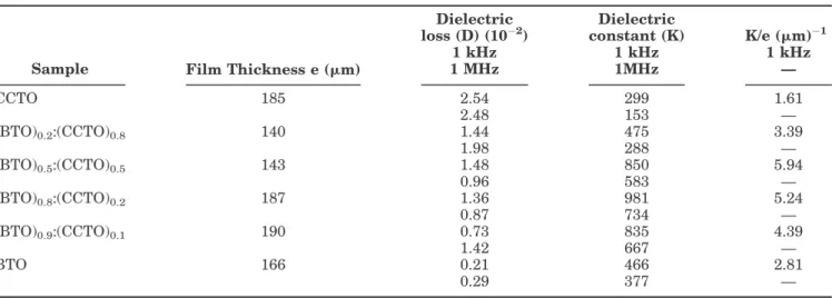
In Fig. 2 are the dielectric constant measurements of the films. The thickness of each film is shown in Table I. The applied electrode diameter is;1 cm for all the films. Note that the BTO film presents a higher K compared to CCTO in the range of frequen-cies under study. At 1 kHz, the value is 466 for the BTO film compared to 299 for the CCTO film (see Table I and Fig. 2). For all the films, the K value always decreases with the increase of the frequency for the range of studied frequencies. However, for the composite film, the result is unexpected. The dielectric constant is higher for all the composites compared to the BTO film for the frequencies under study. The exception is for the (BTO)0.2:(CCTO)0.8 film, which presents a lower value at higher fre-quencies (see Fig. 2). At 100 Hz, the highest value of K is 1187, presented by the composite (BTO)0.8:(CCTO)0.2(see Fig. 2). This K value is dou-ble that of the BTO film. The ratio of the K value to the film thickness (K/e) is also higher for the com-posites. The film (BTO)0.5:(CCTO)0.5 presents the highest ratio of all the films (see Table I).
In Fig. 3 are shown the dielectric losses for these films. At 1 kHz, the loss is higher for the CCTO film
(2.5 3 10 2). When we decrease the amount of CCTO in the film, there is a decrease of the loss. It decreases for the composites and reaches its lowest value for the BTO film (2.1310 2). For all the films, there is a strong dispersion of the loss in this range of frequencies (see Fig. 3). After this initial decrease of the loss, the loss then tends to increase at higher frequencies (Fig. 3). This amazing behavior observed in the dielectric constant (K) for the Fig. 1. XRD patterns of the BTO, (BTO)0.5:(CCTO)0.5, and CCTO
films (Joint Committee on Powder Diffraction Standards (JCPDS), International Center for Diffraction Data, 12 Campus Blvd., Newton Square, PA 19073-3723, USA; 1995), Pattern 93-1880 [BTO-refer-ence], pattern 75-2128 [CCTO-reference].
Fig. 2. Dielectric permittivity (K) as a function of frequency of the films (BTO)x:(CCTO)1 xwith x51, 0.9, 0.8, 0.5, 0.2, 0.
composite film is probably associated with the grain sizes in both phases and with the interfaces between these grains. We are now looking for the presence of this effect in the microwave region as well.
The classic treatment applied for two or more phases present in a dielectric is related to the dielec-tric mixing rules that limit the dielecdielec-tric constant that can be achieved with the mixed phase. The empirical logarithmic rule for the dielectric constant K is given by:26,27
log K5+ I
VIlog KI (4)
where KIis the dielectric constant of the individual phases and VIis the volume fraction of each phase in the composite.
Figure 4 shows the plot of the dielectric constant (K) as a function of the film composition for the MF region and for two frequencies (1 kHz and 1 MHz) obtained from Fig. 6 and the theoretical model based in Eq. 4.
The dash-dot and dotted lines (see Fig. 4) are asso-ciated with the value of K obtained from Eq. 4, at 1 kHz and 1 MHz, respectively (the continuous line is a guide to the eye).
The experimental points (for the frequencies 1 kHz and 1 MHz) of the films are also indicated in the figure. One can easily conclude that addition of BTO increases the K of the film for both frequencies. For both frequencies, note that the composites always present higher values compared to the pure phases. For all the composites, the measured value of the dielectric constant is higher compared to the expected value suggested by Eq. 4. At 1 kHz
the maximum deviation is obtained for the
(BTO)0.8:(CCTO)0.2 film, where the obtained value (K5 981) should be compared to K5427 obtained from Eq. 4 (see Fig. 4). This is unexpected behavior; it means that the composite is not following the lin-ear regime of the model, which indicates a nonlinlin-ear
Table I. Medium Frequency (MF) Measurements of the Dielectric Constant and Dielectric Loss of the Samples (f = 1 kHZ and 1 MHZ)
Sample Film Thickness e (mm)
Dielectric loss (D) (10 2)
Dielectric
constant (K) K/e (mm) 1
1 kHz 1 kHz 1 kHz
1 MHz 1MHz —
CCTO 185 2.54 299 1.61
2.48 153 —
(BTO)0.2:(CCTO)0.8 140 1.44 475 3.39
1.98 288 —
(BTO)0.5:(CCTO)0.5 143 1.48 850 5.94
0.96 583 —
(BTO)0.8:(CCTO)0.2 187 1.36 981 5.24
0.87 734 —
(BTO)0.9:(CCTO)0.1 190 0.73 835 4.39
1.42 667 —
BTO 166 0.21 466 2.81
0.29 377 —
Fig. 3. Dielectric loss (D) as a function of frequency of the films (BTO)x:(CCTO)1 xwith x51, 0.9, 0.8, 0.5, 0.2, 0.
mixing effect of the two phases. In summary, all the films were studied in the medium-frequency range (MF) of the spectra.
Antenna Operation
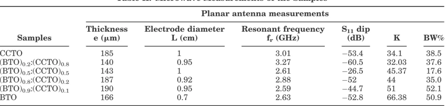
Figures 6–9 show the experimental measure-ments of the S11 parameter of the antennas. This parameter shows the reflections of the signal at the feeding point, the entrance of the antenna. Con-sidering the theoretical model described in Ex-perimental Procedures and using Eqs. 1–3, the dielectric constant and the loss for each antenna was obtained (see Table II). From the analysis of the antenna operation of the samples, one can con-clude that the higher values of the K in the range of
2.5–3.3 GHz antennas is presented due to the BTO substrates (see Figs. 6–9). For the BTO film, the K value is;66 at 2.6 GHz and decreases to 34 for the CCTO film (3 GHz). Starting from the BTO antenna (see Table II), note that the increase of the CCTO presence leads to a decrease of the antenna band-width (BW). For the BTO and CCTO films, the BW is ;50% and ;38%, respectively. For the composite films, the BW value is quite nonlinear. The minimum on the BW factor for the (BTO)0.5: (CCTO)0.5is;17%.
With the presence of CCTO in the samples, this average value of K also decreases to 51 [for the (BTO)0.9:(CCTO)0.1film]. For pure CCTO, the dielec-tric constant is ;34 with BW of 38%. The highest Fig. 5. (a) Experimental setup of the microstrip circular patch antenna. (b) Test device for the return loss of the microstrip circular patch antenna.
Fig. 6. Resonant frequency of the microstrip antenna of sample BTO measured through S11 parameter (return loss). The bandwidth is
obtained at –10 dB, which corresponds to VSWR,2:1.
Fig. 7. Resonant frequency of the microstrip antenna of sample (BTO)0.8:(CCTO)0.2 measured through S11 parameter (return
loss). The bandwidth is obtained at –10 dB, which corresponds to VSWR,2:1.
value for the dielectric constant was obtained for the BTO sample, which was ;66. The lowest one was obtained for the [(BTO)0.2:(CCTO)0.8] sample (K 5 32). The antenna BW is also strongly dependent one the film composition and changes between 17% and 50%.
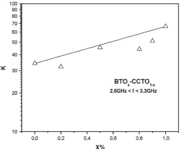
For Fig. 10, the dielectric constant has been meas-ured in the microwave range (2.5–3.3 GHz) for all the films (data obtained from Table II). Note that the dielectric constant is in reasonable agreement with the mixing rule (Eq. 4). Considering the classic treat-ment applied for two or more phases present in a dielectric and the empirical logarithmic rule for the dielectric constant (K) and the dielectric constants (KI) of the individual phases (see Eq. 4), it is possible to conclude that, in the microwave region of the spec-tra, the value of the dielectric constant is in good agree-ment with the rule. However, in the low-frequency region of the spectra, the deviation is quite strong.
The strong dependence of the BW of the antennas, as a function of the film composition in the wave frequencies is certainly related to the micro-structure discrepancies between the two phases present in the film.
Another interesting point observed is that the dielectric constant is following the classic dielectric mixing rules at microwave frequencies (that fix a limit to the dielectric constant that can be achieved with the mixed phase). This is the opposite behavior observed at the MF range, where the composite films do not follow this rule.
CONCLUSIONS
We studied the effect of the presence of CaCu 3-Ti4O12(CCTO) in the dielectric and structural prop-erties of the barium titanate BaTiO3 (BTO) thick film. Films were prepared in two layers using the screen-printing technique on Al2O3 substrates. Mechanical alloying followed by the solid-state pro-cedure has been used successfully to produce pow-ders of CaCu3Ti4O12 (CCTO) that were used in the films. We also looked at the effect of the grain size of the BTO and CCTO in the final properties of the film and studied the dielectric function K and dielec-tric loss of the samples.
The XRD patterns of the films indicate that all of the peaks associated with the BTO phase are present in the films in the tetragonal phase. The
Table II. Microwave Measurements of the Samples
Samples
Planar antenna measurements
Thickness Electrode diameter Resonant frequency S11dip
K BW%
e (mm) L (cm) fr(GHz) (dB)
CCTO 185 1 3.01 53.4 34.1 38.5
(BTO)0.2:(CCTO)0.8 140 0.95 3.27 60.5 32.03 37.6
(BTO)0.5:(CCTO)0.5 143 1 2.61 26.5 45.37 17.6
(BTO)0.8:(CCTO)0.2 187 0.92 2.88 52 44 35.0
(BTO)0.9:(CCTO)0.1 190 0.95 2.59 44.7 51 52.1
BTO 166 0.7 2.63 52.8 66.38 50.9
Fig. 8. Resonant frequency of the microstrip antenna of sample (BTO)0.2:(CCTO)0.8measured through S11parameter (return loss).
The bandwidth is obtained at –10 dB, which corresponds to VSWR,2:1.
Fig. 9. Resonant frequency of the microstrip antenna of sample CCTO measured through S11parameter (return loss). The
CCTO crystallite size is larger when compared with the crystalline size in BTO.18For the kind of films under study, the CCTO film presents the highest value for the crystallite size.
The BTO film was observed to present a higher K compared to CCTO in the range of frequencies under study. At 1 kHz, the value is ;466 for the BTO film compared to 299 for the CCTO film. For all of the films, K value always decreases as the frequency increases, at least for the range of fre-quencies studied herein. However, for the composite film one has an unexpected result. The dielectric constant is higher for all the composites compared to the BTO film for the frequencies under study. This amazing behavior observed for the composite film is probably associated with the sizes of the grains in both phases and related to the interface between these grains. We are now studying the pres-ence of this effect in the microwave region as well.
This surprising observation means that the com-posite is not following the linear regime of the model, which indicates a nonlinear mixing effect of the two phases. From the analysis of the antenna operation of the samples, one can conclude that the higher values of the K in the range of 2.5–3.3 GHz antennas is presented by the BTO substrates. For the BTO film, the value for K is ;66 (2.63 GHz). With the presence of CCTO in the samples ((BTO)0.5:(CCTO)0.5), this average value of the K decreases to 45. For pure CCTO, the dielectric con-stant is ;34 (3 GHz).
From analysis of the antenna operation of the sam-ples, one can conclude that higher K values in the range of 2.5–3.3 GHz antennas are achieved with the BTO substrates (see Figs. 6–10). For the BTO film, the K value is;66 at 2.6 GHz and decreases to 34 for the CCTO film. Starting from the BTO antenna (see Table II), note that the increase of the CCTO pres-ence is leading to a decrease of the antenna BW. For the BTO and CCTO films, the BW values are;50%
and 38%, respectively. For the composite films, the BW value is quite nonlinear. The minimum BW fac-tor for the (BTO)0.5:(CCTO)0.5is;17%.
In general, all resonant antennas will have a limited bandwidth of operation, due to their reso-nant nature.28 Several techniques can be used to increase the BW of resonant antennas and many of these have been used to microstrip patch anten-nas. Lowering the inherent Q factor of the resonator is one such technique. For our antennas, the higher BW presented by the BTO (50.9%) compared to the CCTO (38.5%) (see Table II) is certainly associated with the higher loss presented by the BTO phase, which is a ferroelectric phase.
In summary the performance of a planar micro-strip antenna that uses the (BTO)x:(CCTO)1 xthick film as a high-K substrate was examined. These measurements confirm the potential use of such materials for small high dielectric planar antennas. These materials are also very promising for capaci-tor applications and certainly for microelectronics and microwave devices (cell mobile phones, for example), where device miniaturization is crucial.
ACKNOWLEDGEMENTS
This work was partly sponsored by Ericsson EDB, Ericsson Research Center Brazil, under contract Ericsson-UFC06, and by FINEP, CNPq, FUNCAP, and CAPES (Brazilian agencies).
REFERENCES
1. A. Lozinski, F. Wang, A. Uusima¨ki, and S. Leppa¨vuori, Meas. Sci. Technol.8, 33 (1997).
2. C. Lucat, F. Menil, and R. Von Der Muhll,Meas. Sci. Tech-nol.8, 38 (1997).
3. V. Ferrari, D. Marioli, and A. Taroni,Meas. Sci. Technol.8, 42 (1997).
4. M. Koch, N. Harris, R. Maas, A.G.R. Evans, N.M. White, and A. Brunnschweiler,Meas. Sci. Technol.8, 49 (1997). 5. B. Morten, G. De-Cicco, and M. Prudenziati,Sensors
Actua-torsA31, 153 (1992).
6. N.M. White and V.T.K. Ko, Electron. Lett.(August), 1807 (1993).
7. P. Chahal and R.R. Tummala, IEEE Trans. Compon. Packag. Manuf. Technol.B21 (2), 184 (1998).
8. S. Bhattacharya, R.R. Tummala, P. Chahal, and G. White, 3rd International Symposium on Advanced Packaging Mate-rialsPiscataway, NJ: (IEEE, 1997), p. 68.
9. K. Kinoshita and A. Yamaji,J. Appl. Phys.47, 371 (1976). 10. W.R. Buessem, L.E. Cross, and A.K. Goswami, J. Am.
Ceram. Soc.49, 33 (1966).
11. F.S. Yen and H.I. Hsiang, Jpn. J. Appl. Phys. 34, 6149 (1995).
12. H.I. Hsiang and F.S. Yen, J. Am. Ceram. Soc. 79, 1053 (1996).
13. G. Arlt, D. Hennings, and G.J. With,J. Appl. Phys.58, 1619 (1985).
14. H.I. Hsiang and F.S. Yen, Jpn. J. Appl. Phys. 32, 5029 (1993).
15. M.A. Subramanian, D. Li, N. Duran, B.A. Reisner, and A.W. Sleight,J. Solid. State Chem.323, 151 (2000).
16. A.P. Ramirez, M.A. Subramanian, M. Gardel, G. Blumberg, D. Li, T. Vogt, and S.M. Shapiro,Solid State Commun.115, 217 (2000).
17. M.A. Subramanian and A.W. Sleight,Solid State Sci.4, 347 (2002).
Fig. 10. Dielectric permittivity for the microwave frequency range. Continuous line obtained from Eq. 4 (2.5,f,3.3 GHz). Experi-mental points obtained from Table II (n).
18. A.F.L. Almeida, R.S. de Oliveira, J.C. Go´es, J.M. Sasaki, J. Mendes Filho, and A.S.B. Sombra. Mater. Sci. Eng. B 96, 275 (2002).
19. R.S. de Figueiredo, A. Messai, A.C. Hernandes, and A.S.B. Sombra,J. Mater. Sci. Lett.17, 449 (1998).
20. P. Jha, P. Arora, and A.K. Ganguli, Mater. Lett. 4179, 1 (2002).
21. L.C. Kretly, A.F.L. Almeida, P.B.A. Fechine, R.S. de Oliveira, and A.S.B. Sombra,J. Mater. Sci.: Mater. Electron. 15, 657 (2004).
22. A.F.L. Almeida, P.B.A. Fechine, J.C. Go´es, M.A. Valente, and A.S.B. Sombra, Mater. Sci. Eng., B 111, 113 (2003).
23. E.A. Balanis,Antenna Theory: Analysis and Design, 2nd ed. (New York: John Wiley & Sons, 1997).
24. R. Garg, P. Bhartia, I. Bahl, and A. Ittipiboon,Microstrip Antenna Design Handbook(Artech House, 2001).
25. H. Mosallaaei and K. Sarabandi, IEEE Trans. Antennas Propag.52 (6) (2004), p. 1558.
26. A.J. Moulson and J.M. Herbert,Electroceramics: Materials– Properties–Applications(London: Chapman & Hall, 1990). 27. R.C. Buchanan, ed.,Ceramics and Materials for Electronics:
Processing, Properties and Applications, 2nd ed. (New York: Marcel Dekker, 1991).