N
Abstract — In-circuit testing methodologies are required to tackle the evaluation of embedded radio-frequency circuits. This paper presents design considerations for the test circuitry proposed to implement a methodology for on-chip testing a low-noise amplifier. The scheme being proposed includes an oscillator as the stimulus generator, the re-design of the LNA input switch for test controllability, and an RMS-DC converter to measure the LNA’s output power. Simulation results for 1dB compression and third-order intercept points show a good agreement with the expected ones.
Index Terms — RF, testability and test techniques, low noise amplifier.
I.INTRODUCTION
ew on-chip test methodologies are required to tackle the difficulties found when testing the new generation of integrated systems comprising radio-frequency (RF) circuits. This is particularly true at production stages where the test requirements are not as exhaustive as those required at the developing phase. Lower test equipment cost is enabled by partitioning test resources between on-chip and external equipment. However, new highly structured design for testability (DfT) approaches are necessary to improve accessibility to deeply embedded cores including the RF ones [1].
Different methodologies have been proposed addressing the testing of RF front-ends [2 – 7]. These can be divided in two groups of approaches:
- introduction of test resources within each one of the transceiver blocks
- treating the entire RF front-end as a single block seen from the base-band input and output elements, after creating a loop-back signal path by connecting the PA output into the LNA input.
The techniques in the first group allow diagnosing which blocks in a RF front-end are defective, and to propagate test signals without being affected by the other blocks inserted in the signal path, but imply a higher overhead in test circuitry.
The work presented herein has been partly supported by the Portuguese government, Fundação para a Ciência e a Tecnologia, and carried-out under the framework of projects NanoTEST (2A702 - MEDEA+, phase 2) and Network of Excellence IST-1-507893-NOE TARGET (Top Amplifier Research Groups in a European Team).
J. Machado da Silva, Gabriel Pinho, and J. S. Matos are with Universidade do Porto, Faculdade de Engenharia, and INESC Porto, Campus FEUP, Rª Dr. Roberto Frias nº 378, 4200-465, Porto, Portugal (phone:+351225081400; fax:+351225081443; e-mail: {jms, gabriel, jsm}@fe.up.pt).
On the other hand, the ones in the second group minimize the circuitry overhead but don’t allow identifying which block(s) are behaving incorrectly. Furthermore, some architectures and secondary effects, such as an increase in power consumption, may impair the use of loop-back techniques [7].
In [8] techniques to measure different performance characterization parameters of the low-noise amplifier (LNA) were presented, which rely both on the inclusion of test auxiliary resources and on reusing the functionality of already existing blocks.
One of those techniques consists on applying to the LNA a sequence of stimuli with different amplitudes and measuring the output amplitude for each input level. The obtained set of coordinates (Vin, Vout) allows finding the 3rd
order polynomial that best fits the LNA’s transfer function, i.e., coefficients a0, a1, a2 and a3 in (1).
...
3 3 2 2 1 0+
+
+
+
=
in in in outa
a
ν
a
ν
a
ν
ν
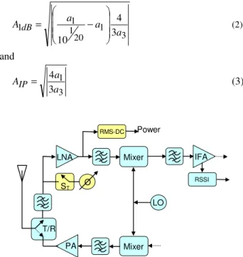
(1)The LNA input voltages which lead to the 1dB compression (P1dB) and third-order intercept (IP3) points are then calculated after the polynomial coefficients using, respectively, 3 1 20 1 1 1 3 4 10 a a a AdB − = (2) and 3 1 3 4 a a AIP = (3) LNA Mixer PA Mixer T/R O LO Power RMS-DC IFA RSSI ST
Fig. 1. Transceiver architecture with LNA’s test infrastructure.
Design for Embedded Testing of a LNA
José Machado da Silva, Gabriel Pinho, José S. Matos
To embed this test scheme in the circuit a typology such the one presented in Fig.1 can be used, where an amplitude controlled oscillator is required to generate the different amplitude stimuli.
The local oscillator (LO) used in the up-converter (mixer) and the power amplifier (PA) itself, can be used to provide this functionality, provided a loop-back scheme exists to connect the PA output to the LNA input, and a scheme to control the signal amplitude is available. In this case the PA’s behaviour has to be taken into account in the characterization of the test stimulus, and eventually the non-linearities of some PA configurations may impair the viability of this solution due to the higher difficulty in obtaining low amplitude stimuli. This would imply also higher power consumption during testing.
To measure the LNA’s output power, logarithmic amplifiers could be used to allow for a wide dynamic variation of the signal power to be represented within a limited voltage range. The received signal strength indicator (RSSI) block existing in typical receivers’ architectures associated to the intermediate frequency (IF) amplifier can also be (re)used for this purpose. But in this case either the mixer behaviour is also included in the measure path, or a switching mechanism has to be included to bypass it. However, as the intermediate frequency is usually much smaller than the LNA’s centre frequency, this approach can be compromised.
One of the advantages brought in by the second group of test approaches described before relies on the testing interface being made mainly at the baseband frequency, and thus avoids interfering and dealing directly with high frequency signals. In order to include a RF test methodology within the global test strategy of the integrated system, using the same test infrastructure, it is desirable that observation and control be made at low frequencies.
The work presented herein addresses the implementation of the method presented in [8], according the scheme shown in Fig.1, i. e., the design of a variable amplitude oscillator (VAO), of the switch to connect it to the LNA input, as well as of the RMS-DC converter to measure the LNA’s output power.
Section II of the paper introduces the LNA to be tested. Sections III to V describe the oscillator, the switch, and the RMS-DC converter to be included in the circuit for testing purposes. Preliminary simulation results are presented in section VI. Finally concluding remarks are highlighted in section VII.
II.THE LNA
Fig. 2 shows the scheme of the LNA to be tested. It is a cascode LNA with inductive source degeneration [9] designed with a 0.18 µm MOS technology, tuned at 435MHz, a frequency used in the standard European
spectrum for general telemetry and telecommand applications. M1 M2 M3 L1 L2 R2 C2 C1 C3 L3 R3 vi vo VDD Ip
Fig. 2 – MOS LNA used in the simulations.
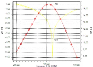
Its nominal characteristics are: input reflection coefficient S11 ≈ -35 dB, power gain S21 ≈ 15dB (Fig. 3), input 1dB compression point Pi1dB = -10 dBm, and third-order interception point IP3 = 0.18 dBm.
Fig. 3 – S11 and S21 parameters of the LNA.
One of the critical aspects in RF on-chip implementations concerns the implementation of spiral inductors on silicon, both in terms of the maximum realisable inductance value and quality factor (Q). Values of L from 1nH to 20nH with Q=5 are common with conventional technologies [9]. Q values up to about 16 have been reported using newer technologies which provide a higher number of metal levels, for frequencies above 2GHz [10].
In the present work the model shown in Fig. 4 is used for the inductors considering Q values around 5. LS and RS are, respectively, the spiral inductance and the series resistance, CS models the feed-through pass created between the two terminals due to direct capacitive coupling, COX is the oxide capacitance between the spiral and the silicon substrate, and RSi represents substrate losses. Although patterned ground
shielding [10] can be used to minimize these losses, it was decided to include them anyway.
LS CS pi RS COX COX RSi RSi po
Fig. 4 – Inductor model used in the simulations.
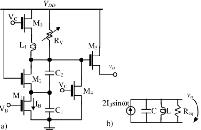
III. AN AMPLITUDE CONTROLLED OSCILLATOR To implement the test stimulus generator a scheme based on the Colpitts oscillator is proposed, as it is one of the tuned schemes used in RF circuits due to its simplicity. Fig. 5 shows the scheme of the oscillator after being improved with facilities to control the amplitude of the output signal, on/off switching (M3, M4), and output buffering (M5).
The output voltage of the Colpitts oscillator is, in a first approach, proportional to the product of bias current (IB) and the net tank equivalent resistance Req (Fig. 5.b). This resistance is actually determined by the inductor’s series parasitic resistance and the overall equivalent resistance seen at the LC tank terminals.
Req L C vo 2IBsinωt a) b) M1 M2 M3 L1 RV C2 vo VDD VB C1 M4 M5 VC VC IB
Fig. 5 – Scheme of the Colpitts based variable amplitude oscillator.
Varying IB would provide a more linear amplitude variation then that obtained varying Req, however, it was found preferable to keep IB constant and to introduce a means to control Req as a wider variation could be attained, namely down to lower voltage levels. This feature is provided by element RV in Fig. 5.a), which basically is a transistor operating in linear mode controlled by its gate voltage. Being the number and amplitudes of the set of stimuli levels to be applied determined, element RV can actually be implemented by a stack of transistors digitally
controlled. This way a, more convenient, digital interface is allowed.
Transistors M3 and M4 operate in switching mode and are used to switch-off the oscillator when the circuit operates in normal mission mode. This facility provides both to avoid power consumption and to create a high impedance output in normal mode (the functionality of switch ST in Fig. 1). Transistor M5 provides output buffering.
The dynamic range required for the oscillator’s amplitude is determined by the LNA’s gain compression characteristic. The different oscillator’s output voltage amplitudes should be distributed with uniform increments below and above the value leading to the 1dB compression point, so that the polynomial (1) that best fits the LNA’s transfer function can be found accurately. For the LNA under consideration the Pi1dB corresponding input voltage value is about 200 mV (-10dBm @ 50 Ω) peak-to-peak.
Fig. 6 – Oscillator’s lowest and highest output levels.
Fig. 6 shows the oscillator output voltage at the lowest and highest levels which correspond to about -21dBm and -2dBm, respectively, observed at the LNA input.
The variable amplitude facility could have been obtained maintaining the oscillator operating with constant amplitude, followed by a variable gain amplifier. This would lead to a larger and, eventually, more power hungry and noisier circuit.
IV. LNAINPUT SWITCHING
The transmit/receive switches used in transceivers circuits are typically implemented using discrete components such as GaAs MESFETs and PIN diodes. Designs using CMOS pass transistors and transmission gates have also been proposed [11], but have the disadvantage of presenting higher insertion loss and nonlinearity. These handicaps can be overcome if transistors are not inserted in the signal path, and are instead used in association with passive devices. A
switch based in this principle is proposed in [12].
However, for frequencies below 1GHz, as Q is lower, the inductance series resistance is responsible for a higher insertion loss which degrades the S21 parameter. To minimize this effect a switch based on a series resonator is used [13]. L1 C1 C2 O IM M1 M2 PA LNA L2 VAO Fig. 7 – Antenna switch.
Fig. 7 shows the scheme of this switch, together with the interface with the VAO and the PA’s output switch (IM block provides for impedance matching with the antenna).
In receiving mode both M1 and M2 are off, leading L1 and C2 to create a series resonator which gives path to the antenna’s signal and whose input and output impedances matches the 50 Ω requirement. In this case the oscillator’s transistor M4 is on, leading M5 to be off and presenting a high impedance output.
In test mode both M1 and M2 are on, leading L1 and C1 to form a parallel tank resonating at the transmitting frequency that creates an open circuit (actually 230 Ω). (The same happens when the PA operates in transmitting mode.) When the switch is open the oscillator can be switched on to apply the test stimulus to the LNA input. As the switch’s output impedance is essentially capacitive, inductor L2 is included to adapt this impedance to the oscillator.
Fig. 8 shows S11 and S21 parameters for LNA including the switch in the receiving mode. The switch exhibits an insertion loss of 0.94 dB in on mode and 10.5 dB isolation in off mode.
Fig. 8 – S11 and S21 LNA’s parameters, including the switch.
Fig. 9 illustrates the waveforms observed at the antenna and LNA inputs, showing that low distortion and low interference are introduced by the input switch, and the VAO.
Fig. 9 – Waveforms at the antenna and LNA inputs.
V. RMS-DCCONVERTER
Fig. 10 shows the scheme of the RMS-DC converter being proposed to detect the LNA’s output rms voltage. Basically it is a half-wave rectifier using a diode-connected P-channel MOS transistors in a common N-well. The bias voltage VB is set to allow measurements to be performed even for the lowest voltage levels. As the test is performed using a known waveform it is easy to relate the measured DC voltage with the actual rms voltage value.
RMS-DC output C1 VDD VB LNA output M C2 R
Fig. 10 – Schematic of the RMS-DC converter.
The measured rms value would not be correct if the LNA operation reaches deep distortion, but, to perform the proposed test it is not necessary to use to high voltage levels. For the highest voltage levels being used, the LNA output waveform starts to compress first for the negative half-cycles. Due to this fact, to obtain a more accurate measure, the negative half-cycles are captured connecting the rectifier’s reference to VDD. A full-wave rectifier would require a more complicated circuit.
VI. TEST SIMULATION RESULTS
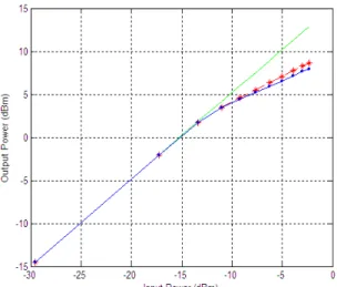
Using the test circuitry presented before, a sequence of 11 equally spaced voltage levels spanning the entire oscillator dynamic range are generated controlling properly the oscillator. Fig. 11 shows the LNA’s power transfer functions obtained observing both the LNA’s (*) and the RMS-DC (•) output voltages, together with the first order ideal characteristic (–). It can be seen that the values obtained with the RMS-DC converter lead to lower output powers for the higher input voltages. This is due, as said before, to the fact that negative cycles start distorting before the positive ones. Anyway, at the point of 1dB compression this effect is still small allowing a measure of P1dB to be obtained with a -0.5dB error. Would the positive cycles be detected instead, the curve given by the RMS-DC converter would be above the LNA’s true curve with a larger error.
Fig. 11 – LNA’s power transfer characteristic obtained observing its output directly (*), using the RMS-DC detector (•), and considering only the linear ideal characteristic.
VII. CONCLUSIONS
Circuits for stimuli generation, switching, and power detection are proposed to implement a method to test a LNA for 1dB compression and third-order interception points. Their development is based on criteria seeking to minimize power consumption and simplicity. Another design driving aspect addresses the facility of controlling the test operation and of observing the output measures using digital or low frequency signals, making it easier to interface this test scheme with general purpose testers.
The performance of these circuits is highly dependent on the characteristics of the technology being used, as well as of the operating frequency. This is the case, namely, of the inductors’ quality factor which can actually be higher at frequencies higher than those considered in this work. This could lead, for example, to opt for another typology to implement the input switch.
In spite of the simplicity of the circuits being proposed, good measurement results can be obtained. This concerns
namely the RMS-DC converter, which is based on a simple half-wave rectifier. Alternative, eventually more accurate, RMS-DC converters or received signal strength indicator circuits would provide more accurate results at the cost of a much higher complexity and power consumption.
Being a controlled oscillator available at the LNA input, the blocks placed after the LNA along the receiver chain can also be tested in sequence.
REFERENCES
[1] International Technology Roadmap for Semiconductors, 2004 Edition. http://public.itrs.net .
[2] Benoît R. Veillette and Gordon W. Roberts, “A Built-In Self-Test Strategy for Wireless Communication Systems”,
Proceedings of the International Test Conference, 1995. [3] E.A. McShane, K. Shenai, B. Blaes, “A monolithic RF
microsystem in SOI CMOS for low-power operation in radiation-intense environments“ Proceedings of the IEEE
Aerospace Conference, Vol. 5, pp. 421-429, March 2000. [4] D. Lupea, U. Pursche, H.J. Jentschel, “Spectral Signature
Analysis – BIST for RF Front-Ends”, Advances in Radio
Science, pp. 155-160, Vol.1, 2003.
[5] R. Voorakaranam, S. Cherubal, A. Chartterjee, “A Signature Test Framework for Rapid Production Testing of RF Circuits”, Proceedings of the Design Automation and Test
Conference in Europe, 2002.
[6] Jerzy Dabrowski, “BiST Model for IC RF-Transceiver Front-End”, 2003, Proceedings of the 18th IEEE International
Symposium on Defect and Fault Tolerance in VLSI Systems
(DFT’03), 2003.
[7] S. Ozev, C. Olgaard, A. Orailoglu, “Testability Implications in Low-cost Integrated Radio Transceivers: A Bluetooth Case Study”, Proceedings of the International Test Conference, 2001.
[8] G. Pinho, J. Machado Silva, H. Mendonça, and J. S. Matos, "A Test Methodology to Compute Typical LNA Characterization Parameters ", Proceedings of the XVIII Conference on Design of Circuits and Integrated Systems, November 2004.
[9] Thomas H. Lee, The Design of CMOS Radio-frequency
Integrated Circuits, Cambridge University Press, 1998. [10] C. Patrick Yue, S. Simon Wong, “Design Strategy of
On-Chip Inductors for Highly Integrated RF Systems”, Proceedings of the Design Automation Conference, 1999. [11] F. Huang, K. O, “A 0.5-µm CMOS T/R Switch for 900-MHz
Wireless Applications”, IEEE Journal of Solid State Circuits, vol. 36, no. 3, pp. 486-492, March 2001.
[12] Niranjan A. Talwalkar, C. Patrick Yue, Haitao Gan, and S. Simon Wong, ”Integrated CMOS Transmit–Receive Switch Using LC-Tuned Substrate Bias for 2.4-GHz and 5.2-GHz Applications”, IEEE Journal of Solid-state Circuits, Vol. 39, No. 6, Juns 2004.
[13] T. Tokumitsu, I. Toyoda, M. Aikawa, “Low Voltage High Power T/R Switch MMIC Using LC Resonators”, IEEE
Microwave and Millimeters-Wave Monolithic Circuits Symposium, pp. 27-30, 1993.