*e-mail: [email protected]
1. Introduction
Transparent conductive oxides (TCOs) are fundamental components in optoelectronic applications1-3. TCO materials have the ability to couple two important features for applications in the optoelectronic devices industry; an optical transmittance of around 80% in the visible region and low electrical resistivity of around 10–3 to 10–4Ω cm[1-3]. Indium tin oxide (ITO) is currently the most widely used TCO for optoelectronic devices. However, indium, the main chemical component of ITO, is scarce in nature and consequently the production cost of ITO is relatively high3-5.
Therefore, there is an incentive to ind an alternative to ITO.
Zinc oxide (ZnO), a promising alternative to ITO, is an n-type semiconductor and, can therefore easily be doped with group III elements, such as aluminum and gallium. The advantages of ZnO include an optical gap of 3.3 eV, low toxicity, good optical and electrical properties, and chemical stability in plasma processes1-3. In addition, zinc is abundant in nature; consequently, ZnO is relatively cheap.
ZnO:Al and ZnO:Ga thin ilms have been produced by a
wide variety of techniques, including chemical and physical processes, such as pulsed laser deposition6, chemical vapor deposition7, spray pyrolysis8, sol-gel technique9, atomic layer deposition10 and magnetron sputtering11 onto a variety of substrates. Among these methods, magnetron sputtering is especially interesting, because it can not only be conducted at low temperatures, but can also produce high-quality
crystalline intrinsic and doped ZnO thin ilms12. Moreover,
this technique allows the deposition of thin ilms on large
areas of substrate.
The surface morphology of a thin ilm may indicate its
dynamic growth13-15. Typically, growth of a thin ilm is a non-equilibrium process, which can lead to the formation of a roughened surface with granular or pyramidal structures4,13,15. Moreover, the properties of the surface of
a thin ilm, especially the surface roughness, may strongly inluence their applications4,13,16. There are also intrinsic relations between the surface morphology and other factors,
such as crystalline structure and ilm thickness, which have
been found to play important roles in determining physical
and chemical ilm properties15,17.
Films having a high native surface roughness can be
beneicial for light trapping in solar cell applications16.
In other applications, however, different thickness/
roughness ratios are required; for example, smooth surfaces are preferred for electronic devices18. This makes the understanding the surface evolution and its correlation
with electrical and optical properties mandatory for speciic ZnO thin ilm applications. In this work, aluminum-doped zinc oxide thin ilms were grown on glass substrates using
reactive RF magnetron sputtering of a zinc-aluminum
target. The surface evolution of the ilms and their optical
and electrical properties were investigated as a function of
ilm thickness.
Morphological and Electrical Evolution of ZnO:Al Thin Films Deposited by
RF Magnetron Sputtering onto Glass Substrates
Érica Pereira da Silvaa, Michel Chavesa, Steven Frederick Durranta, Paulo Noronha Lisboa-Filhob,
José Roberto Ribeiro Bortoletoa*
aTechnological Plasmas Laboratory, São Paulo State University – UNESP, Av. Três de Março, 511, Alto da Boa Vista, CEP 18087-180, Sorocaba, SP, Brazil
bGroup of Advanced Materials, São Paulo State University – UNESP, Av. Eng. Luiz Edmundo Carrijo Coube, 14-01, Núcleo Habitacional Presidente Geisel, CEP 17033-360, Bauru, SP, Brazil
Received: March 22, 2014; Revised: September 11, 2014
In this work, the surface and electrical characteristics ZnO:Al thin ilms deposited by RF magnetron
sputtering onto glass substrates have been investigated. Analysis of surface morphologies revealed
two growth stages. In the irst stage, up to thicknesses of 100 nm, the ilms show surface structures with a granular form without preferential orientation. Beyond thicknesses of 100 nm, however, the
grain structures increase in size and height, producing a pyramidal form and preferred orientation along the c-axis. The XRD results show that the ilms have a preferred orientation in the (002) plane.
Furthermore, with the evolution of the ilm thickness the electrical resistivity decreases to a minimum
of 1.6 × 10⁻³Ω cm for the ilm of 465 nm thickness. The doping with aluminum atoms produces an increase in concentration of charge carriers to around 8.8 × 1019 cm–3. All ilms exhibit high optical transmittance (above 85%) in the visible region.
2. Experimental
The deposition system consists of a cylindrical 304 stainless steel chamber of 270 mm diameter and 200 mm
in height. Films of ZnO:Al were deposited on 1mm-thick
glass substrates by RF magnetron sputtering. Before loading in the sample holder the glass substrates were ultrasonically cleaned in deionized water with detergent (Det limp S32) for 8 min. After that the substrates were subjected to a second ultrasound bath containing only distilled water,
and inally the substrates were subjected to an isopropyl
alcohol bath. A metallic zinc-aluminum (1 wt% of Al) target of 99.99% purity was used. The plasma was maintained using a forward 13.56 MHz (RF) power of 100 W. In all depositions the substrate-holder was polarized. An argon pressure of 6.7 Pa was employed. A substrate temperature of 373K was maintained during the growth. To study the
growth evolution, different ZnO:Al ilms with thicknesses
ranging from 0 up to 465 nm were deposited.
Surface morphology was measured using atomic force
microscopy (AFM, XE-100, Park Systems) operating in air.
The scanned area was 2 mm × 2 mm with 512 × 512 pixels. The parameters of surface roughness (σ) and correlation length (ξ) were obtained from the surface morphology measured using AFM. Surface roughness is mathematically
deined by Equation 119.
(
)
21
1 N i i
h h
N =
σ = ∑ − (1)
In this equation N is the number of pixels, hi the individual heights, and <h> the mean height.
Furthermore, the average value of correlation length ξ
was derived by itting by a Lorentzian curve to the power
spectral density (PSD) calculated from AFM images. The correlation length ξ is usually related to the lateral size evolution of the surface structures.
Optical transmittance spectra were obtained using a
Uv-Vis-NIR spectrometer (Lambda 750, Perkin Elmer) over
the 190 nm to 3300 nm wavelength range. The electrical resistivity was measured by the four-point probe method at room-temperature. An X-ray diffractometer
(D/MAX-2100/PC, Rigaku) was used to determine the degree of crystallinity of the ZnO thin ilms.
3. Results and Discussions
Table 1 shows the values of morphological, optical
and electrical properties obtained for the ZnO:Al ilms as a function of ilm thickness.
Figure 1 allows comparison of XRD spectra obtained
for the ilm of ZnO:Al (of thickness 465 nm) and of the intrinsic ZnO ilm. The intrinsic ZnO ilm was also obtained by RF magnetron sputtering, and possesses a thickness of 550 nm. Both the ZnO:Al ilm (465 nm) and the intrinsic ZnO ilm exhibit a preferred orientation along the c-axis, perpendicular to the substrate surface in the plane (002), which, according to the JCPDS (65-3411) table, corresponds to a wurtzite ZnO structure.
The average crystallite size parallel to the ilm surface
can be estimated by an analysis of the full width at half
maximum (FWHM) and maximum peak position, as
observed in the XRD spectra, using Scherrer’s equation20:
cos Kl
τ =
b θ (2)
where K represents a shape factor, that normally has a value of 0.9[20], l is the wavelength of the X-rays, b is the value
of the FWHM of the (002) plane peak and θ corresponds to the Bragg angle. The incident wavelength used was 1.5405 Å. Using the data in Scherrer’s formula the average crystallite size (τ) of the intrinsic ZnO ilm was found to be
17.7 ± 0.1 nm. When the ilm was doped with aluminum,
however, the crystallite size decreased to 8.1 ± 0.1 nm. Furthermore, it is clear from observation of Figure 1 that
the intensity of the peak corresponding to the (002) plane
decreased with doping, while the FWHM value roughly doubled.
Table 1. Structural, electrical and optical properties of the ZnO:Al thin ilms as a function of the thickness.
Properties/Sample Substrate S1 S2 S3 S4 S5 S6
Thickness (nm) 0 25 50 100 185 250 465
Roughness (nm) 1.71 2.10 2.26 5.3 8.3 9.9 19.5
Correlation length (nm) 0.11 0.072 0.067 0.094 0.14 0.16 0.29
Resistivity (10–3 Ω cm) -- -- 8.6 5.7 1.8 1.6 1.6
Refractive index at 550 nm 1.51 2.01 2.09 2.1 2.10 2.06 2.0
Transmittance at 550 nm (%) 91.6 91.5 88.8 83.8 85.8 85.9 84.7
Figure 1. XRD spectra of intrinsic ZnO and ZnO:Al ilms deposited
It may be noted from the diffraction spectra that there is a difference in the values of the Bragg angle. The (002)
plane of the intrinsic ZnO ilm is attributed to the peak at
θ = 34.35°, close to the default value given in the JCPDS table (θ = 34.43°). The peak attributed to the (002) plane
of the ZnO:Al ilm, however, appears at smaller angles
(θ = 34.04°). The presence of residual compressive stress in the crystal lattice of ZnO, inferred from the reduction in
θ, inluences the dynamic growth of the grains.
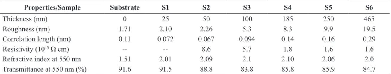
Figure 2 shows AFM surface images of the ZnO:Al ilms
of different thicknesses deposited onto glass substrates. The
surface morphology is found to evolve homogeneously with well-distributed structures. Initially, the surface morphology
is mainly formed by small granular structures. Beyond ilm thicknesses of about 100 nm, these structures increase in
both height and width, until faceted structures are produced. As shown in Figure 3, AFM images obtained for the
ilms with thicknesses of 50 nm and 250 nm show the
differences between the surface structures. The lateral
proile obtained for each image makes clear the growth of
the structures in both height and width. Similar behavior
has been reported by Vasco et al for ZnO/InP (100) ilms grown by PLD technique15. The same authors also reported
the presence of two growth stages. In the irst stage with short deposition times (corresponding to thickness of up to
200 nm) formation of granular structures occurs. Beyond 200 nm, as the deposition time increases a second stage is observed, where the structures are developed both in width and in height, and have a six-folded pyramidal shape15.
From the AFM images the surface roughness was
determined as a function of ilm thickness. The results are
shown in Figure 4. The RMS roughness of ZnO:Al thin ilms
increases with increasing thickness due to the formation of
a textured surface with pyramidal structures.
A similar dependence of the roughness on the thickness
was also reported by Vasco et al.15 (ZnO/InP), Seo et al.21 (AGZO/glass) and Wang et al.17 (AZO /Si/quartz). Vasco et al.15, however, reported that the roughness of the
ZnO/InP ilms continuously increases up to 240 nm in thickness and stabilizes from 400 nm due to development of
the stepped facets in the pyramidal structures. Probably due to substrate bias polarization, similar stabilization was not
observed here, at least until a thickness of 465nm. As also
observed in the present study, Seo et al.21 reported a sharp
rise in roughness for thicknesses beyond 100 nm.
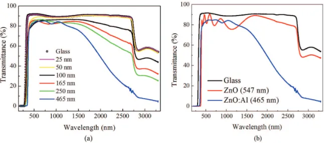
The main issues for the application of ZnO ilms as TCOs
are high optical transmittance (above 80%) in the visible region and low resistivity (of about 10–3 to 10–4Ω cm). In this context, Figure 5a shows the optical transmittance of
ZnO:Al thin ilms as a function of wavelength for various thicknesses. Figure 5b shows transmission spectra of glass,
ZnO and ZnO:Al ilms. Figure 5a shows a high optical
transmittance (more than 85%) for the ilms of ZnO:Al
in the visible range. According to Table 1, the refractive
index for all ilms averaged 2.06 at 550 nm. Figure 5a also shows a decrease in optical transmittance from 1500 nm
for the ilm with 465 nm thickness. The reduction in optical
transmittance in the infrared region is most probably related
to an increase in light relection due to an increased charge carrier density. It is known that TCOs behave as metallic materials in the infrared region, and thus are relective2. Furthermore, it is possible to observe in Figure 5b that the
intrinsic ZnO ilm is transparent in the infrared region even when thicker than the ZnO:Al ilm.
From the optical transmission spectra it was possible to determine the value of the energy gap (EG) using Equation 322.
Figure 2. AFM images of glass substrate and ZnO:Al thin ilms grown to various thicknesses. (a) Glass substrate, (b) 25 nm, (c) 100 nm,
1/ 2
( g)
h B h E
α ν = ν − (3)
where α is the absorption coeficient, hv corresponds the photon energy, B is a band edge constant and the exponent of 1/2 corresponds to allowed direct transitions. As shown in Figure 6, the optical band gap can then be obtained from
the intercept of (ahν)2 versus hν for direct transitions. The values of the EG were determined by extrapolating the linear portion of the curves to α = 0.
As derived from Figure 6, the energy gap of the intrinsic
ZnO ilm of ~3.28 eV is in agreement with literature values. The ilm of ZnO:Al (465 nm) showed an increase in the
gap to around 3.47 eV. This increase is related to the Moss Burstein effect23,24. When the number of critical charge carriers is exceeded in a n-type semiconductor, the Fermi
level moves toward the conduction band by illing its lower
states. Consequently an extension of the optical gap occurs and a higher excitation energy will be required for an electronic transition from the valence band to an unoccupied state of the conduction band23,24. The shift of the Fermi level to the conduction band can be described by Equation 423.
2/3 2
2/3 *
3 8 n
c
h
E N
m
∆ = π
(4)
where * c
m is the effective mass of conduction, which for ZnO is equal to 0.38[23], h is Planck’s constant, and N is the carrier density. Therefore, the carrier density of the doped
ilm can be obtained knowing that the energy variation (∆EN)
between the intrinsic ZnO ilm (3.28 eV) and the doped ilm (3.47 eV) is equal to 0.19 eV. It is known that the intrinsic ZnO ilm has a carrier density of 5.9 × 1018 cm–3[23], and with
doping the carrier density of the ZnO:Al ilm increases to
8.8 × 1019 cm–3.
Figure 3. Surface AFM images (2 mm × 2 mm ) and lateral proiles of the ZnO:Al thin ilms with (a) 50 nm and (b) 250 nm of thickness.
Figure 4. RMS roughness of the ZnO:Al ilms as a function of
Figure 7 shows the evolution of the lateral size of the
grains, structures and the electrical resistivity with ilm thickness. The increase in charge carriers contributes to the
decrease of the electrical resistivity. However, the resistivity
depends on the thickness of the ZnO:Al ilms.
The Mayadas-Shatzkes theoretical model describes the dependence of resistivity on ilm thickness for polycrystalline thin ilms25. In his model, Mayadas-Shatzkes attributes the increase in resistivity to the scattering of electrons at grain boundaries25. Furthermore, Mayadas-Shatzkes assumes two cases for grains structures25. For ilms that show grain structures in column format, with a constant diameter, the
resistivity of the material is independent of thickness25. For
ilms that show structures with different grain diameters, however, the resistivity is dependent on the thickness25. As shown in Figure 7, the lateral size increases as a function
of thickness. These results indicate that the ilms have grain
structures with different diameters. Furthermore, the curve of electrical resistivity followed the trend expected for the second case cited above. Consequently, the mechanism that
is inluencing the resistivity of ZnO:Al ilms is the scattering
of electrons at the grain boundaries.
According to Figure 7, a reduction of the lateral size
for ilms with smaller thicknesses than 50 nm is observed.
Films with smaller grain structures indicate an increase in defects at the grain boundaries, which increases the scattering of electrons and decreases the electronic mobility.
For thicknesses above about 100 nm, however, an increase
in lateral size occurs. This result indicates an improvement
in crystallinity of the ilm and a decrease in the grain
boundaries defects, with a consequent increase in electron mobility which in turn reduces the electrical resistivity.
From the data obtained of the carrier density (8.8 × 1019 cm–3) and electrical resistivity (1.6 × 10⁻³Ω cm) it was possible to determine the value of the electron mobility (mE) for the thicker ZnO:Al ilm (550 nm) using Equation 5.
1 e
ne
µ =ρ (5)
Figure 5. (a) Optical transmittance of ZnO:Al thin ilms as a function of ilm thickness. (b) Transmission spectra of the glass substrate,
ZnO:Al (465 nm) and intrinsic ZnO (550 nm) thin ilms.
Figure 6. The energy gap of the ZnO:Al and intrinsic ZnO ilms
estimated by the extrapolation of the linear part of the (ahν)2
versus hν plots.
Figure 7. Lateral size calculated from a Lorentz itting of the 2D
were ρ is the electrical resistivity, n is the number of charge carriers and e corresponds to the electronic charge. The
electron mobility of ZnO:Al ilm is ~ 44 cm2/Vs.
The corresponding resistivity curve, however, tends to stabilize at 1.6 × 10⁻³Ω cm and, therefore, the electron mobility stabilizes at 44 cm2/V.s. This limitation may be caused by defects in the crystal lattice of ZnO related to the aluminum atoms. These defects act as electron scattering centers and reduce the electron mobility. Indeed, the electron mobility is predicted to be about 50 cm2/Vs for an aluminum doping concentration of 1020 cm–3 when the ionized impurity scattering mechanism is considered1.
4. Conclusions
ZnO:Al thin ilms were deposited onto glass substrates
by RF magnetron sputtering. Surface morphology exhibits a transition between small grain structures of
granular shape to grain structures of pyramidal shape.
The XRD results showed that the ilms have a preferred
crystal orientation in the (002) plane, along the c-axis
perpendicular to the substrate surface. As the thickness of the ilms increases an increase in lateral grain size occurs
and, consequently, an improvement in the crystallinity is obtained. On the other hand, the resistivity tends to
decrease with increasing thickness to a minimum value
of 1.6 × 10⁻³Ω cm. In addition, the ilms exhibited a good optical transmittance of more than 85% in the visible region.
Acknowledgements
The authors acknowledge the inancial support of the
Brazilian agencies FAPESP (2008/53311-5, 2011/21345-0) and CNPq (555774/2010-4, 301622/2012-4).
References
1. Ellmer K, Klein A and Rech B, editors. Transparent conductive
zinc oxide: basics and applications in thin ilm solar cells. New York: Springer; 2008. Springer Series in Materials Science, v. 104. http://dx.doi.org/10.1007/978-3-540-73612-7.
2. Ginley DS, Hosono H and Paine DC, editors. Handbook of transparent conductors. New York: Springer; 2010. 3. Liu H, Avrutin V, Izyumskaya N, Özgür Ü and Morkoç H.
Transparent conducting oxides for electrode applications in light emitting and absorbing devices. Superlattices and Microstructures. 2010; 48(5):458-484. http://dx.doi. org/10.1016/j.spmi.2010.08.011.
4. Zhu H, Mai Y, Wan M, Gao J, Wang Y, He T, et al. Study of back reflectors for thin film silicon solar cells. Thin Solid Films. 2013; 539:284-289. http://dx.doi.org/10.1016/j. tsf.2013.05.019.
5. Tseng CA, Lin JC, Weng WH and Lin CC. Photoelectron spectroscopy and optical properties of Al-Doped ZnO films prepared by sputtering with radio frequency power applied to Al target. Japanese Journal of Applied Physics. 2013; 52(2R):025801. http://dx.doi.org/10.7567/JJAP.52.025801.
6. Fazio E, Patanè S, Scibilia S, Mezzasalma AM, Mondio G, Neri F, et al. Structural and optical properties of pulsed laser deposited ZnO thin films. Current Applied Physics. 2013; 13(4):710-716. http://dx.doi.org/10.1016/j.cap.2012.11.010. 7. Ding K, Hu QC, Wang X, Zhang JY, Lin WW, Lin CS, et al.
Aluminum doping induced columnar growth of homoepitaxial ZnO films by metalorganic chemical vapor deposition.
Applied Physics Letters. 2013; 103(14):141907. http://dx.doi. org/10.1063/1.4824116.
8. Ortel M, Balster T and Wagner V. Chemical composition and temperature dependent performance of ZnO-thin film transistors deposited by pulsed and continuous spray pyrolysis.
Journal of Applied Physics. 2013; 114(23):234502. http:// dx.doi.org/10.1063/1.4846736.
9. Ammaih Y, Lfakir A, Hartiti B, Ridah A, Thevenin P and Siadat M. Structural, optical and electrical properties of ZnO: Al thin films for optoelectronic applications. Optical and Quantum Electronics. 2014; 46(1):229-234. http://dx.doi.org/10.1007/ s11082-013-9757-2.
10. Kim KW, Son HS, Choi NJ, Kim J and Lee SN. Growth and characterization of polar and nonpolar ZnO film grown on
sapphire substrates by using atomic layer deposition. Thin Solid Films. 2013; 546:114-117. http://dx.doi.org/10.1016/j. tsf.2013.03.071.
11. Bikowski A, Welzel T and Ellmer K. The correlation between the radial distribution of high-energetic ions and the structural as well as electrical properties of magnetron sputtered ZnO: Al films. Journal of Applied Physics. 2013; 114(22):223716. http://dx.doi.org/10.1063/1.4840975.
12. Wu HW, Yang RY, Hsiung CM and Chu CH. Characterization of aluminum-doped zinc oxide thin films by RF magnetron sputtering at different substrate temperature and sputtering power. Journal of Materials Science Materials in Electronics. 2013; 24(1):166-171. http://dx.doi.org/10.1007/s10854-012-0769-7.
13. Karabacak T. Thin-film growth dynamics with shadowing and re-emission effects. Journal of Nanophotonics. 2011; 5(1):052501. http://dx.doi.org/10.1117/1.3543822.
14. Kajikawa Y. Texture development of non-epitaxial polycrystalline ZnO films. Journal of Crystal Growth. 2006; 289(1):387-394. http://dx.doi.org/10.1016/j. jcrysgro.2005.11.089.
15. Vasco E, Zaldo C and Vázquez L. Growth evolution of ZnO films deposited by pulsed laser ablation. Journal of Physics Condensed Matter. 2001; 13(28):L663-L672. http://dx.doi.
org/10.1088/0953-8984/13/28/102.
16. Chen XL, Wang F, Geng XH, Zhang DK, Wei CC, Zhang XD, et al. Natively textured surface Al-doped ZnO-TCO layers with gradual oxygen growth for thin film solar cells via magnetron sputtering. Applied Surface Science. 2012; 258(8):4092-4096. http://dx.doi.org/10.1016/j. apsusc.2011.12.061.
17. Wang F, Wu MZ, Wang YY, Yu YM, Wu XM and Zhuge LJ. Influence of thickness and annealing temperature on the electrical, optical and structural properties of AZO thin films. Vacuum. 2013; 89:127-131. http://dx.doi.org/10.1016/j. vacuum.2012.02.040.
18. Betz U, Kharrazi Olsson M, Marthy J, Escolá MF and Atamny F. Thin films engineering of indium tin oxide: Large area flat panel displays application. Surface and Coatings Technology. 2006; 200(20-21):5751-5759. http://dx.doi.org/10.1016/j. surfcoat.2005.08.144.
deposited by RF magnetron sputtering. Journal of Physics: Conference Series. 2012; 370(1):012020. http://dx.doi. org/10.1088/1742-6596/370/1/012020.
20. Avril L, Guaino P, Maseri F, Muthukaruppasamy K and Pireaux JJ. Correlation between the electrical and structural properties of aluminium-doped ZnO thin films obtained by direct current magnetron sputtering. Journal of Physics: Conference Series. 2013; 417(1):012011. http://dx.doi.org/10.1088/1742-6596/417/1/012011.
21. Seo K-W, Shin H-S, Lee J-H, Chung K-B and Kim H-K. The effects of thickness on the electrical, optical, structural and morphological properties of Al and Ga co-doped ZnO films grown by linear facing target sputtering. Vacuum. 2014; 101:250-256. http://dx.doi.org/10.1016/j.vacuum.2013.09.009. 22. Vinodkumar R, Navas I, Chalana SR, Gopchandran KG,
Ganesan V, Philip R, et al. Highly conductive and transparent
laser ablated nanostructured Al: ZnO thin films. Applied Surface Science. 2010; 257(3):708-716. http://dx.doi. org/10.1016/j.apsusc.2010.07.044.
23. Roth AP, Webb JB and Williams DF. Absorption edge shift in ZnO thin films at high carrier densities. Solid State Communications. 1981; 39(12):1269-1271. http://dx.doi. org/10.1016/0038-1098(81)90224-6.
24. Singh B, Khan ZA, Khan I and Ghosh S. Highly conducting zinc oxide thin films achieved without postgrowth annealing.
Applied Physics Letters. 2010; 97(24):241903. http://dx.doi. org/10.1063/1.3525575.
25. Philipp M. Electrical transport and scattering mechanisms in