XXXVIII Figure 2.30 – Band-pass filter to clean the signal spectrum on the ADC's input……….XXXVIII Figure 2.31 – Low-pass filter to attenuate the LO tone inserted in the second mixing stage………..XL Figure 3.1 – Internal composition of the FPGA block… …….XLII. XLVIII Figure 3.4 – Simplified example of a symmetric systolic parallel FIR implementation………..XLIX Figure 3.5 – Frequency response of the FIR equalizer designed……….L Figure 4.1 – Architecture to be used to construct block B.
Acronyms List
Introduction
- Introduction
- Filter Specifications
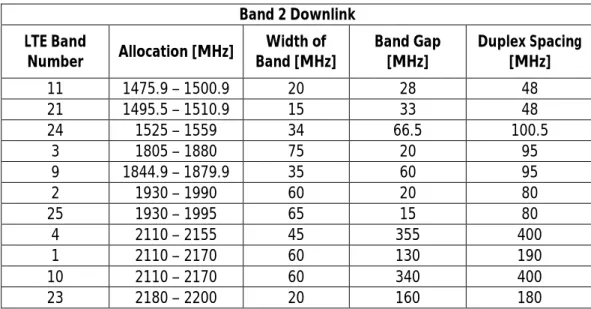
- LTE Bands
- Band 1
- Band 2
- Band 3
- Non Supported Band
- General Architecture
- Dissertation Outline
In the following section, an overview of the LTE bands and their division into the 3 decided major bands is given. A comparison is also performed between the simulation of the FPGA in Matlab (software simulation) and in Xilinx ISE (Integrated Software Environment) (hardware simulation).
Downconversion
- Introduction
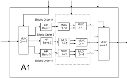
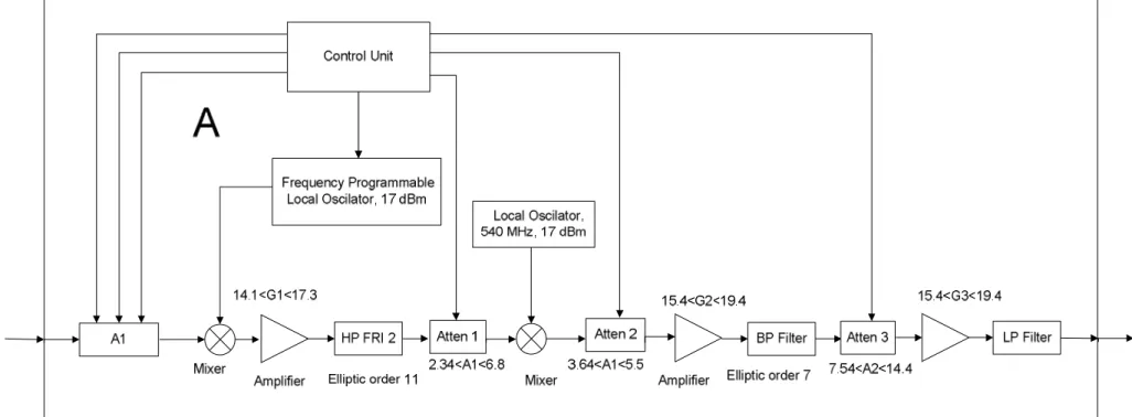
- Downconversion Block (Block A)
- Downconversion Block SNR
- Downconversion Block initial SNR
- Mixers
- Up mixing and Down Mixing
- Mixing modes and concepts
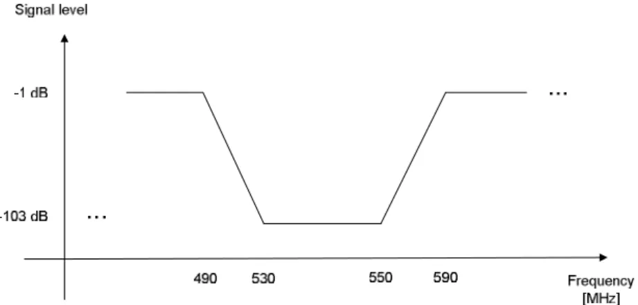
It is then determined that the minimum value of the signal spectral density is -77.4 dB at the beginning of the downconversion block. Moreover, the insertion loss of the attenuator is usually 1.1 dB and it is at most 2.5 dB.
Continuous non-linear mode
In this case it would be impossible to filter most of the third order products mentioned above because they will be mixed exactly in the desired frequency band or very close to this frequency band. The third order intercept point (TOIP) is a theoretical point where the output level of a third order intermodulation product is equal to the output level of the fundamental.
Switching Mode Mixers
If the power at the input of the mixer is too high, the output will reach a maximum level, it will saturate, meaning that both the fundamentals and intermodulation harmonics will tend to increase very little or remain constant with increasing power input (see figure 2.8). The 1 dB compression point is the point where the input power is increased, but the base output power is 1 dB below what it would be if the power at the mixer input were low enough for that device to operate linearly. The region.
Double-Balanced Mixers
Noise Figure
Thus, it can represent a measure of the noise added by the mixer, the noise that is converted to the IF output. As a result, noise in the non-signal sideband (image band) will be added to the IF output.
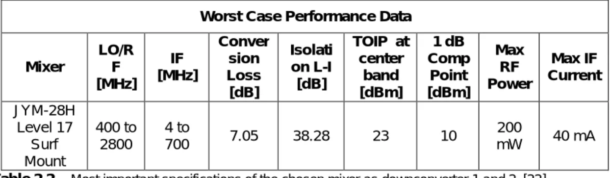
Downconversion Mixer Selection
For our purposes (frequency bands used), the minimum conversion loss of the mixers used is 5.76 dB and its maximum conversion loss is 7.05 dB, which is shown in Table 2.2.
Down Conversion Process .1 First Step
Introduction
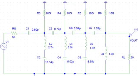
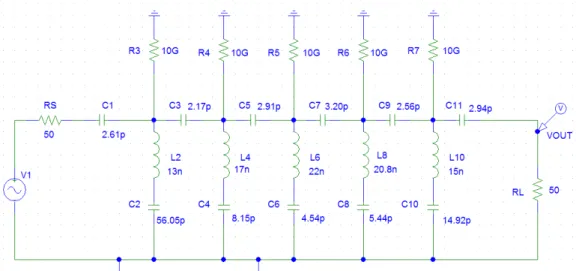
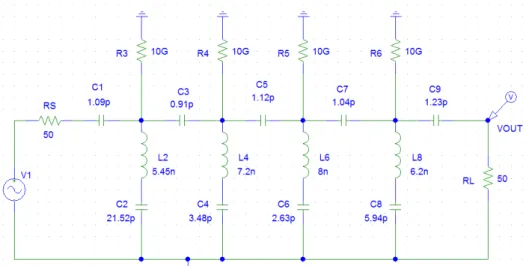
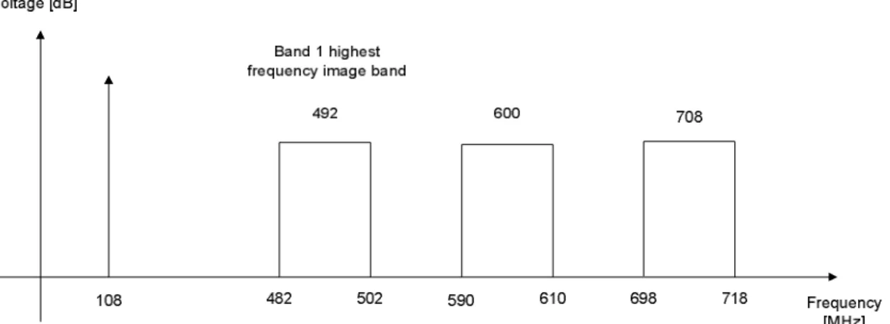
It was chosen to reject the image band for the entire large band instead of rejecting the image band for the selected LTE band, because that way the filter architecture becomes simpler (less order) and much more flexible. The image rejection high-pass filters for each band are exhibited in the upcoming subsections.
Major Number of Band and Matching Image Band Rejection
High Pass Band 1
To evaluate the performance (degradation) of filters with biased parameters, the market characteristics of their components were used in the simulations.
High Pass Band 2
High Pass Band 3
Second Step
Looking at Figure 2.24, it is clear that there must also be an image rejection filter for this down conversion step.
Pre-Processing Before the Analog to Digital Conversion
Band Pass Filter
Low Pass Filter
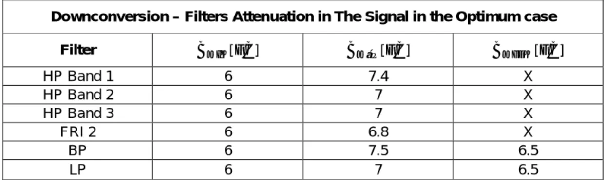
Simulated range of the Attenuation filters in the Down conversion Block
The attenuation the signal suffers when passing through the down-conversion block filters usually increases when the components of the filters do not have ideal values. The ideal attenuation (ideal case) and very bad case attenuation are given in Tables 2.3 and 2.4 respectively. These attenuations account for the limited frequency bands occupied by the signal before passing through each filter.
FPGA Block
- Introduction
- Digital Filter
- Digital Filter Higher Level Design for the FPGA
ENOB specifies the number of bits in the digitized signal above the noise floor of the ADC. The conclusions to be drawn are therefore that the ENOB and the typical INL error are the parameters that limit the performance of the ADC. In terms of operating errors (other than noise and distortion), 13 bits of the ADC are typically 100% reliable.
![Table 3.1 – Most important specifications of the chosen ADC including noise and distortion but excluding error specifications [29]](https://thumb-eu.123doks.com/thumbv2/123dok_br/19768782.0/44.892.160.744.125.219/table-important-specifications-chosen-including-distortion-excluding-specifications.webp)
Digital Filter High Level Architecture
Digital Filter Lower Level Design for the FPGA
They all have different strengths and weaknesses and all will be studied so that the circuit that best meets our goals can be selected. There are serial FIRs, parallel FIRs which divide into 2 categories, transposed and systolic filters and finally there are semi-parallel FIRs. An example of a serial FIR and an example of a transposed FIR can be seen in the appendix, section 3.4.
Systolic FIRs
Symmetric Systolic FIRs
The semi-parallel FIR architecture study will not be shown because there are no hardware limitations and parallel architectures work faster. At the top left of the picture, the bus begins, where the samples are loaded.
FIR Design in FPGA Conclusions
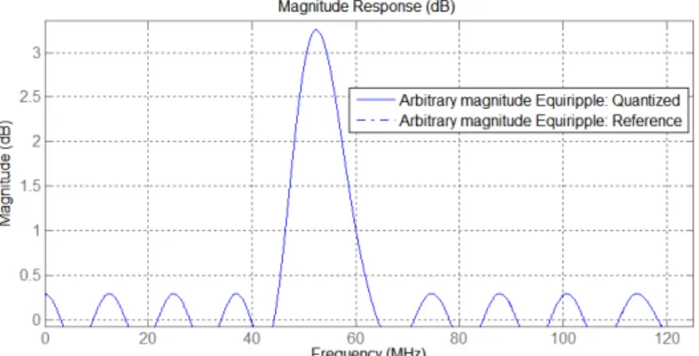
Equalizer
The specifications in frequency of the Equiripple equalizer projected were those presented in table 3.5. It is certain that these harmonics cause errors in the 14th bit of the DAC (IMD) and they can possibly affect bits 13th and 12th (SFDR). This is possibly a good approximation of the signal present at the output of the ADC.
Upconversion
- Introduction
- Upconversion Block (Block B)
- Upconversion Block SNR
- Up Conversion Process .1 First Step
- Second Step
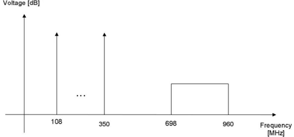
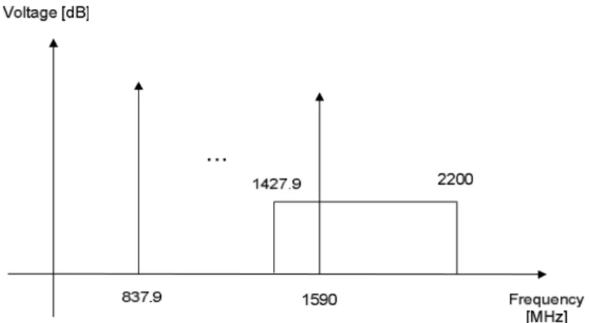
The first and last muxes guide the signal through the image suppression filter of the corresponding main band in which the signal is located. The maximum level of the signal was -94.64 dB/Hz (LTE band was initially centered in 2350 MHz components with ideal values). These sections are defined exactly as in section 2.2 of the thesis and the same parameters are taken into account to calculate the SNR degradation of each section.
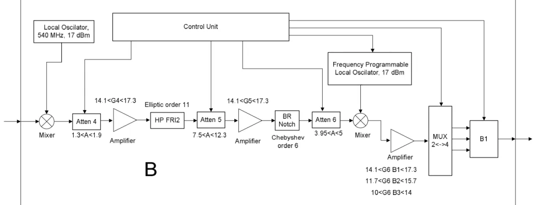
Variable LO tone Rejection
Now touching on a tangent topic, the absence of the need for further attenuation of the LO tone introduced in the first up-conversion step will now be demonstrated. The LO tone introduced in the first up-conversion mixing step will be called LO1 exactly as it was done for the down-conversion process. Let's go back to rejecting the variable LO tone added in the second up-conversion step.
Bands and Sub Bands
In the case of variable LO rejection, the transition band of the filters is often at a much higher frequency, and the filter will require a significantly larger transition band to compensate (order . <11). In all these types of filters, a transition band of approximately 300 MHz or higher will be used. To allow the filters to have transition bands of that size, band 2 is divided into 3 sub-bands and band 3 into 2 sub-bands.
Calculations of the minimum attenuations required for the several LO rejection filters
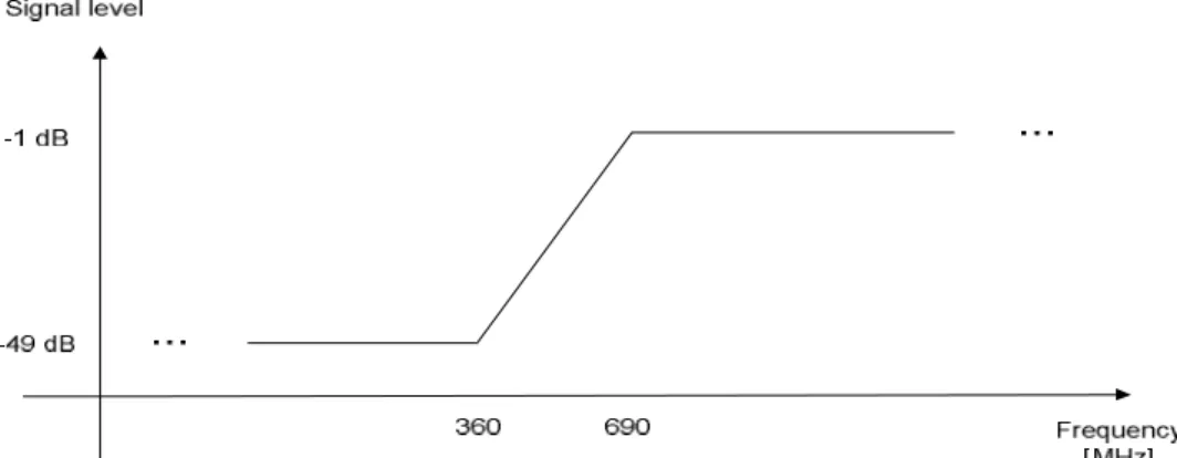
In this worst-case scenario, 80 dB of attenuation of the LO1 tone level relative to the signal is exceeded. It is inserted with an amplitude of -49.41 dB and a variable frequency dependent on the LTE band for filtering. The following subsection will first consist of a summary of the calculated specifications of the LO rejection filters and then a presentation of the actual filter circuits (those that meet the specifications).
Summary of Specifications and Filters Actually Projected
- Sub Band 1
- Sub Band 3
- Sub Band 1
- Sub Band 2
To reject the LO tone, the ideal filter response shown in Figure 4.9 can be used. To reject the LO tone, the ideal filter response shown in Figure 4.11 can be used. To reject the LO tone, the ideal filter response shown in Figure 4.13 can be used.
Comparisons between specifications and results
As for LO2, it always has a frequency 600 MHz lower than the center frequency of the signal. This is relevant for performing the calculations in section 4.3, which addresses the problem of SNR degradation in the upconverson block. This information is also very important to get an idea of the filter quality achieved by each filter.
Simulation range of Attenuation of the filters designed
Matlab and FPGA Simulations
- Single Run Matlab Simulation .1 OFDM Signal generation
- Analog Filters Simulation
- Matlab Simulation Results
- FPGA Simulation
- Multiple Run Matlab Simulation
You can see this in Figure 5.14, where there is a zoomed-in view of the signal spectra. You can see this in Figure 5.24, where there is a zoomed-in view of the signal spectrum. Note that the signal spectrum is clearly higher at lower frequencies.
Final Remarks
- Future Work
- Conclusions
There are some problems that may arise in the remaining studies to be carried out, to enable the development of the functional LTE filter discussed. Note that the transition bands of the functional filters of the system developed are relatively small compared to their cutoff frequencies. This is very beneficial, since the periodicity of the response is unlikely to hinder the quality of the achieved filtering.
Available: http://www.st-andrews.ac.uk/~www_pa/Scots_Guide/RadCom/part13/page1.html. 32] (September 2013), “Expanded Overview of the Spartan-3A Family”, Product Specifications, Xilinx [Online] Available: http://www.xilinx.com/support/documentation/data_sheets/ds706.pdf. 35] (September 2013) [Online] “Filter Design Toolbox User's Guide”, Mathworks, Version 2 (Chapter 1 – Filter Design Toolbox Overview and Chapter 10 – Using FDATool with filter design toolbox) [Online] Available: http://www .busim.ee.boun.edu.tr/~resources/fdq.pdf.
Appendix
- LTE Bands details
- Downlink LTE Band
- Uplink LTE Band
- Downlink LTE Band
- Uplink LTE Band
- Algorithm for SNR Degradation determination
- Single MosFET Mixer Analysis
- Tables of functional filters’ components
- Filter conversion to Microstrip line technology
- ADC - Some important specifications
- ADC – Types of Error
- Study of IIR filters as the FPGA Digital Filter
- Detailed Information of FIRs’ hardware implementation
A change in the slope is due to a change in the length of the quantization intervals (which would ideally be equal to q). The area of the ADC response where the DNL error is introduced is surrounded by a dashed red circle. The arrow in Figure a3.7 points toward the center of the step in the response furthest from the ideal ADC response.
Serial FIRs
In reality, INL errors are just the name for the accumulation of DNL errors. In other words, when thinking about a transition between code words, it is the maximum difference between the analog voltage that should trigger that transition and the one that actually does because of the accumulation of DNL errors. The higher its absolute value and closer to 1 (but less than 1), the more difficult it will be to realize the filter.
Transposed FIRs
Symmetric Systollic FIRs Mathematical analysis
Recursive Calculations For Filters’
Frequency Response Matlab Simulation
Analyzing figures a5.1 and a5.2, a solution was created to calculate the transfer function of a filter at each of the mentioned frequencies. Filter components are entered into matlab from right to left (figures a5.1 and a5.2), with the possibility of having any impedance equal to 0. This array is itself, an input to the software routine call that “ adds” components to the filter.
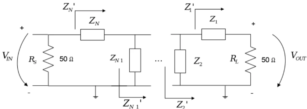
Impedances
IP3 Error after each mixing step
The IP3 error after the first mixing step consists of one 60 MHz bandwidth centered in 600 MHz. After the second downconversion step, the maximum IP3 error power density is now 250.08 dBW/Hz and the minimum signal power density is -109.33 dBW/Hz.