X-ray Study of Strain, Composition, Elastic energy and Atomic ordering in Ge islands on Si(001)
X-ray Study of Strain, Composition, Elastic
energy and Atomic ordering in Ge islands
on Si(001)
Ângelo Malachias de Souza
Thesis submitted to the UNIVERSIDADE FEDERAL DE MINAS
GERAIS as a partial requirement for obtaining the Ph.D. degree in
Physics.
Thesis supervisor: Prof. Dr. Rogério Magalhães Paniago (UFMG) Thesis co-supervisors: Dr. Gilberto Medeiros Ribeiro (LNLS)
Dr. Till Hartmut Metzger (ESRF – Grenoble)
Agradecimentos
−
Acknowledgements
−
Remerciements
Professor Rogério Paniago, pelo interesse sincero na minha formação como cientista. Durante todo o doutorado não me deparei com qualquer entrave ou obstáculo que, graças ao seu empenho, não tenha sido contornado. Sou grato pelos conselhos e discussões (científicos ou não).
Dr. Gilberto Medeiros Ribeiro, pelo extremo otimismo e espírito crítico, capazes de remover nossas análises e interpretações do lugar comum. Agradecer-lhe pelas amostras é um mero detalhe...
Dr. Hartmut Metzger for his warm hospitality during my stay in Grenoble, for the confidence and freedom he gave me, for the nice and positive atmosphere of his group and for being open towards many (unscheduled) scientific discussions.
Dr. Stefan Kycia, for the crucial improvements of the diffraction beamlines at LNLS that made this work possible and for sharing his experimental knowledge. I also have to thank his continuous support during many experiments.
Dr. Tobias Schülli, for the productive collaboration. Our interaction has been a continuous source of ideas, learning and motivation.
Dr. Václav Holý, for his interest and kindly advice in the interpretation of x-ray measurements.
Dr. David Cahill, Dr. Martin Schmidbauer, Dr. Oliver Schmidt and Dr. Mathieu Stoffel for their invaluable support with samples, ideas and criticisms.
Luiz Gustavo Cançado, pela ajuda com as medidas de Raman e análise dos resultados.
Agradeço aos colegas do Laboratório de Nanoscopia, Prof. Bernardo, Giselle, Bráulio, Elisângela, Lino, Ana Paula, Ivonete e Mariana, por, no convívio diário, me contagiar com seu bom humor (mesmo nos dias mais tensos).
Agradeço aos amigos do Departamento de Física da UFMG, Prof. Luiz Cury, Gustavo Sáfar, Daniel Elias, Letícia Coelho, Guilherme José e Antônio Francisco Neto por manterem um ambiente profissional agradável e acolhedor. Este agradecimento é extensivo a todos aqueles que comigo conviveram durante esses últimos quatro anos.
Sou grato a Marluce, Idalina e Júlio, pela extrema eficiência com que resolveram meus problemas burocráticos, tratando minha tradicional ansiedade com paciência infinita.
Je tiens a remercier Dr. Olivier Plantevin, Dr. Bruno Jean et Hamid Djazouli pour leur aide technique, leurs précieux conseils dans le domaine administratif, ainsi que pour leurs encouragements.
Dr. Peter Böescke for bringing successful, immediate and efficient solutions to all technical problems at beamline ID01. I also thank Dr. Cristian Mocuta for interesting scientific discussions and for his optimism.
Je remercie Mme Leila Van Yzendhorn pour m'avoir aidé à resoudre mes problèmes pratiques (surtout logement et documentation). Mes remerciements vont également à Mme Martine Cédile pour m'avoir appris, courageusement, un peu de français.
Agradeço aos amigos Ernesto Paiser (extensivo à Laura, Laurent e Sophie) e Ricardo Hino (também Natalie, Cecília, Emma e Lisa) pelos agradáveis momentos em família que compartilharam comigo em Grenoble.
Sou grato a Leide, Júlio, Daniela e Fabiano pelo apoio constante e pelas divertidas reuniões.
Agradeço profundamente à minha mãe pelo carinho e esforço dedicados a minha educação e crescimento moral. Ao meu pai devo agradecer por sempre me alegrar nas horas boas ou ruins e pelas nossas conversas de onde tirava uma incrível sabedoria prática. Não há um único dia em que não sinta a falta dos dois (espero ter crescido frente às expectativas deles...).
Sou muito grato a Marina por ter estado sempre ao meu lado nos momentos difíceis que enfrentamos, principalmente nos primeiros anos do doutorado.
Agradeço aos meus amigos Bruno Friche, Fred, Camilo, Léo π e Bruno Durão pelo estímulo e amizade.
Sou imensamente grato à Ângela Maria, João Calixto, Cláudia e Flávia pela constante ajuda e apoio.
Tia Ione, Tio Marcos, Juliana, Cristina, Mariza, Luís e Emerson por resgatarem minha alegria do convívio com a família, também pelo carinho e atenção.
Tia Dirce por estar por perto em todas as horas, com seu otimismo e senso prático.
Tia Gilda pelo carinho e incentivo.
Abstract
Resumo
CONTENTS
Abstract
Resumo
Introduction . . . 1
Chapter 1 – X-ray Scattering at Surfaces . . . 2
1.1 – Synchrotron radiation . . . 2
1.2 – Grazing-incidence diffraction . . . .
6
1.2.1 – Distorted-wave Born approximation . . . 9
1.3 – Form Factor . . . 12
1.4 – Atomic scattering factor and anomalous x-ray scattering . . . 15
1.4.1 – Anomalous (resonant) x-ray scattering . . . 16
1.5 – Structure factor . . . .20
1.5.1 – Long-range order parameter S . . . .23
Chapter 2 – Self-assembled Ge Islands on Si (001). . . 26
2.1 – Elastic properties of cubic crystals . . . 26
2.1.1 – Strain . . . 26
2.1.2 – Elastic energy
. . . 28
2.2 – Ge deposition on Si(001) . . . 30
2.3 – In-plane strain distribution . . . .
34
2.4 – Island strain mapping by angular scans. . . .36
2.5 – Evaluation of the Ge/Si concentration . . . .
39
2.6 – Strain relaxation and elastic energy . . . 41
Chapter 3 – 3-Dimensional Composition of Ge Domes . . . 50
3.1 – Lateral interdiffusion . . . 50
3.1.1 – Complete analysis on sample A (CVD). . . 52
3.1.2 – 3D composition analysis on sample B (MBE). . . 57
3.2 – Elastic energy maps . . . 60
3.3 – Discussion
. . . .63
Chapter 4 – Atomic Ordering in Ge Islands on Si (001) . . . 65
4.1 – Ge/Si atomic ordering in thin films . . . 65
4.2 – Sample characterization using Raman spectroscopy . . . .
70
4.3 – X-ray measurements in sample B . . . .
71
4.4 – Bragg-Williams order parameter of samples grown at different
temperatures . . . 81
4.5 – Discussion . . . .
85
Chapter 5 – Conclusion . . . 86
Chapter 6 – Síntese do trabalho em português . . .
88
6.1 – Introdução aos métodos experimentais . . . .
88
6.1.1 – Difração por incidência rasante . . . .88
6.1.2 – Espalhamento anômalo (ressonante) de raios-x . . . .
89
6.1.3 – Fator de estrutura e parâmetro de ordem S . . . .
91
6.2 – Composição e strain em ilhas de Ge:Si. . . .
93
6.2.1 – Crescimento de ilhas de Ge em Si(001). . . .93
6.2.2 – Avaliação da composição médianas ilhas de Ge:Si . . .
96
6.2.3 – Energia elástica média
. . . .98
6.2.5 – Mapeamento 3-D da energia elástica para domos. . . . 104
6.3 – Ordenamento atômico . . . .105
6.3.1 – Ordenamento atômico em filmes de Ge:Si . . . .
105
6.3.2 – Espectroscopia Raman e ordem de curto alcance
. . . .
106
6.3.3 – Análise de ordenamento para a amostra B
. . . .107
6.3.4 – Parâmetro de ordem S para a série de amostras. . . .
112
6.4 – Conclusões . . . 113
References . . . 115
List of publications (2002 - 2005) . . . 121
Introduction
Nanostructured materials have attracted the interest of basic and applied research during the last two decades. The eletronic response of one–dimensional and zero– dimensional systems such as self assembled semiconductor islands (quantum dots) and nanowires, fulerenes, carbon nanotubes and polymers strongly depend on their morphological, structural and chemical properties.
In this thesis the x-ray diffraction technique is employed to study the most relevant features of self-assembled Ge:Si(001) islands. Three-dimensional maps were obtained for the following parameters:
1) strain, that influences semiconductor band alignment and the quantum efficiency of nanostructures;
2) composition, that changes the confining profile (by changing the energy bandgap);
3) elastic energy, that may render an island ensemble stable, with a preferred shape and a fixed size distribution, directly related to the width of spectral and eletronic response of these materials;
4) atomic order, that can also affect the band alignment.
Chapter 1
X-ray Scattering at Surfaces
1.1 Synchrotron Radiation
Synchrotron facilities have become essential in many fields of science. There are
many advantages in using synchrotron radiation instead of conventional x-ray sources:
energy tunability, polarization, coherence and high brilliance. These properties lead to the
development of x-ray techniques such as scattering, spectroscopy, imaging and
time-resolved studies. A detailed introduction to synchrotron radiation can be found in
[AlsNielsen01] and [Michette01].
The measurements shown in this thesis were performed at the Brazilian National
Source LNLS (Laboratório Nacional de Luz Síncrotron), located in Campinas and at the
ESRF (European Synchrotron Radiation Facility), located in Grenoble (France). All
experiments described in this thesis profit from the tunability of the x-ray photon energy for
anomalous scattering and from the high brilliance of these facilities. Since this work is
based on the analysis of surface reflections and superstructure peaks the use of enhanced
brightness synchrotron sources was imperative. The emission spectra of ESRF and LNLS
Fig. 1.1: Schematic representation of synchrotron radiation spectral range. The bremsstrahlung curves for LNLS and ESRF bending magnets (BM) beamlines are represented by blue and red solid lines, respectively. The graph also shows the spectral response of an ESRF wiggler (W70 – green dashed line) and an undulator (U42 – purple solid line). Arrows indicate the typical photon energies used for selected x-ray techniques.
Two beamlines of the LNLS are dedicated to x-ray diffraction in single crystals:
XRD1 and XRD2. Both operate in an energy range between 4 and 12 KeV (wavelength
range between 3 and 1 Å). Their optics systems are essentially the same. A gold-coated
silicon mirror is used to remove high energy photons, focusing the white beam vertically. A
double crystal Si(111) sagital monochromator makes the horizontal focalization. XRD1
beamline is equipped with a 2+1 circle diffractometer. It consists of a theta-2theta vertical
measurements in different (and more complex) geometries such as reciprocal-space
mapping of asymmetric reflections.
At the ESRF all experiments were performed at the ID01 beamline, which is
equipped with an insertion device (undulator or wiggler, depending on the energy range) to
increase the photon flux. The optics hutch is equipped with two Si mirrors and a sagital
double crystal Si(111) monochromator. The intensity of the monochromatic beam at 8KeV
is approximately 106 times larger than a bending magnet beamline of LNLS. The ID01
beamline is equipped with a 4+2-circle diffractometer where four degrees of freedom are
used to sample positioning and two for the detector movement.
A schematic representation of the x-ray optic elements of XRD1/2 and ID01
beamlines is shown in fig. 1.2.
Fig. 1.2 - (a) Sketch of X-ray optical elements of XRD1/2 (LNLS) beamlines. (b) ID01 optics hutch scheme.
Fig. 1.3 shows the diffractometers of the three beamlines and their movements.
Fig. 1.3 – Diffractometers of (a) XDR1 and (b) XRD2 beamlines at LNLS and (c) ID01 beamline at ESRF. The x-ray path is indicated by the yellow line while diffractometer movements are represented by arrows.
(c)
structural parameters along this thesis. Section 1.2 is dedicated to atomic scattering factor
and its dependence on the x-ray photon energy. A brief introduction to the use of
anomalous (resonant) x-ray scattering to obtain chemical contrast is found in this section.
Form factor and structure factor calculations are shown in section 1.3 and 1.4, respectively.
Finally, in section 1.5 we discuss the x-ray technique which is employed here to investigate
structures on the near-surface region: Grazing Incidence Diffraction.
1.2 Atomic scattering factor and anomalous x-ray scattering
Essentially two types of interaction can occur when an x-ray photon falls on an
atom. The photon may be absorbed by the atom, with ejection of an electron or it can be
scattered. It is useful to start a description of these processes from the most simple case: the
elastic scattering of a photon by a single electron following the classical theory. If the
radiation is unpolarized the acceleration of the electron will be given by the force of the
electromagnetic field from the incident wave E0e–iωt acting on the particle that has charge q
and mass m: [Jackson99]
m e q m
t iω
=
= f E0
a . (1.1)
According to the electromagnetic theory an accelerated charge radiates. The
radiated energy is proportional to the square of the radiated field Erad. Then, Erad must
decrease as 1/R. Since the elementary scattering unity of an X-ray in an atom is the electron the field is proportional to its charge –e and to the acceleration a(t’) evaluated at a time t’=t–R/c earlier than the observation time t (the radiation propagates at a finite velocity
c). The electric field that results from this acceleration is given by:
( )
R c
' t ea
2 0
4πε − − = rad
E (1.2)
where the term 1/(4πε0c2) was included to make eq. 1.2 dimensionally correct. By using
( )
( )
ψ⎟⎟ ⎠ ⎞ ⎜⎜ ⎝ ⎛ πε − = ⇒ ψ − πε − − = ⎟⎠ ⎞ ⎜ ⎝ ⎛ ω cos R e mc e t , R cos e m e R c e t , R ikR c R i 2 0 2 2 0 4 4 in rad in rad E E E E
, (1.3)
where k=ω/c and Ein= E0e–iωt. The the position of the observer relatively to the acceleration direction is represented by the inclusion of the term cosψ. For ψ=π/2 the observer does not see any acceleration while for ψ=0 the full acceleration is observed. The prefactor of the spherical wave eikR/R is denoted by r0=(e2/4πε0mc2) and known as the classical electron radius [Jackson99, AlsNielsen01].
1.2.1 Atomic form factor
In the preceding pages the x-ray scattering was calculated considering one free
electron. However, in real atoms the electrons are spatially restricted to a small volume
around the nucleus. The atom is then viewed by x-rays as a charge cloud with a number
density ρ(r). The charge in a volume element dr at a position r is, then, given by –eρ(r)dr.
To evaluate the scattering amplitude one must weight the element contribution dr by the
phase factor eiq.r and integrate over dr. This leads to the form factor of one atom, which is
also known as the Q-dependent part of the atomic scattering factor:
( )
=
∫
⋅r
r
ρ
Qrd
e
)
(
f
0Q
i . (1.4)At Q = 0 the result of eq. 1.4 is the total number of electrons Z in the atom. One can
assume, for simplicity, that the charge density has spherical symmetry with the
hydrogen-like form
ρ = (e–2r/a )/(πa3) (1.5)
( )
[
]
dr Qr ) Qr ( sin e r a dr e e iqr e r a dr d sin e e r a f r a r iQr iQr r a r cos iQr r a r 2 2 1 1 2 1 2 1 Q 0 2 2 3 0 2 2 3 0 0 2 2 3 0∫
∫
∫
∫
∞ = − − ∞ = − π = θ θ ∞ = − π π = − π π = θ θ π π =. (1.6)
The integrand is independent of the azimutal angle φ so that the volume element becomes
2πr2sinθdθdr. In order to solve eq. 1.6 the term sin(qr) is written as the imaginary part of a
complex exponential. Then,
( )
{
}
Im{
re(
)
dr}
qa dr e re Im qa f r iQ a r r iQr a r
∫
∫
∞= − − ∞ = − = = 0 2 3 0 2 3 0 4 4Q (1.7)
that may be integrated by parts to yield the final result
( )
(
)
[
2]
20 2 1 1 Q Qa f +
= . (1.8)
The atomic form factor f0(Q) given by eq. 1.8 and the form factors of Si and Ge atoms are plotted in fig. 1.4. These results refer to isolated atoms with spherical symmetry.
In a real crystal this symmetry is modified by the lattice and also depends on the type of
atomic bond (i.e, covalent or ionic).
1.2.2 Anomalous (resonant) x-ray scattering
The simple treatment of the atomic scattering factor outlined above is based in the
assumptions that the x-ray wavelength is smaller than any absorption edge wavelengths in
the atoms. In case this condition is not satisfied dispersion corrections are necessary. These
corrections take into account the fact that electrons are found in bound states of an atom.
Although the quantitative calculation of such corrections can be performed only by using
quantum mechanics formalism it is still possible to use a classical model to understand their
physical meaning. Let the incident field be polarized along the x axis, with amplitude E0
and frequency ω, Ein=xE0e–iωt. The equation of a forced charge oscillator describes the
motion of the electron [Jackson99, AlsNielsen01]:
t i s e m e x x
x ω ⎟ −ω
⎠ ⎞ ⎜ ⎝ ⎛ − = = +
+γ 2 E0
f
& &
& . (1.9)
This equation has a velocity dependent damping termγx&that represents the dissipation of
the applied field and a resonant term with frequency ωs (usually much bigger than the γ).
Using a trial solution x(t)=x0e–iωt the amplitude x0 of the forced oscillator is given by:
(
γ)
1 E
2 2 0
0 ⎟ ω −ω − ω
⎠ ⎞ ⎜ ⎝ ⎛ − = i m e x s
. (1.10)
Similarly to equation 1.2 the radiated field is evaluated at the earlier time t’=t–R/c
( )
x(t R c)R c e t
,
R ⎟⎟ −
⎠ ⎞ ⎜⎜ ⎝ ⎛ πε − −
= &&
2 0 4
rad
E . (1.11)
Inserting &x&(t−R c)=−ω2x0e−iωtei(ωc)Rand x0 given by equation 1.11 leads to
( )
(
)
( )
(
)
⎟⎟ ⎠ ⎞ ⎜⎜ ⎝ ⎛ ω + ω − ω ω − = ⇒ ⎟⎟ ⎠ ⎞ ⎜⎜ ⎝ ⎛ ⎟⎟ ⎠ ⎞ ⎜⎜ ⎝ ⎛ πε ω − ω − ω ω= −ω
R e i r t , R R e e m c e i t , R ikR s ikR t i s γ E 4 γ 2 2 2 0 0 2 0 2 2 2 2 in rad rad E E E
. (1.12)
The amplitude of the outgoing wave (in units of –r0) is given by the atomic scattering
For frequencies that are larger than the resonant frequency (ω>>ωs) the electron can
be considered free and equation 1.12 change its form to 1.3. The expression for fs can be rearranged in the following way:
(
)
(
γ)
1(
γ)
γ 1 γ γ γ 2 2 2 2 2 2 2 2 2 2 2 ω + ω − ω ω + ≅ ω + ω − ω ω − ω + = ω + ω − ω ω + ω + ω − ω − ω = i i i i i i f s s s s s s s
s . (1.13)
The last term follows from the fact that γ is usually much lower than ωs. From eq. 1.13 the
dispersion correction χ(ω) (also known as dieletric susceptibility) can be written as
( )
(
)
γ 2 2 2 ω + ω − ω ω = + = ω χ i " if ' f s s ss , (1.14)
with real and imaginary parts given by
(
)
(
)
( )
(
2 2)
2( )
22 2 2 2 2 2 2 2 γ γ and
γ ω −ω + ω
ω ω = ω + ω − ω ω − ω ω = s s s s s s
s' f "
f . (1.15)
These dispersion corrections for the single oscillator model are shown in fig. 1.5 with
ωs=0.1 [Jackson99].
Fig. 1.5 – Real fs’ and imaginary fs” parts of the dispersion corrections as a function of the ratio between the
driving frequency ω and the resonant frequency ωs.
In order to calculate the dispertion corrections for a real atom one must consider
formalism. This theoretical description is usually based on self-consistent equations that
describes an atom as a multi-electron system and will not be presented here.
The theoretical values of χ(ω) can be obtained only with a very precise knowledge of ωs and γ (there is no straightforward way to measure γ). However, the casuality principle
of electrodynamics can be employed to derive relations between real and imaginary parts of
χ(ω). These relations are known as the Kramers-Kronig dispertion relations. Since f’ and f”
are the real and imaginary parts of χ(ω) these relations can be written as [Jackson99]:
( )
∫
∞( )
( )
∫
∞( )
ω ω − ω ω − = ω ω ω − ω ω ω = ω0 2 2
0 2 2 and ' d '
' ' f " f ' d ' ' " f ' '
f . (1.16)
The first equation can be used to estimate f’ if f” is known from near-edge absorption
measurements. However, the integrals of equation 1.16 requires measurements from ω = 0 until ω = ∞ that are not feasible. Alternatively, it is possible to use tabulated values of f”
based on self-consistent theoretical calculations for multi-electron systems. These values,
which exist in a wide frequency range, can be combined with high resolution frequency
measurements close to the atomic absorption edges.
A program to perform the integration of the first equation 1.16 was made by Dr.
Tobias Schülli and is available on internet (http://www.schuelli.com/physics/kkpage.html).
To use this computer routine one must measure the x-ray absorption at the vicinity of the
absorption edge of interest. This is usually done by scanning the x-ray energy of the
incident beam while it is pointed out to a sample that contains the atomic specie of interest.
Tabulated values of f” are replaced by the re-normaized experimental intensity in the energy range which was measured and used as input to calculate f’. Fig. 1.6(a) shows
theoretical values for f’ and f” close to the Ge-K edge (E = 11103.1 eV). The set of
measured absorption data is pasted on top of the f” values – fig. 1.6(b) – and the
Fig. 1.6 – (a) Theoretical and (b) measured values for f” close to te Ge K absorption edge. Values of f’ are obtained by the first equation (1.16). The Id01 Si (111) monochromator used here has 1eV energy resolution. These corrections change the non-resonant Ge atomic form factor shown in fig. 1.4(c).
The scattering factor of an atom is, then, given by [AlsNielsen01, Warren69]:
( )
f'( )
E f"( )
E ff = 0 Q + + , (1.17)
where the photon energy E replaces the frequency dependence of f’ and f”. The first term, given by eq. 1.4, is proportional to the number of electrons of an atom and decreases for
high momentum transfer Q (higher scattering angles). By tuning the x-ray photon energy
one can change the values of f’ and f” and perform chemically sensitive experiments. Both Q and energy dependence effects were recentlly explored by Schülli et. al. [Schulli03a] to
1.3 Form factor of a small crystal
In section 1.2.1 the atomic form factor was calculated assuming a spherical electron cloud
surrounding the atom. For a general case, an object with arbitrary shape and homogeneous
charge density ρ will have a form factor Sobj given by the integral
∫
⋅=
ρ
(
r
)
e
iqrd
r
S
objθ
, (1.18)where θ(r) is a step function which has value 1 inside the object. The general form of
equation 1.18 holds for any continuous charge distribution.
A crystal can be imagined as a regularly repeated atomic arrangement and form
factors for the most simple crystal shapes can be calculated analytically1. All objects
studied in this work can be seen as stacks of 2D crystal layers. If the object has a four-fold
symmetry, the form factor can be calculated as a stack of square crystals. A square with N2
atoms with sides oriented along the qa and qr direction and lattice parameter d will scatter with intensity given by2:
(
)
20
4
( )
( )
i i
I
I
e
x dx
e
y dy
N
σ
σ
⋅ ⋅
=
∫
q xr⋅
∫
q yr. (1.19)
The atomic positions are denoted as
1 1
0 0
( ) ( ) and ( ) ( )
N N
j g
x f x jd y f y gd
σ − δ σ − δ
= =
=
∑
− =∑
−and the atomic scattering factor of each atom is given by f. Hence, using f = 1 for simplicity, the scattered intensity of one square-shaped atomic layer can be written as
( )
( )
2 1 1 0 4 0 0 2 1 1 0 4 0 0 ( ) ( ) a r N N i i j gN j N g
iq d iq d
j g
I
I e x jd dx e y gd dy
N
I
I e e
N δ δ ∞ ∞ − − ⋅ ⋅ = −∞ = −∞ − − = = ⎛ ⎞ = ⎜ − ⋅ − ⎟ ⎝ ⎠ ⎛ ⎞ ⇒ = ⎜ ⋅ ⎟ ⎝ ⎠
∑
∫
∑
∫
∑
∑
ar q y
q x
. (1.20)
The summations of the last equation have the form of geometric progressions for which the
2 4 0 1 1 1 1 − − ⋅ − −
= iqiqNdd iqiqNdd
a a r r e e e e N I
I . (1.21)
To obtain the scattering of an island that consists of a stack of square layers one
must sum over the contributions of layers with different side lengths L = Nd and/or lattice parameters d. The result for the complete structure is obtained performing a sum over the heights hj of the atomic layers with respect to the substrate [Malachias01]
2 1 2 4 0 1 1 1
∑
= − − ⋅ − = M j h iq q id q d iN a q iL z r a j z r j r j j a j e e e idq e M N I ) q , q , q (I . (1.22)
For fixed qr and qz eq. 1.22 can be simplified into [Warren69]
(
)
( )
2 2 0 2 a a a q sin q L sin L I ) q (I = . (1.23)
The form factor of a disc with constant charge density is very useful for structures
with radial symmetry. In this case Sdisc is given by the integral in cylindrical coordinates
[Kegel99]
( )
∫ ∫
π ⋅∫ ∫
π ϕϕ =
ϕ
= R i R iqrcos
dr rd e d rd e r 0 2 0 0 2 0 disc
S q qr r . (1.24)
Similarly to eq. 1.22 a stack of discs will scatter with intensity given by
2 1 0 2 0 4 2 2
0
∑ ∫ ∫
= π ϕ ⎥⎦ ⎤ ⎢⎣ ⎡ ϕ π = M j h iq R cos r iq z r a j z
r rd dr e
e R M I ) q , q , q (
I . (1.25)
1.4 Structure factor
The scattering of crystals with simple geometries can be understood by the results of
the preceding sections. However, the scattered intensity for a real crystal depends on the
symmetry of the atoms inside the crystal unit cells and is proportional to the structure factor
F. Atomic positions are represented by the vector rn = xna1 + yna2 + zna3.
We are interested in the value of F for an hkl-reflection when the Bragg’s law is
vector Hhkl is given by Hhkl= hb1 + kb2 + lb3 in terms of the reciprocal vectors b1 b2 b3. The structure factor for a Bragg reflection is [Warren69]
( )( )
∑
( )( )∑
( )∑
π λ ⋅=
π + + ⋅ + +=
π + +=
n lz ky hx i n n z y x l k h i n n / i n hkl n n n n nn
f
e
e
f
e
f
2 2 2F
q0rn b1 b2 b3 a1 a2 a3. (1.26)
If F = 0 for a given hkl reflection no scattered intensity of this reflection is also zero.
All materials studied in this work have diamond-like unit cells. It is easier to obtain
the diamond structure factor starting from a face-centered (FCC) cubic lattice. The basis of
a FCC unit cell consists of four atoms located in the coordinates (xn, yn, zn), (xn+½, yn+½,
zn), (xn+½, yn, zn+½) and (xn, yn+½, zn+½). Each unit cell with n atoms has (n/4) atomic groups that scatter with the same structure factor. Performing a sum over a 4-atoms group
leads to
[
+
π ++
π ++
π +]
∑
π + +=
4 21
F
n ) lz ky hx ( i n ) l k ( i ) l h ( i ) k h ( i hkl n n ne
f
e
e
e
. (1.27)If m is an integer, eπim = (-1)m, and hence the first factor takes the value 4 if hkl are all odd or all even and the value zero if hkl are mixed. Hence,
∑
π + + = 4 2 4 F n ) lz ky hx ( i n hkl n n n ef (hkl) unmixed and Fhkl =0 (hkl) mixed. (1.28)
The diamond (Si or Ge) structure, shown in fig. 1.7, consists of two FCC lattices shifted by
¼ in all directions. The Si (Ge) atoms in these two sub-lattices are located in the
coordinates ( ) ½ ½ 0 ½ 0 ½ 0 ½ ½ 0 0 0
Si1 → ( )
¾ ¾ ¼ ¾ ¼ ¾ ¼ ¾ ¾ ¼ ¼ ¼
Using the first equation 1.28 with the positions 0 0 0 for the Si(1) sub-lattice and ¼ ¼ ¼ for
Si(2) the structure factor can be written as
[
( i/ )(h k l)]
SiSi
hkl
f
f
e
+ + π
+
=
24
F
, for (hkl) unmixed. (1.29)Since the scattered intensity is proportional to the square of the structure factor, i.e.,
I∝ F2hkl=FhklF*hkl, then:
[
] [
]
⎥⎦ ⎤ ⎢⎣
⎡ + π + +
=
+ ⋅ +
= π + + − π + +
) l k h ( cos f f e f f e f f Si Si ) l k h )( / i ( Si Si ) l k h )( / i ( Si Si hkl 2 2 2 16 16 F 2 2 2 2 2
. (1.30)
Table 1 shows the scattered intensities of a Si (diamond) structure for different
reflections (n is an integer number).
Reflection Intensity
h+k+l = 4n Fhkl2 = 16(2fSi)2
hkl odd Fhkl2 = 16(2fSi2)
hkl mixed Fhkl2 = 0
h+k+l = (2n+1)2 Fhkl2 = 0
Table 1 – Structure factors of a Si crystal for different reflections.
Key examples of the reflections of the first type are (2 2 0), (4 0 0) and (6 2 0). The
second type of reflection includes (1 1 1), (3 3 3) and (3 1 5). Reflections with mixed index
are known as lattice-forbidden since the primary lattice (in this case FCC) determines their
null structure factor. Reflections of the fourth kind (h+k+l = 4n+2) are called basis-forbidden due to their dependence on the sub-lattice (or basis).
In the case where a second type of atom (Ge) is introduced in the Si lattice different
reflections can appear. For instance, a Si-Ge zincblend structure as shown in fig. 1.8. Two
sub-lattices with Si and Ge atoms located in the following positions:
Fig. 1.8 – SiGe zincblend (pseudodiamond) unit cell. Si atoms are represented in green while Ge atoms appear in orange.
The fourth kind of reflection of table 1 presents a non-zero structure factor for the
zincblend ordered configuration. The new value of F2 will be given by [Warren69]
Fhkl2 = 16(fGe – fSi)2 for h+k+l = (2n+1)2. (1.31)
This kind of reflection that depends on the possibility of ordering of the alloy is
known as superstructure reflection. An ordered alloy consists of sub-units that are periodic
along the crystal. The arrangement of alternate Si and Ge atoms in the [1 0 0] direction
(such as …Si-Ge-Si-Ge-Si-Ge-Si…) will give rise to a (2 0 0) reflection. If the repetition
unit consists of four atoms with the arrangement (…Si-Si-Si-Ge-Si-Si-Si-Ge-Si-Si-Si-Ge...)
the (1 0 0) reflection should be measured as a superstructure reflection.
1.4.1 Long-range order and order parameter S
Considering a binary crystal with two kinds of atoms – Si and Ge – the ordered
structure has two kinds of positions which will be designated α and γ. For a completely
ordered alloy with ideal stoichiometric composition the α-sites are all occupied by Ge
atoms and the γ-sites by Si atoms. In this case the sample composition is the sum of the
Some useful parameters for the site occupancies can be defined. Let us call rα and rγ
the fraction of α-sites and γ-sites occupied by the right atoms. In the other hand wα and wγ
are the fraction of α and γ sites occupied by the wrong atom [Warren69]. These parameters
are related by rα + wα = 1 and rγ + wγ = 1. There is also an additional condition that the
fraction of sites occupied by Si atoms must be equal to the fraction of Si atoms (the same is
valid for Ge). This can be expressed by:
mαrα + mγwγ = nGe , mγrγ + mαwα = nSi. (1.32)
A convenient notation for nonstoichiometric compositions is the Bragg and
Williams order parameter S. The definition of S has to be linearly proportional to (rα + rγ)
with S = 0 for a completely random arrangement and S = 1 for rα = rγ = 1 and
stoichiometric compotision. Expressing the linear dependence by S = a + b(rα + rγ), the first
condition (S = 0) gives 0 = a + b since a random alloy has half of its α and γ atoms in the
right sites and half in wrong sites. The second condition (S = 1) gives 1 = a + 2b since all
atoms are in their right sites. Eliminating the constants a and b the long-range order
parameter is expressed as [Warren69]:
S = rα + rγ – 1= rα – wγ = rγ – wα. (1.33)
With this definition for S the structure factors F for the superstructure reflections are
proportional to S and hence a general parameter S2 is obtained from the experiment. The
structure factor for a partially ordered alloy can be obtained by summing over all atomic
positions in the unit cell. Since there are two different kinds of atomic sites (α and γ) the
total sum of eq. 1.26 can be divided into a sum over the α positions and a sum over the γ
positions using the average scattering factor of each kind of site:
(
)
( )∑
(
)
( )∑
γ
+ + π γ
γ α
+ + π α
α + + +
= n n n i hxn kyn lzn
Ge Si
lz ky hx i Si
Ge f e f f e
f
F r w 2 r w 2 .(1.34)
For the case of the pseudodiamond structure of fig. 1.8 the positions of Ge and Si
(
)
( )(
)
( ) ( )(
)
(
)
(
)
(
)
⎭ ⎬ ⎫ ⎩ ⎨ ⎧ + ⎥ ⎦ ⎤ ⎢ ⎣ ⎡ ⎟ ⎠ ⎞ ⎜ ⎝⎛π⋅ + + + ⎟ ⎠ ⎞ ⎜ ⎝
⎛π⋅ + + + ⎭ ⎬ ⎫ ⎩ ⎨ ⎧ ⎥ ⎦ ⎤ ⎢ ⎣ ⎡ ⎟ ⎠ ⎞ ⎜ ⎝
⎛π⋅ + + + ⎟ ⎠ ⎞ ⎜ ⎝
⎛π⋅ + + + = ⎭ ⎬ ⎫ ⎩ ⎨ ⎧ + + ⎭ ⎬ ⎫ ⎩ ⎨ ⎧ + = + + + = γ α α γ + + π γ α + + π α γ γ γ + + π α α w 2 2 r 2 2 w r w r w r w r w r 2 2 2 l k h isin l k h cos f l k h isin l k h cos f e f e f f f e f f F Ge Si l k h i Ge l k h i Si Ge Si l k h i Si Ge
. (1.35)
The structure factor of the allowed reflection (400) will be given by
F(400) = fSi {rγ + wα} + fGe {rα + wγ}= 2(fSinSi + fGenGe); (1.36)
where the fraction of α-sites and γ-sites in eq. 1.32 are mα= ½ and mγ= ½.
For the (200) superstructure reflection the structure factor of eq. 1.31 is
re-calculated as
F(200) = fSi {rγ – wα} + fGe {–rα + wγ} = S(fSi – fGe), (1.37)
Where S was obtained using eq. 1.33.
Then, the integrated intensity of the (200) reflection is proportional to
I(200) = cV200S2(fGe – fSi)2, (1.38)
where V200 is the volume of the region at the bragg condition and all scattering constants
are represented by c. The integrated intensity of the (400) reflection can be written as
I(400) = c4V400(fGenGe + fSinSi)2, (1.39)
The order parameter S can be experimentally obtained by comparing the ratio of the
measured intensities. Assuming that the intensities were measured in a region of reciprocal
space with equal volume (V400 = V200) the ratio between intensities will be given by:
(
)
(
)
22 2 400 200 n n 4 S I I Si Si Ge Ge Si Ge f f f f + −
= . (1.40)
Hence,
(
)
(
Ge Si)
Si Si Ge Ge f f f f − +
= 2 n n
I I S
400
Although the results of eqs. 1.36 – 1.41 were calculated for a zincblend structure
they are valid for any system with two kinds of sites and two kinds of atoms with nGe= nSi =
0.5 and mα(Ge) = mγ(Si) = 0.5.
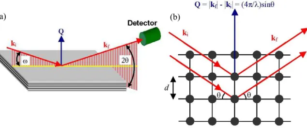
1.5 Grazing-Incidence Diffraction
In a typical set-up for x-ray diffraction the incident and exit beams are coplanar.
According to Bragg’s condition, x-rays are reflected from atomic planes with a spacing d
when the path length difference of the x-ray wave into the crystal is an integer (n) multiple
of the wavelength. This leads to the well-known Bragg’s law: nλ = 2dsinθ. In fig. 1.9 a
sketch of a coplanar x-ray diffraction geometry is shown, where ω is the incident angle and
the diffracted intensity is measured by the detector under an angle 2θ relative to the
incident beam. In this geometry the lattice parameter perpendicular to the surface plane can
be measured. Since the wave vectors of the incident and scattered beams are given by |ki| =
|kf| = k = 2π/λ the x-ray momentum transfer in calculated as Q = kf – ki.
Fig. 1.9 – (a) Geometry used for coplanar x-ray diffraction. (b) Sketch of Bragg’s law in reciprocal space. The usual formula nλ = 2dsinθ can be obtained assuming |Q| = n2π/d.
Fig. 1.9(b) shows a sketch of Bragg’s law in a coplanar symmetric geometry where
the incident and exit angle with respect to the crystal surface are the same.
If one needs to use x-rays as a surface sensitive probe a non-coplanar geometry
must be employed. The technique that combines surface sensitivity and diffraction from
crystal planes perpendicular to the sample surface is known as Grazing-Incidence
Diffraction (GID). It profits from the total external reflection of x-rays at low incident
angles [Dosch92].
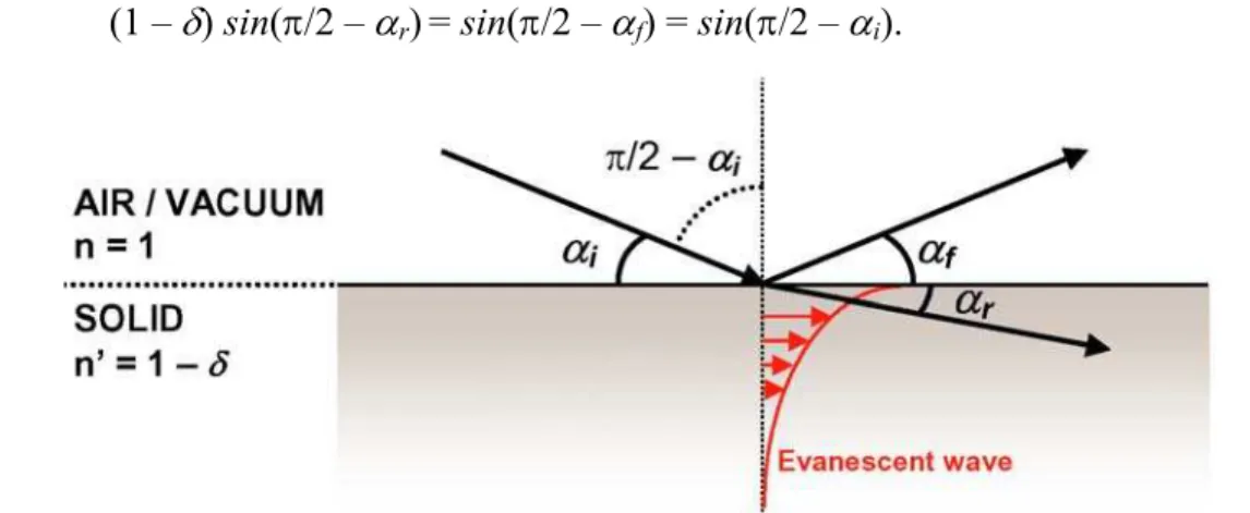
The refractive index of x-rays is generally described by n = 1 – δ + iβ, where δ is
the dispersion correction constant and β is the absorption correction [Vineyard82,
Dosch92]. For typical wavelengths and common solid materials these constants have values
of the order of 10-5, generating a refractive index slightly smaller than 1.
Fig. 1.10 shows schematically Snell’s law that relates the incident grazing angle αi to the refracted and reflected grazing angles αr and αf. Since the refraction index outside the solid is equals to unity the following relationship is valid (here we neglect the constant
β):
(1 – δ) sin(π/2 – αr)= sin(π/2 – αf) = sin(π/2 – αi). (1.42)
Fig. 1.10 – Representation of Snell’s law for x-ray reflection/refraction in solids.
Eq. 1.42 can be re-written as
(1 – δ) cos(αr) = cos(αf) = cos(αi). (1.43)
X-rays undergo total external reflection for αr = 0 that implies cos(αr) = 1. In this case, using eq. 1.43, the incident critical angle αc is given by
(1 – δ) = cos(αc) ≈ 1 – αc2/2. (1.44)
(x r zsin r) i i
e
E
e
E
⋅=
⋅ α + α=
cos 0 0 k x kE
, (1.45)where x is the direction along the interface and z is the normal direction. From eq. 1.43 one
can write (1 – δ) cos(αr)= cos(αi) and
cos(αr)= cos(αi)/(1 – δ). (1.46)
Using sin2(αr) = 1 – cos2(αr) and eq. 1.46 one gets
2 2
cos cos
sin 1 1.
1 1 i i r i α α α δ δ ⎛ ⎞ ⎛ ⎞ = −⎜ ⎟ = ⎜ ⎟ − − −
⎝ ⎠ ⎝ ⎠ (1.47)
With the results of eq. 1.46 and 1.47, eq. 1.45 becomes
1 2 2 cos cos 1 1 1 0 i i
k z ik x
E e
e
α α δ δ ⎡ ⎛ ⎞ ⎤ ⎛ ⎞ − ⎢ −⎜ ⎟ ⎥ ⎜ ⎟ − ⎝ ⎠ ⎢ ⎥ − ⎣ ⎦ ⎝ ⎠
=
E
. (1.48)Eq. 1.48 describes an evanescent wave that propagates parallel to the solid surface
with an exponencial damping in its amplitude across the interface. In this case the x-ray
evanescent wave has a limited penetration depth in the sample. The x-ray penetration depth
has the form [Dosch92]:
l L ⋅ = π λ 2 (1.49) with
(
) (
[
)
]
12 2 1 2 2 2 2 2 1 4 2 sen sen 2 2 ⎭ ⎬ ⎫ ⎩ ⎨ ⎧ − + − += − δ αi αi δ β
l . (1.50)
The minimum scattering depth is about 50Å for the asymptotic value αi = 0.
In the experimental setup for GID the sample is illuminated by the x-ray beam at a
shallow incident angle αi (αi < αc). The crystal is rotated around the surface normally until a particular lattice plane lying perpendicularly to the surface fulfills the Bragg condition. A
position sensitive detector (PSD) oriented perpendicular to the sample surface is used to
collect all wavevectors kf in the vertical (z) direction [Metzger98, Malachias02].
A relative momentum transfer coordinate system (radial-angular) is used for the
measurements. The radial momentum transfer qr defines the distance from the origin of
reciprocal space. The angular momentum transfer qa is related the deviation ∆ω from the
from the qr-qa plane. A schematic representation of the GID geometry and momentum
transfer vectors is shown in fig. 1.11 [Kegel99, Malachias02].
Fig. 1.11 – Grazing-Incidence Diffraction geometry. The x-ray beams are represented in red while the momentum transfer vectors were drawn in blue. The radial (qr), angular (qa) and vertical (qz) components of
momentum transfer are shown in detail on the right.
In this case, using |ki| = |kf| = k0 = 2π/λ the momentum transfer components are
given by:
( )
( )
(
sin sin)
. q sin sin q sin q f i z a r α + α λ π = ω ∆ θ λ π = θ λ π = 2 2 2 4 2 2 4. (1.51)
Reciprocal space scans in the directions of these three components have different meanings.
Scans in the qr direction are sensitive to variations in the crystal lattice parameter d (strain).
These scans, called radial scans, cross the path that points from the reciprocal space origin to the Bragg reflection position. Scanning the angular component qa one can probe the size
and shape of a region with a fixed lattice parameter. The direction of these so called
angular scans is, by definition, perpendicular to qr. Finally, scans along qz can be used to obtain vertical information of the crystalline structure.
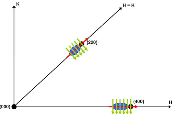
Figure 1.12 shows a sketch of the reciprocal space H-K plane and the directions of
both radial and angular scans. Experimental examples will be given in chapter 2 with a
Fig. 1.12 – Schematic representation of radial (qr) and angular (qa) scans in the reciprocal space H-K plane.
The reciprocal space points of a reference lattice and a strained lattice were represented in black and blue, respectively. Radial scans, represented by red arrows, cross the path along the line that connects a Bragg reflection position to the origin of the reciprocal space. Angular scans, shown in green, are perpendicular to the radial direction.
1.5.1 Distorted-Wave Born Approximation
The propagation of an electromagnetic plane wave in a medium with index of
refraction n is described by the homogeneous Helmholtz equation [Jackson99]:
0
2
2 =
+ ×
∇ ×
∇ E(r) k n E(r) , (1.52)
with k = 2π/λ and n = 1 – δ + iβ.
In order to model the scattering from a crystal with free-stading islands at the
surface one must use the Distorted-Wave Born Approximation (DWBA) [Rauscher99]. In
the DWBA the index of refraction (n2) of equation 1.52 is replaced by n2(r)= n02(z) + (1–
nisl2)Θisl(r). The substrate has a refraction index n02(z) equals to unity for z > 0 (vacuum)
and a constant value ns for the substrate (z < 0). Inside the islands the index of refraction is
corrected by the term nisl. Θisl(r) is a step function equals to the unity inside islands and
(
)
2 2 2 2
0 0 0
( ) ( ) ( ) 1 isl isl( ) ( )
E r k n z E r k n E
∇×∇× + = − − Θ r r . (1.53)
The solution of equation 1.53 is given by [Rauscher99]
(
|| ||)
[
(
z z)
F(
z z)
]
f expi expik r R exp ik r
E = k ⋅r ⋅ ⋅ + − ⋅ (z > 0) (1.54)
for the reflected/incident wave and
(
|| ||)
[
F(
z z)
]
f k r
~ i exp T i exp
E = k ⋅r ⋅ ⋅ (z < 0) (1.55)
for the transmitted wave. RF and TF are the Fresnel reflectivity and transmission
coefficients, respectively. The wave vector vertical component (for z < 0) inside the
substrate (where the index of refraction is ns) is represented by k~z. The wave vector breaks
down into its components k|| and kz, parallel and perpendicular to the surface.
The scattered wave amplitude is obtained treating the islands as a first order
perturbation [Rauscher99]
∫
≥ ⋅ Θ − π − − = 0 3 0 0 2 2 0 4 1 z i isl f i islsct E ( ', ) ( ' )E ( ', )d r'
r e ) n ( k ) (
E r r k r r k
r k
. (1.56)
Since the scattering comes solely from the islands (z > 0) E0 can be replaced by equation 1.54. This equation has two terms: the first is related to the scattered eletric field
and the second to the reflected part of the outgoing wave.
The scattered amplitude can be understood as a sum of integrals over all islands,
with the form
(
)
3 || ||(
)
||
,
'
( ')
i f z z
i i k k z
i f
isl
k
zk
zd r e
isl− ⋅ − ± ±
Θ
± ±
=
∫
q rΘ
r
r
%
, (1.57)where Θ~isl is the Fourier transform of Θisl. Each sign combination of the scattered (kf) and
incident (ki) wave vectors can be associated to a different scattering process according to fig. 1.13. Writing eq. 1.56 as functions of Fourier transforms of eq. 1.57 the scattered
amplitude [Rauscher99, Kegel01]
(
)
(
)
[
Θ + Θ − +π −
−
= isl ik⋅r isl || z f isl || z
sct , p
~ R q , ~ r e ) n ( k ) (
E r q q
4 1 2 2 0 r r
with pz = kzf + kzi. Rf and Ri are the reflectivities of the incident and scattered waves,
respectively. Each term of eq. 1.66 is related to one of the scattering processes shown
below.
Fig. 1.13 – Four scattering processes according to equation 1.66. Process 1 is a direct scattering from an island. Process 2 includes a substrate reflection after scattering. In (3) the beam is reflected by the substrate and then scattered by the island. Process 4 combines two reflections with one scattering event.
The differential cross section is then given by [Rauscher99]
( )
(
)
2 2 2 2 4 0 2 2 4 1 f z i z || islsct S ,k ,k
n k E r d d q π − = = Ω σ
, (1.59)
where S is the form factor of the four scattering events
(
)
[
isl(
|| z)
f isl(
|| z)
i isl(
|| z)
i f isl(
|| z)
]
fz i z
|| ,q
~ R R p , ~ R p , ~ R q , ~ k , k ,
Sq = Θ q + Θ q − + Θ q + Θ q . (1.60)
The scattered intensity (Isct∝ S*S) is obtained by integrating the cross section of eq. 1.59 in
the solid angle ∆Ω defined by the detector [AlsNielsen01]
( )
∆Ω∫
(
)
Ω π− φ
= S ,k ,k d
n k
Isct isl2 || iz zf 2 2 2 4 0 4 1
q , (1.61)
where φ is the photon flux defined by φ = I/A. I is the intensity of the incident x-ray beam
and A is the sample area. The definitions of cross section and scattered intensity used here
Therefore, x-ray scattering from free-standing islands can be modeled by four
different Fourier transforms of the islands. In principle, the ideal situation is when the last 3
terms are not as important as the first one. In this case, the internal structure of these islands
can be modeled by a single Fourier transform and the analysis of the data is considerably
simpler. This can be obtained by tuning the incident and exit angles such that Ri and Rf are
much smaller than one (using αi close to αc). The determination of the island shape and
composition becomes reasonably straightforward by modeling the structure and form
Chapter 2
Self-assembled Ge islands on Si(001)
2.1 Elastic properties of cubic crystals
2.1.1 Strain
The crystal lattice can be distorted due to externally imposed constraints on the
dimensions of the crystalline unit cell. These constraints arise because unit cells with an
“ideal” size are embedded in a macroscopic lattice which has its own (and different)
average unit cell dimension. Conceptually the externally imposed distortions can be
decomposed into a volumetric and a distortional component [Landau59].
The volumetric component comes when alloys are grown in bulk form, when
epitaxial films are grown on a lattice-matched substrate or when a hydrostatic pressure is
applied to a crystal. The distortional component comes about when epitaxial films are
coherently grown on a lattice-mismatched substrate. Suppose, for example, that the
substrate is a single unstrained Si1-xGex alloy crystal (bulk) whose Ge composition is x and
whose mean lattice parameter aSiGe(sub) is a weighted average (Vegard’s law) of the two
endpoint lattice parameters, aSiGe(sub) = (1 – x)aSi + xaGe.
If an epitaxial Si1-yGey film is grown on top of the Si1-xGex substrate then its lattice
the Ge composition y of the epitaxial film. This means that aSiGe(epi)||= aSiGe(sub) = (1 – x)aSi
+ xaGe.
There will be a parallel strain ε(epi)|| in the film given by [Tsao93]:
ε(epi)|| = 2(a(epi)|| – a(epi)unstr)/(a(epi)|| + a(epi)unstr), (2.1)
where a(epi)unstr = (1 – y)aSi + yaGe is the equilibrium (unstrained) lattice parameter of the
epitaxial film.
However, the lattice parameter perpendicular to the interface will change to
approximately keep the unit cell volume constant. If the film is locked to a substrate with
smaller parallel lattice parameter, the vertical dimension of the epitaxial film unit cell will
increase; if the substrate parallel lattice parameter is larger, the vertical dimension of the
unit cell of the epitaxial film will decrease.
A quantitative description of the volumetric and distortional components of
externally imposed strains can be done writing the generalized Hooke’s law for cubic
crystals [Landau59, Tsao93]:
⎟ ⎟ ⎟ ⎟ ⎟ ⎟ ⎟ ⎟ ⎠ ⎞ ⎜ ⎜ ⎜ ⎜ ⎜ ⎜ ⎜ ⎜ ⎝ ⎛ ⎟ ⎟ ⎟ ⎟ ⎟ ⎟ ⎟ ⎟ ⎠ ⎞ ⎜ ⎜ ⎜ ⎜ ⎜ ⎜ ⎜ ⎜ ⎝ ⎛ = ⎟ ⎟ ⎟ ⎟ ⎟ ⎟ ⎟ ⎟ ⎠ ⎞ ⎜ ⎜ ⎜ ⎜ ⎜ ⎜ ⎜ ⎜ ⎝ ⎛ zx yz xy z y x zx yz xy z y x C C C C C C C C C C C C γ γ γ ε ε ε τ τ τ σ σ σ 44 44 44 11 12 12 12 11 12 12 12 11 0 0 0 0 0 0 0 0 0 0 0 0 0 0 0 0 0 0 0 0 0 0 0 0
, (2.2)
where the εi’s and σi’s are the normal strains and stresses and the γi’s and τi’s are the shear
strains and stresses, respectively.
For an epitaxial film and substrate that are oriented along the <100> cubic
symmetry directions eq. 2.2 is reduced to
⎟⎟ ⎠ ⎞ ⎜⎜ ⎝ ⎛ ε ε ⎟⎟ ⎠ ⎞ ⎜⎜ ⎝ ⎛ + = ⎟⎟ ⎠ ⎞ ⎜⎜ ⎝ ⎛ σ σ ⊥ ⊥ epi || epi epi || epi C C C C C 11 12 12 12 11
2 . (2.3)
In the case of an epitaxial film with a free surface (e.g. uncapped films and/or islands) the
perpendicular stress vanishes, hence
The perpendicular strain and lattice parameter of the film will be given, respectively, by: || epi || epi epi C C ε ν − ν − = ε − = ε ⊥ 1 2 2 11 12 (2.5)
and .
2 1 2 1 ) ( ⊥ ⊥ ⊥ − + = epi epi unstr epi epi a a ε ε (2.6)
In eq. 2.5 ν is the Poisson’s ratio, defined as the negative of the ratio between lateral and
longitudinal strain constants under uniaxial longitudinal stress (ν = C12/[C11+C12])
[LandoltBornstein82]. The term that multiplies εepi|| in eq. 2.5 is the “equivalent” Poisson’s
ratio for a biaxial strain.
2.1.2 Elastic energy
To calculate the strain energy in a coherent epitaxial film it is useful to write the
generalized Hooke’s law, given by eq. 2.2, in terms of the Poisson’s ratio ν and the shear
modulus µ. µ is defined as the ratio between the applied shear stress and shear strain under
pure shear. Inverting eq. 2.2 one obtains [Tsao93]
⎟ ⎟ ⎟ ⎠ ⎞ ⎜ ⎜ ⎜ ⎝ ⎛ ⎟ ⎟ ⎟ ⎠ ⎞ ⎜ ⎜ ⎜ ⎝ ⎛ − − − − − − + = ⎟ ⎟ ⎟ ⎠ ⎞ ⎜ ⎜ ⎜ ⎝ ⎛ z y x z y x σ σ σ ν ν ν ν ν ν ν ε ε ε 1 1 1 ) 1 ( µ 2 1
, (2.7)
where the relationships between coefficients Cij of eq. 2.2 and µ, ν are
ν ν ν ν 2 1 µ 2 2 1 1 µ 2 12 11 − = − − = C C
. (2.8)
The relation between the shear modulus and the elasticity (Young) modulus E is
2µ=E/(1+ν) 1. Considering that the epitaxial film is oriented along the <100> direction eq.
2.7 can be written as a function of parallel and perpendicular components
⎟⎟ ⎠ ⎞ ⎜⎜ ⎝ ⎛ ⎟⎟ ⎠ ⎞ ⎜⎜ ⎝ ⎛ − − − + = ⎟⎟ ⎠ ⎞ ⎜⎜ ⎝ ⎛ ⊥ ⊥ σ σ ν ν ν ν ε
ε|| ||
1 2 1 ) 1 ( µ 2 1
. (2.9)
1
Two terms of eq. 2.9 are known: the parallel strain (ε||), given by the lattice
mismatch, and the perpendicular stress (σ⊥), which vanishes since the layer is free to
expand vertically. Then, the parallel stress σ|| and perpendicular strain ε⊥ are related to ε||
by:
|| ||
1 1 µ
2 ε
ν ν
σ ⎟
⎠ ⎞ ⎜ ⎝ ⎛
− +
= (2.10)
||
1 2 ε
ν ν ε
− − =
⊥ . (2.11)
According to figure 2.1 an epitaxial layer strained in a direction parallel to the
interface, whose in-plane lattice parameter matches that of the substrate, has a parallel
stress. It also develops a perpendicular strain in the same direction as that which would
preserve the unit cell volume. If ε⊥ is exactly –2ε|| (that means 2ν/(1–ν) = 2; ν = 0.5) the
unit cell volume is preserved. However, Poisson’s ratio lies in the range 0.25-0.35 for most
materials [LandoltBornstein82] and 2ν/(1–ν) ≈ 1 and the unit cell volume is not completely
preserved.
Fig. 2.1 – Sketch of the strains and lattice parameters for heteroepitaxial deposition under biaxial strain. The
film unit cells develop strains ε⊥ and ε|| related by eq. 2.11
(
)
2 || || || 1 1 µ 2 2 2 1 u ε ν ν ε σ ε σ ⎟ ⎠ ⎞ ⎜ ⎝ ⎛ − + = += ⊥ ⊥ . (2.12)
The equation above is essentially a spring potential energy and will be used throughout this
work when calculating elastic energies.
2.2 Ge deposition on Si (001)
Deposition of Ge on Si(001) is a model system for understanding the physics of
heteroepitaxial growth. The two elements involved have similar structural and eletronic
properties: they both crystallize in the diamond structure and have indirect electronic
energy gap. The lattice parameters of these materials are aSi = 5.431Å and aGe = 5.65Å,
corresponding to a lattice mismatch of 4.2%.
Several deposition methods can be employed for Ge growth, such as liquid phase
epitaxy (LPE) [Dorsch97], chemical vapor deposition (CVD) [Ross99, Vailionis00] and
molecular beam epitaxy (MBE) [MedeirosRibeiro98, Montalenti04, Rastelli02]. Although
the Ge growth dynamics cannot be uniquely described for all deposition methods the
system follows the Stranski-Krastanov [StranskiKrastanov39] growth mode. In this kind of
growth some monolayers of material grow as a two-dimensional film forming the so-called
wetting layer (WL) before the formation of three-dimensional islands.
Three main different stages of growth can be distinguished for Ge:Si as shown in
fig. 2.2. Ge growth first proceeds in a layer-by-layer mode up to a coverage (Θ) of about
3.5 monolayers (ML) of Ge. Then, for thicker layers, the elastic strain is released by the
formation of small pyramidal shaped islands. Pyramids are islands with a low aspect ratio
and {105} facets. Finally, when the Ge coverage exceeds approximately 6MLs (and for a
constant growth temperature) a shape transition from pyramids to dome islands occurs
[MedeirosRibeiro98, Montalenti04]. Dome islands are larger in volume (number of atoms)
and in height (despite of having essentially the same base radius of pyramids), exhibiting
more complex facets when compared to pyramids.
A phenomenological model for island growth in Stranski-Krastanov systems that
includes island shape transitions was proposed by Shchukin et. al. [Shchukin95]. In a
can be described by the sum of surface (USurface) and volume (UVolume) energy contributions.
The surface term depends on the island faceting angle α that represents the ratio of the facet
angle to an arbitrary reference angle. The energy is, then, given by
elastic Volume Surface
Total
U V
U U
U
+ ⋅ =
+ =
3 2 3 4
α
, (2.13)
where Uelastic is the elastic energy of the whole island. The ratio between Uelastic and V is
denoted by u and given by eq. 2.12 of the preceding section. Dividing 2.13 by the island
volume V one obtains the dimensionless energy
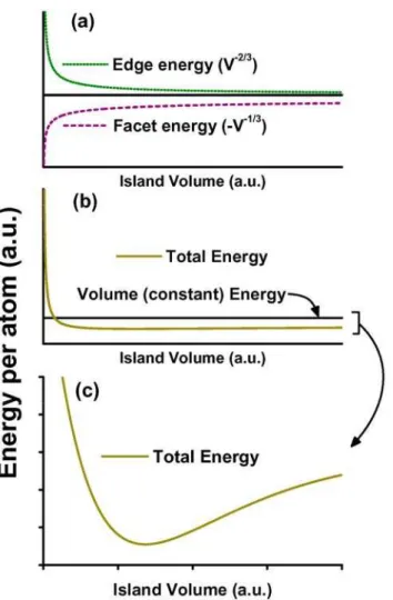
u u =α43 ⋅V−13 +
Total . (2.14)
Fig. 2.2 – Steps of Ge growth on Si(001). (a) Wetting layer formation. (b) pyramid islands nucleation for
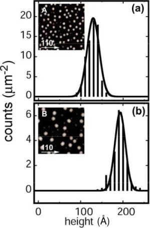
coverages Θ > ~3.5 ML. (c) Island shape transition to domes for Θ > ~6ML. Typical pyramid and dome
islands are shown with their dimensions (scanning tunneling microscopy images from [Rastelli02]).
![Fig. 2.3 – Phenomenological model for Stranski-Krastanov island shape transition [Shchukin95]](https://thumb-eu.123doks.com/thumbv2/123dok_br/15830791.137672/50.918.172.757.355.765/phenomenological-model-stranski-krastanov-island-shape-transition-shchukin.webp)
![Fig. 2.6 – Angular scans along the [1-10] direction at different local lattice parameters a’ (q r positions), for the dome sample (a) and for the pyramid sample (b)](https://thumb-eu.123doks.com/thumbv2/123dok_br/15830791.137672/55.918.130.804.116.531/angular-direction-different-lattice-parameters-positions-pyramid-sample.webp)