Growth Structural and Optical Properties of the Thermally Evaporated Tin Diselenide (SnSe2) Thin Films
Texto
Imagem

Documentos relacionados
In general, it is possible to see that the relative emission intensity of these bands is different at each point, so the PL spectra depends on laser spot position as it can be
transmittance and low electrical resistivity, the effect of the Nb-doping and the pulsed bias on the electrical and optical properties of oxygen deficient Ti 2 O 3 thin
“Structure, optical, and electrical properties of indium tin oxide thin films prepared by sputtering at room temperature and annealed in air or nitrogen.” In: Journal of applied
Single-layer films were grown using Si (100) and glass substrates and different deposition times, substrate temperature and the organometallic temperature, while the other
In this work tungsten oxide thin films were obtained by thermal evaporation on (100) silicon substrates covered with gold and heated at 350 and 600 °C, with different
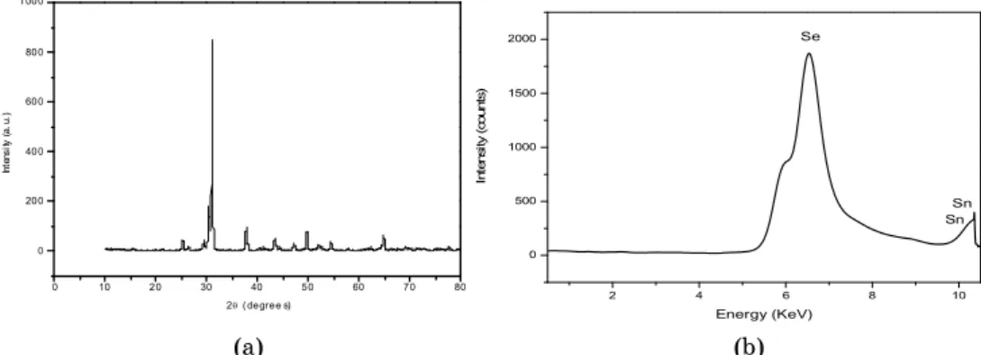
The type of electrical conduction ( p -type) in SnSe thin films was verified using the hot-probe method while Temperature depended electrical reisitivity measurement of
Figure 2(a&b) shows the transmittance and absorption spectrum of CdS thin films deposited at different molarity concentration 0.10M and 0.20M .The spectra recorded for CdS
Fig.2. Average friction coefficient of investigated films against alumina at a room and elevated temperatures, normal load applied of 1 N.. The testing at elevated temperature led to
