© Author(s) 2006. This work is licensed under a Creative Commons License.
Radio Science
Configurable multiplier modules for an adaptive computing system
O. A. Pf¨ander1, H.-J. Pfleiderer1, and S. W. Lachowicz2
1Microelectronics Department, University of Ulm, Germany
2School of Engineering and Mathematics, Edith Cowan University, Perth, Western Australia
Abstract. The importance of reconfigurable hardware is in-creasing steadily. For example, the primary approach of using adaptive systems based on programmable gate arrays and configurable routing resources has gone mainstream and high-performance programmable logic devices are rivaling traditional application-specific hardwired integrated circuits. Also, the idea of moving from the 2-D domain into a 3-D design which stacks several active layers above each other is gaining momentum in research and industry, to cope with the demand for smaller devices with a higher scale of integration. However, optimized arithmetic blocks in course-grain recon-figurable arrays as well as field-programmable architectures still play an important role. In countless digital systems and signal processing applications, the multiplication is one of the critical challenges, where in many cases a trade-off be-tween area usage and data throughput has to be made. But the a priori choice of word-length and number representation can also be replaced by a dynamic choice at run-time, in or-der to improve flexibility, area efficiency and the level of par-allelism in computation. In this contribution, we look at an adaptive computing system called 3-D-SoftChip to point out what parameters are crucial to implement flexible multiplier blocks into optimized elements for accelerated processing. The D-SoftChip architecture uses a novel approach to 3-dimensional integration based on flip-chip bonding with in-dium bumps. The modular construction, the introduction of interfaces to realize the exchange of intermediate data, and the reconfigurable sign handling approach will be explained, as well as a beneficial way to handle and distribute the nu-merous required control signals.
1 Introduction
Today’s ever-increasing demand for computing power in vir-tually all application sectors, including the emerging
pho-Correspondence to: O. A. Pf¨ander
ALU
REG PE
ICS ICS
PE
REG ALU
ICS
PE
REG ALU
ICS
PE
REG ALU
ICS
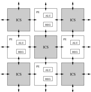
Fig. 1. The starting point is a 2-dimensional course-grain soft
re-configurable array of processing elements (PEs) and intelligent con-figurable switches (ICS).
vertical integration of two 2-D chips, are becoming an at-tractive solution to combat the rising requirements for inter-connect wires (Davis et al., 2005).
This paper is organized as follows: Sect. 2 reviews the 3-D-SoftChip adaptive computing system and its approach to architectural mapping and vertical integration, Sect. 3 con-centrates on the design of embedded multiplier blocks into the 3-D-SoftChip’s processing elements, and Sect. 4 con-cludes the paper and gives suggestions for further investiga-tion.
2 3-D-SoftChip adaptive computing system
The concept of the 3-D-SoftChip adaptive computing sys-tem is located in the intersection of three major fields of re-search: Modern very large scale integration (VLSI) in deep sub-micron IC design, reconfigurable hardware, and 3-D in-tegration. This section will at first highlight the basic method of transforming a 2-dimensional course-grain reconfigurable array into a sophisticated 3-dimensional integrated system, then mention the architectural mapping approach and also present the vertical integration method using indium bumps. 2.1 2-D to 3-D transformation
The starting point for the transformation into the 3-D-SoftChip system is a 2-dimensional course-grain soft recon-figurable array of processing elements as depicted in Fig. 1. Each processing element (PE) contains arithmetic and
log-PE PE
PE
PE PE
PE PE
PE PE PE
PE PE
PE PE
PE PE
ICS ICS
ICS
ICS
Fig. 2. Functional separation into a sea of PEs and an array of ICS
blocks. Each ICS connects a group of 4 PEs using vertical wiring resources.
ical functional blocks combined in an arithmetic logic unit (ALU) and also buffer elements (registers, REG). The ALUs are designed for increased flexibility in order to support vari-able data word-lengths for various types of computation. The overall layout is very much like a checkerboard, with intel-ligent configuration switches (ICS) accessing the surround-ing PEs through a next-neighbor interconnect scheme. Thus, each ALU is able to communicate with all adjacent ALUs through the ICS which serves as a cross point switch with embedded memory.
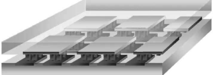
Fig. 3. To achieve a vertical 3-dimensional integration of the upper
ICS chip and the lower CAP chip, indium bumps are used for flip-chip bonding.
2.2 Vertical integration
As described in the previous subsection, the sea of PEs is now separated from the array of ICS blocks. The lower chip that now contains the PEs only is called the configurable ar-ray processor (CAP). The transformation of the planar 2-D architecture through the approach depicted in Fig. 2 into two vertically integrated chips, namely the upper ICS chip and the lower CAP chip, is illustrated in Fig. 3.
Each of the two chips has an array of aluminum pads on the top metallization layer, each with a size of 10µm×10µm. The pad pattern on the lower chip is a mirror image of the upper chip’s pattern. When the chips are placed face-to-face on top of each other, this creates an interface for a vertical connection between them, and the actual con-nection is realized by depositing indium bumps onto the alu-minum pads on the upper and lower chip, respectively. Cre-ating the bumps comprises the following processing steps: After the silicon substrate has been oxidized and the alu-minum pads have been patterned the normal way, there is an additional photoresist coating and patterning step involved to cover and protect the pads’ surrounding die surface. Then, ti-tanium (as a diffusion inhibitor), gold (as a contact layer) and indium get evaporized and thus brought onto the aluminum pads. After the lift-off, there is an extra reflow process to make use of the surface tension of the low-melting indium material, in order to transform the block-shaped deposits into bumps with an increased height-to-width ratio. This ensures a certain self-adjusting capability once the two chips get con-nected (Pf¨ander et al., 2005). The bumps have a diameter of about 7.5µm after reflow. The upper ICS chip is flipped and bonded face-down to the lower CAP chip, then the space be-tween is filled with a curing material to ensure a mechanical stability.
2.3 Architectural mapping
The upper chip’s function (ICS) is to act as a massively par-allel cross point switch as well as a parpar-allel interconnected buffer memory, to allow for a very high-speed data manipu-lation within the plane. The lower chip (CAP) is a highly par-allel array of soft-programmable processing elements, which
is capable of carrying out complex calculation tasks directly on data stored in the CAP plane or – using the 3-D terconnect – stored in the top plane. Each of the PEs in-cludes its own embedded register file, along with functional ALU blocks, glue logic and instruction decoding circuitry. Software-programmed instructions are forwarded globally to all processors from on-chip RAM. Even transforms and other processing tasks may be carried out according to embedded software instructions on the highly parallel sea-of-PE array. Two levels of hierarchy within the CAP architecture facili-tate the configuration of the ALU’s word-length: While at the first level, four processors and one ICS are utilized, this basic group can communicate with adjacent groups at the second level. The interconnection between the parallel array pro-cessors is provided by a bus architecture for rapid extraction or insertion of data. Due to the programmable nature of the CAP, the system is highly flexible, and as a result of the ver-tical interconnects and highly parallel configurable architec-ture, the efficiency is improved compared to the 2-D planar architecture that was the starting point. On the array level in the system, addressing will follow a switched bus archi-tecture. The multi-tasking requirement of the system intro-duces a particular need for formulating the architecture that is driven by a variable and configurable number of bits. There-fore, the identification of generic primitives such as adders and multipliers suitable for word-length expansion becomes an important task to realize a higher system flexibility with-out compromising performance.
3 Configurable multiplier modules
3.1 Heterogeneous processing elements in the CAP For generic ALU functions, the 3-D-SoftChip’s standard PE is optimized for bit-level computation. However, when it comes to frequently used arithmetic functions – e.g. in signal processing applications where the data path con-tains many multiplication steps involving constantly chang-ing filter coefficients – it becomes more efficient to imple-ment fixed-wired and dedicated functional blocks instead of combining the configurable logic (Haynes et al., 1999). This approach is now common practice in modern high-performance FPGA designs, like the Xilinx Virtex-II Pro that uses 18×18 bit multiplier hard IP blocks strategically placed on the chip (Xilinx, 2005). Introducing a processing acceler-ator PE with embedded special blocks (Pf¨ander et al., 2005), such as a barrel shifter or an accumulator/subtractor unit, helps to reduce the data transfer and increases the compu-tation efficiency. There is only a medium flexibility trade-off compared with a complete homogeneous type PE array.
impor-S_IN(1)A(1) S_IN(0) A(0)
B(0)
B(1)
B(2)
PSL_IN(2) PSL_IN(1)
CTRL_V CTRL_I_1 CTRL_C_1
C_OUT(0) PSL_IN(0) C_OUT(1)
C_OUT(2)
CTRL_C_2
C_IN(2) C_IN(1) C_IN(0)
CTRL_I_2
A(2)
0 0
0
CTRL_H 0 S_IN(2) 0 0
M(0) M(1) M(2) M(3) M(4) M(5)
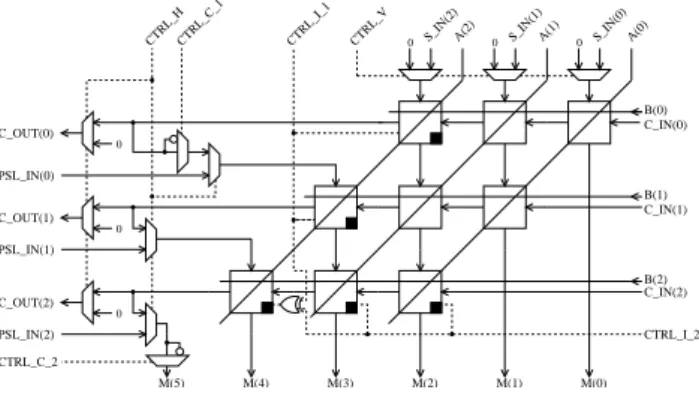
Fig. 4. A parallel-parallel modified Baugh-Wooley array multiplier
with multiplexer-based interfaces
tant and widely used mathematical operations and requires a large amount of hardware resources when implemented in a straight-forward way. Instead of that, we have come up with a modular multiplier design that enables the system to com-pute at a configurable word-length, which will be explained in the following.
3.2 Basic scheme and module characteristics
With the concept of arithmetic operations accommodating word-lengths that are configurable at run-time, a digital hard-ware circuit can adapt to changing accuracy requirements easily and fast. With little overhead, new extensions can help to improve the embedding of multiplier architectures in the surroundings of the 3-D-SoftChip system. As was presented in Pf¨ander and Pfleiderer (2004), we have designed differ-ent variants of multiplier modules that rely on a multiplexer-based connectivity extension for an intermediate data ex-change. The general idea is to tap the flow of carry and output bits in specific positions inside an array of basic cells. These cells compute the partial product and provide sum and carry, and with the help of multiplexers and corresponding control signals, the module’s behavior can be directly influenced at run-time. The flexible word-length architecture and its dy-namic reconfigurability provides either a higher throughput at low levels of precision or a higher precision by grouping multiple elements together, thus greatly increasing the de-sign’s efficiency. Also, since every module is a fully func-tional multiplier itself, a high parallelism can be achieved when all modules compute separately.
The basic modular building block is ann×nbit multiplier. By concatenatingm×mof these uniform blocks through the use of interconnect resources, in our case also involving the vertical inter-chip interface, a superior(m×n)×(m×n)bit multiplier is formed that enables the computation at flexible precision in steps ofn. The input operand word-lengths of the multiplier elements do not necessarily have to be equal, a scheme ofn1×n2bit withn16=n2is also possible.
Fig. 5. A concatenation of four 3×3 bit multiplier modules creates
a 6×6 bit superior multiplier. (Control signals not shown for better overview)
3.3 Realization options
Starting from an unchanged parallel-parallel array multiplier core (Hwang, 1979), there are different expansion steps re-quired in order to achieve the desired connectivity options. Here, since we are dealing with signed numbers, this de-mands extra sign handling circuitry. An architecture compar-ison in terms of hardware usage and complexity has shown that the modified Baugh-Wooley design (Baugh and Woo-ley, 1973) offers the least overhead of the proposed two’s complement multipliers, since there is no need for a sign extension (Pf¨ander and Pfleiderer, 2004). The modified de-sign incorporates the data exchange interfaces mentioned in the previous subsection and the possibility to handle differ-ent number represdiffer-entations, due to the modified and config-urable basic cells in specific array positions. It can handle the following number systems: Unsigned (when the special cells are configured to act without negating the partial prod-uct), Signed-Magnitude (when the sign bit is calculated ex-ternally, namely utilizing an XOR gate) and Two’s Comple-ment (Pf¨ander et al., 2005).
Figure 4 shows ann=3⇒3×3 bit parallel array multi-plier as an example, and Fig. 5 represents a concatenation of four modules to form an(m=2;n=3)⇒6×6 bit mul-tiplier. The control signals are used to control the interfaces and also the configurable partial product inversion step in the special basic cells, in order to obey the mathematical require-ments given in Baugh and Wooley (1973). The signals are mapped according to the position in the concatenation and the desired number system using a control decoder in order to save I/O and interconnect resources. Thus, a part of the ICS control logic is transferred onto the CAP plane and inte-grated into the multiplier modules.
FF FA
B(0) Cb(0)
FF FF
FA (MSB first)
Cb S_IN
A with LSB first Ca with LSB first
Ca
S_OUT Adder
FF B(3)
Cb(3)
FF FF
FA B(2)
Cb(2)
FF FF
FA B(1)
Cb(1)
Fig. 6. The modified Baugh-Wooley multiplier can also be realized
in a serial-parallel way. The first multiplicand and the control signal vector are fed in serially.
3.4 Comparison of multiplication schemes
Looking at the schemes shown in Figs. 4 and 6, it becomes evident that the number of basic cells N is a function of the word-length. For the parallel arrayN∝n2and for the serial-parallel multiplierN∝n. Note that the serial-parallel multiplier’s alleged area advantage is compensated by the expenses for the shift registers needed to store one input operand and the control vector. However, both options have in common that considerable overhead to enable the connec-tivity is entailed, for example 40% atn=4 for the parallel array (Pf¨ander and Pfleiderer, 2004). It is not sufficient to judge from the schematic hardware overhead alone; for a fair comparison, the following aspects have to be considered ad-ditionally:
– Area usage – depending on the available technology and cell library etc.
– Computation time – since the serial-parallel approach uses 2nclock periods
– Data throughput
In order to increase the data throughput, a fully pipelined parallel array is possible, but more than 5n2extra registers would be necessary, resulting in even higher area penalty and increasing the complexity of a processing element. Thus, the decision which approach to use depends on a multitude of pa-rameters. The range of applications plays the dominant role by asserting the claims for throughput and speed, and also other restrictions in terms of area usage and power consump-tion may apply. In general, the connectivity opconsump-tion requires a considerable extra amount of circuitry in each processing element.
4 Conclusion
In this paper, we have reviewed the 3-D-SoftChip adaptive computing system and highlighted the 2-D to 3-D transfor-mation and its architectural mapping. To achieve a high level of integration, a novel flip-chip bonding technique based on indium bumps on aluminum pads is used to build a system-in-a-package. The indium bumps enable a 3-dimensional
routing between the lower configurable array processor chip and the upper intelligent configurable switch chip. Look-ing at the heterogeneous processLook-ing elements located on the lower CAP chip, we have presented configurable embed-ded multiplier modules for accelerated processing. These modules are based on a modified Baugh-Wooley multiplier and expanded by multiplexer-based data exchange interfaces to provide a connectivity option. Both parallel-parallel and serial-parallel array multiplication schemes are possible, and three different number systems – namely unsigned, signed-magnitude and two’s complement – can be handled. By con-necting multiple multiplier elements together via 2-D or 3-D interconnect resources, a superior multiplier computing at an increased word-length is formed. Thus, the multiplication word-length can be chosen at run-time by dynamically real-izing a concatenation of separate modules. There is a signif-icant amount of extra hardware needed to make the dynamic array arrangement possible. But when the word-length of an optimized arithmetic unit is not fixed but can be chosen dy-namically at run-time, this opens the door for multi-precision algorithms as well as a massively parallel and efficient usage of resources in the 3-D-SoftChip system.
As an outlook on future work, the impact of a certain choice of processing element architecture on the actual area usage as a function of the specific technology parameters will become necessary. Then, more detailed conclusions about hardware overhead, area efficiency and required interconnect resources can be made. A refinement of the architecture con-cepts as well as a design space exploration in consideration of the high-potential 3-D integration approach using indium bumps are currently in the process.
References
Baugh, C. R. and Wooley, B. A.: A Two’s Complement Parallel Array Multiplication Algorithm, IEEE Trans. Computers, C-22, 1045–1047, 1973.
Bermak, A., Martinez, D., and Noullet, J.-L.: High-Density 16/8/4-bit Configurable Multiplier, IEE Proc. Circuits Devices Systems, 144, 272–276, 1997.
Davis, W. R., Wilson, J., Mick, S., Xu, J., Hua, H., Mineo, C., Sule, A. M., Steer, M., and Franzon, P. D.: Demystifying 3D ICs: The Pros and Cons of Going Vertical, IEEE Design & Test of Computers, 22, 498–509, 2005.
Eshraghian, S., Lachowicz, S., and Eshraghian, K.: Ultra High Bandwidth Image and Data Processing using 3-D Vertically Inte-grated Architectures, Proceedings of the SCI 2003, Orlando, FL, X, 189–195, 2003.
Haynes, S. D., Ferrari, A. B., and Cheung, P. Y. K.: Flexible Recon-figurable Multiplier Blocks suitable for enhancing the Architec-ture of FPGAs, Proceedings of the IEEE 1999 Custom Integrated Circuits Conference, San Diego, CA, 191–194, 1999.
Hwang, K.: Computer Arithmetic – Principles, Architecture, and Design, John Wiley and Sons, New York, 1979.
Transactions on VLSI systems, 2004.
Pf¨ander, O. A. and Pfleiderer, H.-J.: Dynamische Rekonfiguration von arithmetischen Einheiten auf Bitebene, Advances in Radio Science 2004, Miltenberg, Germany, 319–323, 2004.
Pf¨ander, O. A., Lachowicz, S. W., and Pfleiderer, H.-J.: Flexible Multiplier Blocks for Accelerated Processing in a 3D-SoftChip Adaptive Computing System, Proceedings of the IFIP VLSI-SoC 2005, Perth, Western Australia, 485–491, 2005.