JOURNAL OF NANO- AND ELECTRONIC PHYSICS Р А А - А Р
Vol. 5 No 3, 03002(3pp) (2013) Том 5 № 3, 03002(3cc) (2013)
2077-6772/2013/5(3)03002(3) 03002-1 2013 Sumy State University
Synthesis of Cerium Dioxide High-k Thin Films as a Gate Dielectric in MOS Capacitor
Anil G. Khairnar, Y.S. Mhaisagar, A.M. Mahajan*
Department of Electronics, North Maharashtra University Jalgaon, 425001, Maharashtra, India
(Received 24 December 2012; revised manuscript received 04 July 2013; published online12 July 2013)
In the present study, the Al/CeO2 / p-Si MOS capacitor was fabricated by depositing the Aluminium (Al) metal layer by thermal evaporation technique on sol-gel derived CeO2 high-k thin films on p-Si sub-strate. The deposited CeO2 films were characterized by Ellipsometer to study the refractive index that is determined to be 3.62. The FTIR analysis was carried out to obtain chemical bonding characteristics. Ca-pacitance-voltage measurements of Al/CeO2 /p-Si MOS capacitor were carried out to determine the dielec-tric constant, equivalent oxide thickness (EOT) and flat band shift (VFB) for the deposited CeO2 film of 16.22, 1.62 nm and 0.7 V respectively. The conductance voltage curve was used to determine the interface trap density (Dit) at the CeO2 / p-Si interface that is calculated to be 1.29 × 1013 cm– 2 eV– 1 for measure-ment frequency of 500 kHz.
Keywords: High-k, CeO2, Gate dielectric, Sol-gel, XRD, FTIR.
PACS numbers: 77.55. + f, 81.20.Fw, 68.37, Hk, 85.30.Tv, 84.37. + q.
1. INTRODUCTION
The scaling of devices in current ultra large scale integrated (ULSI) circuits reached to a limit where SiO2 gate dielectrics has been replaced by alternate high dielectric constant (high-k) oxides in order to over-come the gate delay and other related issues [1-3]. It is clear from the development of high-k materials that only replacing the gate insulator may not be sufficient for device scaling. Hence, the research is focused on developing the novel high-k / metal gate (HK/MG) stacks in order to enhance the performance of the de-vices. The poly depletion effects and the Vt pinning at
the high-k/polysilicon interface can be eliminated while providing higher channel mobilities by selecting a com-patible metal gate electrode with the high-k gate die-lectric material [4] by finding dual-band edge metals that are compatible with the high-k dielectric. The high-k materials used in gate stack must have high permeability, thermal stability, good quality of film and interface property, processing and material compatibil-ity with fabrication of CMOS devices and long term reliability [5]. Sol-gel technology allows the deposition of thin films of controlled thickness with the additional advantage that, it is also possible to dope them with a large variety of organic and inorganic compounds, sub-stantially increasing the range of possible applications in many fields of science and technology [6-7]. Stable chemical properties, compatibility with silicon, ease of processing, high oxygen diffusivity and high dielectric constant with low leakage current density make CeO2 remarkable as gate dielectrics for MOS devices [8, 9, 10], an electrolyte material for integrated solid oxide fuel cells (SOFC) and buffer layers between silicon and other functional ceramics, such as PbTiO3 and Pb (Zr,Ti)O3 [11]. However, it has been consistently ob-served that high-k based MOSFETs have problems such as reduced mobility of electronic carriers in the transistor channel, difficulty in setting the threshold voltage for both PMOS and NMOS devices, (Vth)
insta-bility, and other device reliability problems [12-13]. Further improvement requires a fundamental
under-standing of these phenomena. The MOS capacitor ap-plications using CeO2 thin films as a high-k oxide, de-posited by metal organic decomposition (MOD) on Si, 4H-SiC, GaN have been recently reported by other re-searchers [14, 15, 16]. In this investigation, the Al / CeO2 / p-Si MOS capacitors were fabricated by de-positing Al on sol gel deposited CeO2 thin films. The expe-rimental work carried out for CeO2 thin films dep-osition is described in second part of the paper. The results are discussed in third part and the fourth part concludes the paper.
2. METHODS AND MATERIALS
A.G. KHAIRNAR,Y.S. MHAISAGAR,A.M. MAHAJAN J. NANO- ELECTRON. PHYS. 5, 03002 (2013)
03002-2 3. EXPERIMENTAL RESULTS AND
DISCUSSION
3.1 Fourier-transform infrared spectroscopy (FTIR)
Fig. 1 –FTIR spectra of deposited CeO2 film
The FTIR analysis was carried out to obtain infor-mation about chemical bonding characteristics using the FTIR spectrometer. The Fig. 1 shows the IR spectra of the deposited CeO2 thin film. The spectrum is shown in range 500-800 cm– 1. The spectrum shows the exist-ence of Ce oxide phases. The peaks from 500-800 cm– 1 are due to presence of Ce-O bond [17]. In the present spectra of the CeO2 film, the Si-O band appears at 1050 cm– 1 (not shown in the spectra) the broad O-H bond has been detected at 3402 cm– 1 (not shown in the spectra) may be due to the presence of moisture, how-ever, it can be reduced by annealing the deposited CeO2 films at higher annealing temperatures.
3.2 Ellipsometer
The deposited films were characterized by Ellipsome-ter to study the thickness and refractive index profile of the films. The equivalent oxide thickness (EOT) of the deposited film is calculated using the relation EOT = (3.9 ×thigh-k) / khigh-k. The effect of variation in mole
ratio of citric acid on thickness of deposited CeO2 film has been observed to be noteworthy and the EOT determined for the deposited CeO2 thin films is 1.19 and 1.79 nm, for the physical thickness of 4.94 nm and 7.44 nm for 1:1.0 and 1:1.5 molar ratio respectively. The refractive index of the deposited CeO2 film has been measured using the Ellipsometer at the visible wavelength of 632.8 nm is 3.615. It was studied that solutions containing larger citric acid amount produce thicker films due to citric
ac-id’s ability to promote sol’s gelation [18]. Citric acid facil i-tates the dissolution process of cerium chloride in ethanol due to a unidentate complex formation between the ceri-um cation (Ce3 +) and the COO- group of citric acid, there-by leading to highly homogeneous and uniform films as reported by A. Verma et al. [19].
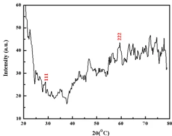
3.3 XRD
The crystal structure of the film is verified with the X-ray diffraction (XRD); Fig. 2 shows the XRD spectra of CeO2 film. CeO2 peaks with JCPDS card no. 81-0792 were detected. Two diffraction peaks, which were
as-cribed to cubic phases of CeO2, were detected at (111) and (222). These peaks are in well agreement with the CeO2 films deposited by MOD [10].
Fig. 2 – XRD spectra of deposited CeO2 film
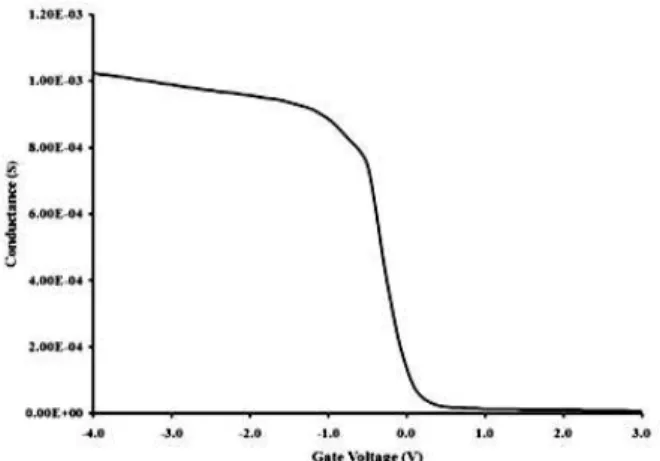
3.4 Capacitance-Voltage (C-V) characteristics
Al/CeO2/p-Si MOS capacitor was characterized by the Agilent 4284A LCR meter for the measurements of elec-trical properties of the fabricated MOS structure. A typi-cal C-V characteristics curve of MOS structure is shown in the Fig. 3. The dielectric constant determined from accumulation capacitance of CV curve, physical thick-ness of CeO2 layer and electrode area of 3.14 × 10– 4cm2 obtained at 500 kHz is 16.22. This k value is lower than the ideal (k 26) may be due to the growth of low-k in-terface layer between substrate (p-Si) and high-k (CeO2) during annealing in the open air furnace. There is a slight negative shift (0.7-0.8 V) in the flat-band voltage (VFB), which indicates the presence of positive fixed
charges near the CeO2 / Si interface. The value of inter-face trap density (Dit) is determined from the parallel
capacitance conductance model using C-V and conduct-ance- voltage (G-V) curves of Fig. 3 and 4 as previously reported by Khairnar et al. [20].
Fig. 3 – С-V characteristics of the Al/CeO2/Si MOS capacitor
SYMTHESIS OF CERIUM DIOXIDE HIGH-K THIN FILMS… J. NANO- ELECTRON. PHYS. 5, 03002 (2013)
03002-3
Fig. 4 – С-V characteristics of the Al/CeO2/Si MOS capacitor
Fig. 5 –Variation of dielectric constant with measurement frequency
1013 eV– 1 cm− 2. The obtained value of D
it can be
mini-mized further by annealing these CeO2 films at higher
annealing temperatures. The dependence of the dielec-tric constant of the deposited films on the measurement frequency is shown in figure 5. It is observed that the dielectric constant decreases with increase in the meas-urement frequency [11]. This decrease in k value due to the fact that, the dielectric constant is the function of capacitance and capacitance is the function of measure-ment frequency.
4. CONCLUSIONS
The FTIR spectra clearly show the presence of the CeO2 film, deposited by sol-gel spin coating technique in the range of 500-800 cm– 1. The XRD shows the crys-talline structure of deposited CeO2 films. The Dit value results in slight leakage in current but that can be con-trolled with annealing films at higher temperature. We have determined dielectric constant of 16.22 and EOT of 1.62 nm for the deposited CeO2 film with 1:1.5 mole ratios. Therefore, based on the aforementioned proper-ties, like higher dielectric constant, the desired struc-tural and compositional properties, the deposited CeO2 thin film with 1:1.5 mole ratio of cerium chloride hepta-hydrate citric acid can be a promising alternative high-k gate dielectric layer to replace conventional SiO2 for advanced gate stack in advanced HK/MG stack tech-nology.
ACKNOWLEDGEMENT
A. G. Khairnar is thankful to CSIR New Delhi, In-dia for providing senior research fellowship for carrying out this work (vide File No. 09/728(0029)/2012-EMR-I). The financial support from University Grants Commis-sion (UGC), New Delhi, India, vide F. No. 36-181/2008(SR) is greatly acknowledged.
REFERENCES
1. Stephen Hall, Octavian Buiu, Ivona Z. Mitrovic, Yi Lu, and William M. Davey, J. Telecommun. Inform. Technol. 2,33(2007).
2. A.M. Mahajan, A.G. Khairnar, B.J. Thibeault, J. Nano- Electron. Phys.3, 647 (2011).
3. Jinwoo Kim, Seokhoon Kim, Hyunseok Kang, Jihoon Choi, and Hyeongtag Jeon, Sungkwun Back, Kyungdong Yoo, Choelhwyi Bae, J. Appl. Phys. 98, 094504 (2005).
4. Chris Auth, Mark Buehler, Annalisa Cappellani, Chi-hing Choi, Gary Ding, Weimin Han, Subhash Joshi, Brian McIntyre, Matt Prince, Pushkar Ranade, Justin Sandford, Christopher Thomas, Intel Techn. J. 12 (2) 77 (2008). 5. Supratik Guha, Vijay Narayanan, Ann. Rev. Mater. Res.
39, 181 (2009).
6. Z.J. Wang, T. Kumagai, H. Kokawa, M. Ichiki, R. Maeda, J. Electroceram. 21, 499 (2008).
7. J. Tardy, M. Erouel, A.L. Deman, A. agnaire, V. Teodorescu, M.G. Blanchin, B. Canut, A. Barau, M. Zaharescu, Microelectron. Reliab. 47, 372 (2007). 8. Gregory K.L. Goh, Christine S.S. Tay Kelvin Y.S. Chan,
N. Gosvami, J. Electroceram. 16, 575 (2006).
9. Miyuki Kouda, Kiichi Tachi, Kuniyuki Kakushima, Parhat Ahmet, Kazuo Tsutsui, Nabuyuki Sugii, Arun Chan-dorkar, Takeo Hattori, H. Iwai, ECS. Trans. 16, 153 (2008).
10.Hock Jin Quah, Kuan Yew Cheong, Zainuriah Hassan, and Zainovia Lockman, IEEE T. Electron Dev. 58, 122 (2011).
11.Jyrki Lappalainen, Harry L. Tuller, Vilho Lantto, J. Elec-troceram. 13, 129 (2004).
12.E.P. Gusev, V. Narayanan, M.M. Frank, IBM J. Res. Dev. 50, 387 (2006).
13.M. Houssa, L. Pantisano, L.-A. Ragnarsson, R. Degraeve, T. Schram, G. Pourtois, S. De Gendt, G. Groeseneken, M.M. Heyns, Mat. Sci. Eng. R51, 37 (2006).
14.H.J. Quah, K.Y. Cheong, Z. Hassan, Z. Lockman, F.A. Jasni, W.F. Lim, J. Electrochem. Soc. 157, H6 (2010). 15.W.F. Lim, K.Y. Cheong, and Z. Lockman, Appl. Phys. A
103, 1067 (2011).
16.H.J. Quah, W.F. Lim, K.Y. Cheong, Z. Hassan, and Z. Lockman, J. Cryst. Growth 326, 2 (2011).
17.Aniruddha Panda, PhD thesis “Preparation and character-ization of mesoporous CeO2-ZrO2 nanopowders using do-decylamine and sodium dodecyl sulfate as surfactant”, De-partment of Chemistry National Institute of Technology Rourkela, Orissa.
18.W. Weng, G. Han, P. Du & G. Shen, Mater. Chem. Phys. 74, 92 (2002).
19.A. Verma, A.K. Bakhshi & S.A. Agnihotry, Sol. Energ. Mater. Sol. C90, 1640 (2006).