Brazilian Microwave and Optoelectronics Society-SBMO received 21 Oct 2012; for review 7 Dec 2012; accepted 6July 2013 Brazilian Society of Electromagnetism-SBMag © 2013 SBMO/SBMag ISSN 2179-1074
Abstract— This work describes the design and optimization of a printed circuit board containing a rectangular half-loop coil designed to apply radio frequency signals on micrometric diamond crystals. The structure was optimized to maximize the magnetic field perpendicular to the coil at 2,87 GHz. In the optimization process we have used transmission line theory, circuit level and 3D electromagnetic simulations. The structure was implemented and measured. The adopted methodology was validated by the good agreement between theory and experiments.
Index Terms— Application of radio frequency magnetic fields, waveguide
optimization, printed circuit board design.
I.INTRODUCTION
Diamond crystals, either natural or artificial, may contain lattice defects capable of changing its
physical properties. One of these defects is the N-V center, a point defect consisting of a nitrogen
atom and a lattice vacancy [1]. This defect is common in diamond lattice and has potential
applications in magnetometry, quantum computation, cryptography, among other areas [1] [2] [3].
One of the main advantages of the N-V center is the atomic size of the defect. This may allow the
production of nanometric probes capable of nanometric resolution measurements. Such a probe could
be useful in spintronic devices [4] or magnetometry of living cells and microorganisms since the
properties of the N-V center can be observed even at room temperature [2] [5].
The N-V center fluorescence is the main phenomenon of the defect that can be useful for
magnetometry. The fluorescence intensity changes according to the magnetic field applied to the N-V
center. Practically speaking, a green laser (532 nm, near the absorption peak of the N-V center [6])
provides optical excitation for the N-V center. A photoemission between 600 and 800 nm occur due to
the excitation [6]. In the absence of magnetostatic fields, this emission is reduced by approximately
10% when the center is exposed to a radio frequency (RF) field at 2.87 GHz [7]. When there are both
a radio frequency field and a magnetostatic field, the emission reduction is observed in two distinct
frequencies equally spaced from the central frequency of 2.87 GHz. This frequency spacing is
proportional to the magnetostatic field intensity in the N-V center region, with a constant of
approximately 71 kHz / (A/m) [2] [7]. This method has been widely studied and it has attracted great
interest for developing magnetic field probes. These probes are suitable for nanoscaled magnetometry
and magnetic imaging systems due to the N-V center dimensions and to the high accuracy frequency
Geometry optimization for application of
radio frequency signals on diamond samples
Ricardo R. Wolf Cruz, Marlio J. C. Bonfim, Wilson A. Artuzi Junior Universidade Federal do Paraná
Curitiba, Brasil
Brazilian Microwave and Optoelectronics Society-SBMO received 21 Oct 2012; for review 7 Dec 2012; accepted 6July 2013 Brazilian Society of Electromagnetism-SBMag © 2013 SBMO/SBMag ISSN 2179-1074
measuring techniques currently available [2] [7] [8].
The RF signals are typically applied by positioning the diamond samples near transmission lines.
Common geometries for these transmission lines are micrometric sized copper wires [5] or short
circuited coplanar waveguides [9].
This work describes the optimization of a structure designed to apply radio frequency signals on
diamond samples, aiming to maximize the magnetic field at the desired frequency. This work focuses
on diamond samples, however it is suitable for application of RF magnetic fields to any desired
material, limited only by it's physical dimensions. The design considered commonly available
materials and production processes, using a printed circuit board (PCB) as the main structure,
providing good repeatability. Calculations and simulations where performed to maximize the RF
magnetic field perpendicular to the plane of the board [5] at the frequency of 2.87 GHz in order to
reduce the power constraints of the RF generator.
II. BASE GEOMETRY A. Limitations and design rules
The manufacturing process, from a PCB industry [10], has some dimensional restrictions. Both the
minimum spacing between tracks and the minimum track width are equal to 155 m and the external
board dimensions must be 70 mm x 20 mm. This keeps the dimensions of the board mechanically
compatible with the prototype developed for the N-V center study (a home-built optical microscope,
containing auxiliary systems to provide optical excitation, photodetectors, etc). The samples should be
placed near the center of the board, so the structure designed to apply the RF on the samples can be
placed in that region. For compatibility reasons the RF input port is provided by 23 mm long SMA
connector.
B. Chosen Geometry
The chosen structure to apply RF magnetic fields has the shape of a half-loop coil. This maximizes
the magnetic field on the samples and keeps the flat geometry required by the manufacturing process.
In order to simplify the drawing process, the half-loop is made only of straight sections. The final
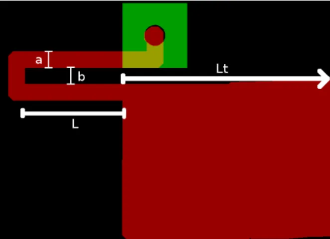
appearance of the half-loop is analog to the U letter, as shown in Fig. 1.
The copper region on the right side of Fig. 1 represents a section of a 50 Ω microstrip line with
length Lt. The optimization of this waveguide will be explained further. It connects the half-loop to
the SMA connector where the RF signal is applied to the board. The other end of the half-loop is
connected to the ground plane (GND) through a via hole. The diamond sample should be placed in the
Brazilian Microwave and Optoelectronics Society-SBMO received 21 Oct 2012; for review 7 Dec 2012; accepted 6July 2013 Brazilian Society of Electromagnetism-SBMag © 2013 SBMO/SBMag ISSN 2179-1074
Fig. 1. Half-loop design for the RF application. Red regions are made of cooper, the green region represents a pad containing a via connecting the half-loop to the ground plane on the back. The dimensions a and b are equal to 155 m each, representing the half-loop width and the inner spacing of the loop respectively. L is the half-loop length, and Lt the length of
the waveguide connecting the half-loop to the SMA connector. III. MODELING AND OPTIMIZATIONS A. Half-loop dimensioning
In order to maximize the RF magnetic field in the half-loop, the dimensions a and b where made the
smallest as possible (155 m). The length L of the half-loop must be large enough to allow easy
sample positioning, but not too large to avoid increasing the loop impedance. The maximum length
was determined from a simulation on QUCS software [11]. This simulation allowed the choice of the
maximum length that keeps the half-loop impedance below 50 Ω at the desired frequency. The
dielectric and PCB parameters used in the simulations are shown in Table I, in the “εicrostrip δine”
column. These parameters were taken from the PCB manufacturer.
The half-loop was modeled as transmission line sections. The sections with length L (Edges 1 and 3
in Fig. 2) where modeled using the “Coupled εicrostrip δine” distributed element, which considers
the auto-coupling effect due to the proximity of the parallel sections. The section “Edge 2” was
modeled with the element “εicrostrip δine”. To complete the structure of the half-loop, elements
“εicrostrip Corner” and “εicrostrip Via” were used, as shown in Fig. 2.
Fig. 2. Schematic of the half-loop model used in the QUCS simulations. Edge 1 and 3 are “Coupled εicrostrip δine”
element, Edge 2 is a “εicrostrip δine” element. The corners are “εicrostrip Corner” elements.
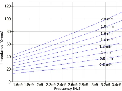
A parameter sweep was performed for the length L, ranging from 0.6 mm to 2 mm. In the
Brazilian Microwave and Optoelectronics Society-SBMO received 21 Oct 2012; for review 7 Dec 2012; accepted 6July 2013 Brazilian Society of Electromagnetism-SBMag © 2013 SBMO/SBMag ISSN 2179-1074
half-loop length was chosen to be 1 mm to keep the impedance of the structure below 50 Ω up to
3,4 GHz, as shown in Fig. 3.
Fig. 3. Impedance magnitude simulation results for various half-loop lengths L. B. Transmission line dimensioning
From the Biot-Savart law [12] it is known that the magnetic field at a point inside the coil is
proportional to the current flowing through the coil. Thus the transmission line connecting the RF
generator to the half-loop had its length Lt optimized to maximize the current flow (and thereby the
magnetic field) at 2.87 GHz.
In order to maximize the current flow, the input impedance of the board is minimized at this
frequency, thus maximizing the current injected by the RF generator. The impedance of the board is
not matched to the cable impedance (50 Ω), so the RF generator must be able to work under
unmatched condition. Signal reflections will occur due to the inductive behavior of the half-coil,
generating a stationary wave.
As an initial approach, the structure will be considered as a waveguide connected to a pure
inductive load. This approach is valid due to the highly inductive impedance of the half-loop obtained
in the simulation described above (0.522 + j41.8 at 2.87 GHz). Thus, from the transmission line
theory
Z= Z0ZL+ iZ0tan
(
β. d)
Z0+ iZLtan(
β. d)
,
(1)
where Z is the impedance seen from a desired point on the transmission line, ZL is the load impedance,
Z0 is the characteristic impedance of the transmission line, d is the distance between the desired point
and the load. β is equal to 2π/ , where λ is the wavelength at the operating frequency. In this initial
Brazilian Microwave and Optoelectronics Society-SBMO received 21 Oct 2012; for review 7 Dec 2012; accepted 6July 2013 Brazilian Society of Electromagnetism-SBMag © 2013 SBMO/SBMag ISSN 2179-1074
d=
arctan
(
−ZL iZ0)
β
.
(2)
Taking into account only the imaginary part of ZL and using tangent properties, the required length
d to make ZL equal to 0 is 0.8λ . Considering the length of the SMA connectors (23 mm,
approximately 0.32 in the connector medium), the chosen transmission line length Lt is 33 mm
(~0.57 on the transmission line at 2.87 GHz). The half-coil position was chosen near the center of the
board with the aid of the transmission line impedance transformer [12].
In order to validate the approach described above, another computer simulation was done using the
QUCS software to verify the response of both the transmission line and the half-loop together. The
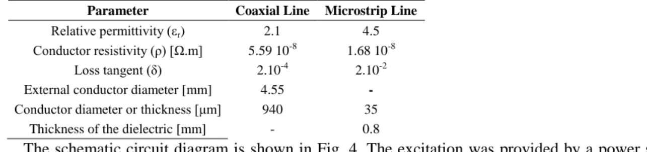
SMA connectors where modeled as “Coaxial δine” elements, using the parameters shown in Table I.
The transmission line was modeled as a “εicrostrip δine” element with characteristic impedance of
50 Ω (width of 1.47 mm). The parameters of the transmission line are shown in Table I.
TABLE I. PRINTED CIRCUIT BOARD AND SMA CONNECTOR PARAMETERS
Parameter Coaxial Line Microstrip Line
Relative permittivity (r) 2.1 4.5
Conductor resistivity (ρ) [Ω.m] 5.59 10-8 1.68 10-8
δoss tangent ( ) 2.10-4 2.10-2
External conductor diameter [mm] 4.55 -
Conductor diameter or thickness [ m] 940 35
Thickness of the dielectric [mm] - 0.8
The schematic circuit diagram is shown in Fig. 4. The excitation was provided by a power source
with output impedance of 50 Ω and power output of 0 dBm. This power output was used throughout
the optimizations though it not necessarily the power used to apply the RF signals to the samples.
Fig. 4. Circuit simulated to optimize the transmission line and analyze it's effects. The coaxial section represents the SMA connectors and the microstrip section represents the microstrip transmission line. The Half-loop block simulates the
half-loop connected to the transmission line (circuit already presented in Fig. 2).
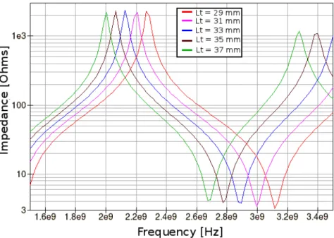
A parameter sweep of the length of the microstrip line was done to analyze the impedance as a
function of the frequency. The length Lt was swept from 29 to 37 mm. The results, shown in Fig. 5,
are consistent with the initial calculations, indicating that the length of 33 mm minimizes the
Brazilian Microwave and Optoelectronics Society-SBMO received 21 Oct 2012; for review 7 Dec 2012; accepted 6July 2013 Brazilian Society of Electromagnetism-SBMag © 2013 SBMO/SBMag ISSN 2179-1074
Fig. 5. Input impedance magnitude as a function of frequency and microstrip line length. Different lengths are represented by different trace colors.
The current waveform in the half-loop for Lt = 33 mm is shown in Fig. 6. This indicates a
maximum near 2.87 GHz, as desired.
Fig. 6. Magnitude of simulated current in the half-loop. IV. MEASUREMENTS AND COMPARISONS
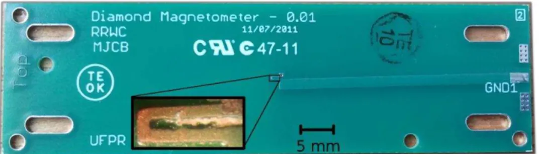
The structure implemented as a PCB is shown in Fig. 7. In order to confirm the simulation results,
Brazilian Microwave and Optoelectronics Society-SBMO received 21 Oct 2012; for review 7 Dec 2012; accepted 6July 2013 Brazilian Society of Electromagnetism-SBMag © 2013 SBMO/SBMag ISSN 2179-1074
Fig. 7. Manufactured board. The SMA connectors aren't shown in the picture. The detail shows a zoom on the half-loop. The vector network analyzer exports the data points in a Touchstone file (S2P) [13], which contains
the S parameters of the board as a function of frequency. The impedance of the board was calculated
from this file and is shown in Fig. 8. The measurement results are very close to the simulation curves
(reshown in the figure for comparison). This indicates that the modeling and the chosen parameters
are adequate, resulting in a successful project.
Fig. 8. Simulation results (lines) compared to measurements in the actual board (circles). Both phase and magnitude are shown in the figure.
The measured resonance frequencies are in good agreement with the simulation. The small
difference (~1%) at the frequency of minimum impedance is probably due to a small mismatch
between the real length of the structure and the simulated one. The impedance peaks also differs a bit,
which is probably due to dielectric losses higher than the values considered in the simulation. The
phase changes from +90° to -90° indicate the presence of resonance frequencies in the structure (at the
frequencies where the maxima and minima occur).
From the S parameters, the current was calculated under the same conditions of the simulation.
Brazilian Microwave and Optoelectronics Society-SBMO received 21 Oct 2012; for review 7 Dec 2012; accepted 6July 2013 Brazilian Society of Electromagnetism-SBMag © 2013 SBMO/SBMag ISSN 2179-1074
Fig. 9. Magnitude of simulated and measured current. V. MAGNETIC FIELD ESTIMATION
The magnetic field in the sample region can be estimated from the simulated current in the
half-loop. For this purpose we have used the software COMSOL [14], which can perform electromagnetic
simulations using the finite element method.
Due to the computational costs of the simulation and to reduce the simulation time, only a section
of the board containing the half-loop and a fraction of the 50 Ω waveguide were considered. The
simulated fraction of the FR4 dielectric material has 6 mm x 4 mm which is immersed in a fraction of
an air sphere with diameter equal to 11 mm. The dielectric and cooper thicknesses are the same of the
“εicrostrip δine” presented in Table I. The entire structure is shown in Fig. 10.
Perfect magnetic conductor boundary condition was applied to the boundaries on the same face of
the RF input, simulating a long 50 Ω waveguide, since only a small sector of the waveguide is
included in this simulation (~ 2 mm). On the other faces, scattering boundary condition was applied to
minimize signal reflections on the boundaries of the computational space. A lumped current port was
used to provide the excitation to the structure. The excitation waveform was obtained from a QUCS
simulation. This waveform was extracted at the same position of the lumped port in the COMSOL
Brazilian Microwave and Optoelectronics Society-SBMO received 21 Oct 2012; for review 7 Dec 2012; accepted 6July 2013 Brazilian Society of Electromagnetism-SBMag © 2013 SBMO/SBMag ISSN 2179-1074
Fig. 10. Structure simulated in the COMSOL software. The blue region represents copper. The fraction of sphere surrounding the structure have the air material applied to it. The dimensions of the FR4 parallelepiped representing the board
are 4 mm x 6 mm.
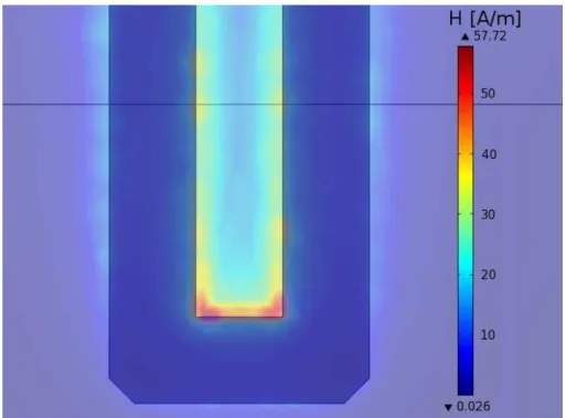
According to the simulation, the maximum current flowing into the board for a RF power input of
0 dBm is 11.8 mA. For this condition, the value of the magnetic field perpendicular to the plane of the
board and in the center of the half-loop is 22 A/m. The magnetic field is quite uniform in the center
region of the half-loop, as it can be seen in Fig. 11. This allows the use of large diamond samples or
multiple samples positioned together along the half-loop.
Fig. 11. Distribution of the magnitude of the magnetic field perpendicular to the plane of the half-loop.
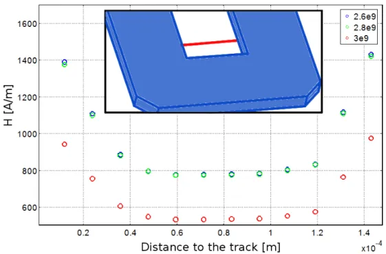
Some simulations where also performed for other RF input powers, up to 30 dBm. The estimated
Brazilian Microwave and Optoelectronics Society-SBMO received 21 Oct 2012; for review 7 Dec 2012; accepted 6July 2013 Brazilian Society of Electromagnetism-SBMag © 2013 SBMO/SBMag ISSN 2179-1074
724 A/m. A profile of the magnetic field between the tracks of the half-loop for this condition can be
seen in Fig. 12.
Fig. 12. Profile of the magnetic field between the tracks of the half-loop. The inset shows (in red) the line where the profile was calculated. Distinct frequencies where plotted in different colors. The x axis corresponds to the distance from the left
track of the half-loop. VI. TESTS WITH SAMPLES
In order to verify the half-loop efficiency to excite defects in diamond crystals, some tests applying
RF were performed. Various defects (not only N-V centers) are present in the available crystals.
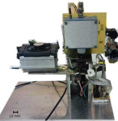
The designed board was used in an optical system built to study the fluorescence of diamond
crystals. This system includes an excitation subsystem, using a laser diode at a wavelength of 532 nm.
The system also has a home-made confocal microscope. This microscopes focuses the excitation laser
at a point in the samples. It can move the focal point in the plane of the sample with a resolution of
~150 nm. It also serves to provide a parallel beam of fluorescence to the detector. The detector uses an
avalanche photodiode combined with an transconductance amplifier to detect the fluorescence signal.
Optical filters separate the excitation and the fluorescence optical beams. A RF amplifier (30 dB gain,
40 dBm maximum output power) was also included to allow RF magnetic field intensity up to ~700
Brazilian Microwave and Optoelectronics Society-SBMO received 21 Oct 2012; for review 7 Dec 2012; accepted 6July 2013 Brazilian Society of Electromagnetism-SBMag © 2013 SBMO/SBMag ISSN 2179-1074
Fig. 13. System developed to study the fluorescence of diamond samples.
Fig. 14 shows that the influence of the RF signal in the fluorescence varies with the RF field
magnitude. The most significant reduction, of approximately 14%, was observed with an RF input
power of 40 dBm at 2.64 GHz. This results indicates that the board is suitable for applying RF signals
on small diamond samples.
Fig. 14. Influence of the RF signal in the fluorescence of a diamond sample. The RF signals were applied using the designed board. The distinct RF input powers are shown in different colors.
VII. CONCLUSIONS
The method of adjusting the transmission line length was shown suitable for maximizing the
Brazilian Microwave and Optoelectronics Society-SBMO received 21 Oct 2012; for review 7 Dec 2012; accepted 6July 2013 Brazilian Society of Electromagnetism-SBMag © 2013 SBMO/SBMag ISSN 2179-1074
were maximized in the developed structure at frequencies near 2.87 GHz.
For the circuit level simulations (using QUCS), the use of transmission line elements has proved to
be suitable for modeling the entire structure, including the half-loop. The measurements have shown
good agreement with the results obtained from the simulations for both impedance and electric
current. The simulated resonance frequencies are also similar to the measured ones.
According to COMSOL simulations, the estimated magnetic field in the sample region for a RF
input power of 30 dBm is 724 A/m. All the estimates indicate a good uniformity of the magnetic field
inside the half-loop which makes it easier to perform measurements on larger samples or with
multiple samples at once.
Initial tests with diamond crystals indicate significant influence of the RF signals in the emitted
fluorescence. The prototype could be used in future works, providing RF excitation to diamond or
others samples, allowing the investigation of the influence of magnetostatic and RF fields to the
fluorescence signal.
ACKNOWLEDGMENT
We acknowledge CAPES for the scholarship of R. R. W. C. We also acknowledge LACTEC for
providing the vector network analyzer to characterize the prototype.
REFERENCES
[1] W. L. Yang, Y. Hu, Z. Q. Yin, Z. J. Deng & M. Feng, "Entanglement of nitrogen-vacancy-center ensembles using transmission line resonators and a superconducting phase qubit", Phys. Rev. A, 83, 022302, 2011.
[2] Gopalakrishnan Balasubramanian, I. Y. Chan, Roman Kolesov, Mohannad Al-Hmoud, Julia Tisler, Chang Shin, Changdong Kim, Aleksander Wojcik, Philip R. Hemmer, Anke Krueger, Tobias Hanke, Alfred Leitenstorfer, Rudolf Bratschitsch, Fedor Jelezko & Jörg Wrachtrup, "Nanoscale imaging magnetometry with diamond spins under ambient conditions", Nature, 455, 648, 2008.
[3] Igor Aharonovich, Stefania Castelletto, David A. Simpson, Alastair Stacey, Jeff McCallum, Andrew D. Greentree, & Steven Prawer, "Two-Level Ultrabright Single Photon Emission from Diamond Nanocrystals", Nano Lett., 9, 3191-3195, 2009.
[4] C. L. Degen, "Scanning magnetic field microscope with a diamond single-spin sensor", Appl. Phys. Lett., 92, 243111, 2008.
[5] J. R. Maze, P. L. Stanwix, J. S. Hodges, S. Hong, J. M. Taylor, P. Cappellaro, L. Jiang, M. V. Gurudev Dutt, E. Togan, A. S. Zibrov, A. Yacoby, R. L. Walsworth & M. D. Lukin, "Nanoscale magnetic sensing with an individual electronic spin in diamond", Nature, 455, 644, 2008.
[6] N. B. Manson, J. P. Harrison & M. J. Sellars, "Nitrogen-vacancy center in diamond: Model of the electronic structure and associated dynamics", Phys. Rev. B, 74, 104303, 2006.
[7] Ngoc Diep Lai, Dingwei Zheng, Fedor Jelezko, François Treussart & Jean-François Roch, "Influence of a static magnetic field on the photoluminescence of an ensemble of nitrogen-vacancy color centers in a diamond single-crystal", Appl. Phys. Lett., 95, 133101, 2009.
[8] Rolf Simon Schoenfeld & Wolfgang Harneit, "Realtime Magnetic Field Sensing and Imaging using a Single Spin in Diamond", Phys. Rev. Lett., 106, 030802, 2011.
[9] G. D. Fuchs, V. V. Dobrovitski, D. M. Toyli, F. J. Heremans, D. D. Awschalom, "Gigahertz Dynamics of a Strongly Driven Single Quantum Spin", Science, 356, 1520, 2009.
[10] Circuibras, CIRCUIBRAS > PLACAS DE CIRCUITOS IMPRESSOS - Alta Tecnologia e Flexibilidade para Produção e Fornecimento de Placas de Circuitos Impressos Complexos, (2007), http://www.circuibras.com.br/, Acesso em 10/04/2012.
[11] Qucs team, Qucs project: Quite Universal Circuit Simulator, 2011, http://qucs.sourceforge.net/, Acesso em 02/04/2012. [12] Mathew N. O. Sadiku, Elementos de Eletromagnetismo, 3ª Edição, Bookman, 2004.