w w w . a j e r . o r g
Page 160
Vinay Kumar Sharma
1, Mithilesh Kumar
21, 2,
(Electronics Engg. Department, University College of Engineering, Rajasthan Technical University, India)
ABSTRACT : In this letter, a design of Compact Ultra-Wideband (UWB) bandpass filter with a switchable notch band for WLAN (5.3-5.9GHz) interference rejection is proposed. As 5.3-5.9GHz wireless local area network (WLAN) is existed in UWB spectrum range (3.1 -10.6GHz) and may interfere with UWB system operation. The UWB bandpass filter is implemented using a basic multiple mode resonator (MMR) structure feed by interdigital coupled lines for achieving higher degree of coupling. The notch band is obtained using a etched slot on main microstrip line. The centre frequency and bandwidth of notch band is optimized. The filter is compact in size with dimension 37.4 X 25 mm2.The electromagnetic simulation software, Computer Simulation Technology Microwave Studio (CST MWS) is used for the simulation and analysis of the designed structure. For fabrication of this structure Rogers RT5880 substrate of thickness 0.4 mm and dielectric constant 2.2 is used. Measured and simulated results show good agreement.
Keywords
-
WLAN, Microstrip, MMR, UWBI.
INTRODUCTION
The tremendous progress in Ultra wideband (3.1–10.6 GHz) radio technology is reported now days. The researchers’ interest rose dramatically in developing UWB devices due to its potential application in modern short distance defense and commercial communication systems. Ultra wideband (UWB) band pass filter (BPF) is an important part of and UWB communication system[1-2]. There are various types of UWB bandpass filters are reported In recent years[3-13]. To achieve low cost and easy integration, these filters are usually implemented in a microstrip or coplanar waveguide technology.
The 5.2-5.8 GHz wireless local area network (WLAN) signal is interfered with UWB system operations in the UWB in-door specification (3.1 - 10.6 GHz) standardized by U.S. (FCC). There are many designs are reported for rejecting these WLAN signals. Most of these designs used stepped impedance resonators [14], defective ground structure (DGS) [15]. The DGS structure has a serious drawback of packaging, because there is an absence of ground plane and EM field is leaked so we cannot use it for commercial fabrication purpose. Whereas stepped impedance resonators create structure too bulky and required additional space.
w w w . a j e r . o r g
Page 161
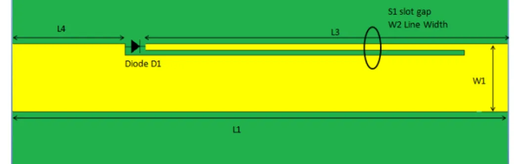
Fig. 1 Layout of the proposed UWB bandpass filter with notch bandTABLE I. Dimension of proposed filter
II.
FILTER
DESIGN
The basic UWB band pass filter is designed using a MMR structure based on stepped impedance resonator discussed in chapter three. At the central frequency of the UWB passband, i.e., 6.85 GHz, the MMR
structure composed of one half wavelength λ/2 low-impedance line section in the center and two identical λ/4 high-impedance line sections at the two sides. The low impedance section is 59.42 Ω and high impedance
section of the MMR is 138 Ω resulting in an impedance ratio of 2.32. Impedance ratio greater than 1 is utilised to design UWB filters. In this design we use Interdigital coupled lines as a I/O feed lines. The width of feed lines W is 0.3 mm and spacing S which is optimized at 0.15 mm for proper response. When giving energy to the MMR coupling energy of interdigital coupling is high compared with the single line parallel coupling.
Many designs are reported based on defective ground structure for creating notch band in a UWB passband. But due to the various drawbacks of DGS structure including the commercial packaging and fabrication problem, here we proposed a etched slot in the main microstripline in MMR structure to create a notch band. It does not require any additional structure as reduced the overall dimension.
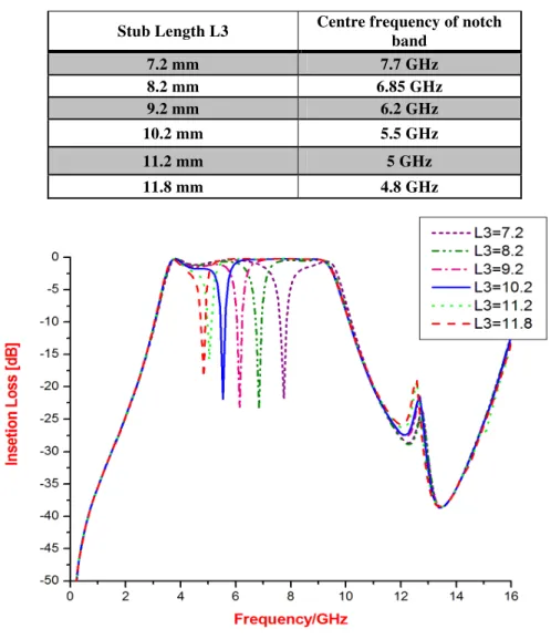
Fig. 2 shows the etched slot structure in the main microstrip line. The stub length L3 and slot gap S1 and line width W2 is optimized at 12.2 mm, 0.15 mm and 0.2 mm respectively for notch band of center frequency 5.6 GHz and bandwidth 5.3-5.8 GHz (0.5GHz). The center frequency and bandwidth of notch band varies with the parameters L3, S1 and W2.
Fig. 2 Etched slot structure for notch band realization Filter
parameter Value
Filter
parameter Value
L1 16.6mm S1 0.15mm
L2 8.25mm W 0.3mm
L3 12.2mm W1 2.1mm
L4 3.8mm W2 0.2mm
w w w . a j e r . o r g
Page 162
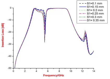
Fig. 3 Variation of centre frequency with stub length L3The bandwidth of notch band varies with the slot gap S1. The variation of bandwidth of notch band with slot gap S1 is presented in TABLE III and shown in Fig. 4 keeping L3 and W2 constant.
TABLE III. Variation of bandwidth of notch band with slot gap S1
11.2 mm 5 GHz
11.8 mm 4.8 GHz
Line Width W2 Bandwidth of notch band
0.1 mm 0.3 GHz (5.4-5.73 GHz)
0.15 mm 0.5 GHz (5.3-5.8 GHz)
0.2 mm 0.7 GHz (5.1-5.8 GHz)
0.25 mm 0.8 GHz (5.0-5.8 GHz)
0.3 mm 1.0 GHz (4.8-5.8 GHz)
w w w . a j e r . o r g
Page 163
Fig. 4 Variation of bandwidth of notch band with slot gap S1The bandwidth of notch band also varies with the line width W2. The variation of bandwidth of notch band with line width S1 is presented in TABLE IV and shown in Fig. 4 keeping S1 and L3 constant.
TABLE IV. Variation of bandwidth of notch band with line width W2
Fig. 5 Variation of bandwidth of notch band with line width W2
Line Width W2 Bandwidth of notch band
0.1 mm 0.4 GHz (5.3-5.7 GHz)
0.15 mm 0.5 GHz (5.25-5.75 GHz)
0.2 mm 0.7 GHz (5.1-5.8 GHz)
0.25 mm 0.8 GHz (5.05-5.85 GHz)
0.3 mm 1 GHz (4.9-5.9 GHz)
w w w . a j e r . o r g
Page 164
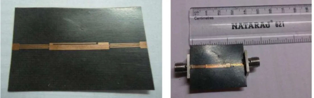
Switchable notch band characteristics is achieved using Diode D1.The substrate used is Rogers RT5880 with a relative dielectric constant of 2.2 and a thickness of 0.4 mm. Fig. 6 shows the photograph of the fabricated UWB BPF.
Fig. 6 Photograph of the fabricated UWB filter with WLAN notch
There are only simulated result of switching is presented here because switch based on lumped element could not be implemented easily in this design. When the Diode D1 is in forward bias (ON) state the EM simulated frequency response of proposed filter is shown in Fig. 7(a). The filter has the passband from 3.3 to 10.6 GHz. The passband is almost flat with attenuation around 0.3 dB in the whole passband. The return loss S11 is almost less than -10 dB in the whole passband. Group delay of proposed filter when diode D1 is ON is around 0.2 ns and overall linear in the whole pass band.
w w w . a j e r . o r g
Page 165
(b)Fig. 7 Simulated result of proposed UWB BPF when diode D1 is ON state (a) Frequency response (b) group delay result
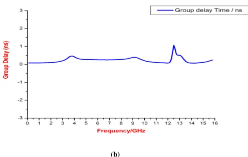
Fig. 8 (a) shows the EM simulated frequency response of proposed filter when Diode D1 is in reverse bias (OFF) state. In the OFF state we get the high selective notch band to suppress the undesired WLAN signal interference starts from 5.3 GHz to 5.8 GHz with attenuation around 25 dB. Group delay of proposed filter with notch band is around 0.2 ns and overall linear in the whole pass band as shown in Fig. 8 (b).
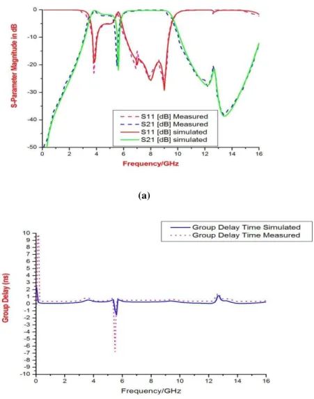
The fabricated measured results of the proposed UWB BPF with WLAN notch is presented in Fig. 5.9. The comparison of simulated and measured result is presented in Fig. 5.10, good agreement between simulated and measured results is observed. There are slight discrepancy may be due to the unexpected tolerance of fabrication and implement. In addition, the group delay within the UWB passband is between 0.56–0.85 ns, showing a good linearity.
w w w . a j e r . o r g
Page 166
Fig. 8 Simulated result of proposed UWB BPF when diode D1 is OFF state (a) Frequency response (b) groupdelay result
(a)
(b)
w w w . a j e r . o r g
Page 167
(a)Fig. 10 Comparision of simulated and fabricated measured result of proposed UWB BPF with WLAN notch (a) Frequency response (b) group delay result
IV. CONCLUSION
In this letter, a design of UWB bandpass filter with notch band for WLAN interference rejection is proposed. Here we implement a notch band in the same structure by etching out the slot in the main structure, which reduce the size because no extra circuitry is required for band stop filter. There is also switchable feature introduced using a diode. So due to its compact size 37.4 X 25 mm2and satisfactory passband and stopband performance, the filter can be useful for commercial UWB wireless communication systems.
REFERENCES
[1] S. Sun and L. Zhu, “Multimode resonator based band pass filters,” IEEE Microw. Mag., vol. 10, no. 2, pp. 88–98, Apr. 2009.
[2] Z.-C. Hao and J.-S. Hong, “Ultrawideband filter technologies,” IEEEMicrow. Mag., vol. 11, no. 4, pp. 56–68, Jun. 2010.
[3] L. Zhu, S. Sun, andW. Menzel, “Ultra-wideband (UWB) bandpass filters using multiple-mode resonator,”
IEEE Microw. Wireless Compon.Lett., vol. 15, no. 11, pp. 796–798, Nov. 2005.
[4] H.Wang, L. Zhu, andW.Menzel, “Ultra-wideband bandpass filter with hybrid microstrip/CPW structure,”
IEEE Microw. Wireless Compon.Lett., vol. 15, no. 12, pp. 844–846, Dec. 2005.
[5] B. Yao,Y. Zho, Q.Cao, andY. Chen, “Compact UWB band pass filter with improved upper-stopband
performance,” IEEE Microw. WirelessCompon. Lett., vol. 19, no. 1, pp. 27–29, Jan. 2009.
[6] S. W. Wong and L. Zhu, “Quadruple-mode UWB bandpass filter with improved out-of-band rejection,”
w w w . a j e r . o r g
Page 168
IEEE Microw.Wireless Compon. Lett., vol. 21, no. 4, pp. 206–208, Apr. 2011.
[13] R. Ghatak, P. Sarkar, R. K. Mishra, and D. R. Poddar, “A compact UWB bandpass filter with embedded
SIR as band notch structure,” IEEE Microw. Wireless Compon. Lett., vol. 21, no. 5, pp. 261–263, May2011.
[14] Fu-Chang Chen And Quing-Xin Chu, “Design of compact triband bandpass filter using assembled
resonator” IEEE Transaction on Microwave Theory and Techniches, vol.57, no.1,pp.165-171, January 2009.
[15] Adel Z. El Dein, Adel B. Abdel-Rahman, Raafat E. Fat- Helbary, and A. M. Montaser, “Tunable-compact
bandstop defected ground structure (DGS) with lumped element,” 7th