Abstract—A novel transformation of band pass- to low pass filter is
introduced in this paper. First a compact microstrip band pass filter designed, optimized and realized by combining a simple multilayer method with magnetically coupled microstrip U-shaped DGS resonators is proposed. The DGS- and DMS-techniques demonstrated the ability to suppress the undesired harmonic response. The proposed band pass filter is transformed to a new structure with low pass characteristics using a simple strip connection between the neighboring microstrip resonators. The designed compact filters have low insertion loss, sharp transition regions due to the presence of two-transmission zeros at both edges of the pass bands. The measured resonance frequency, bandwidth and insertion loss are 3.4 GHz, 40%, and 0.5 dB respectively. The compact transformed low pass filter offers a wide stop band with a rejection higher than 20 dB up to more than 10 GHz. The undesired harmonic has been successfully suppressed. The simulated and measured results show good agreement and validate the proposed approach.
Index Terms— Defected ground structure (DGS), defected microstrip structure (DMS), low pass filter, microstrip band pass filter.
I. INTRODUCTION
Planar and coplanar structures have found useful various applications of microwave technology, thus the compact and high-performance microstrip devices as filters [1-5], antennas and couplers are in high demand for modern microwave engineering and mobile communication systems. One of the very successful solutions to achieve significant size reduction is to use DGS components which also
A Simple Transformation of Improved WLAN
Band Pass to Low Pass Filter Using Defected
Ground Structure (DGS), Defected Microstrip
Structure (DMS) and Multilayer-Technique
A. Boutejdar, A. Omar,
Chair of Microwave and Communication Engineering, University of Magdeburg, Magdeburg 39106, Germany
boutejdar69@gmail.com, a.omar@ieee.org
M.
Al Sharkawy,Department of Electronics and Communication Engineering,
Arab Academy for Science, Technology & Maritime Transport, Alexandria, Egypt mohamed_sharko1@hotmail.com
A. Darwish
,
Faculty of Information and Engineering Technology, German University in Cairo, 11835, Cairo, Egypt
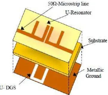
have the capability of suppressing undesired periodicity effect [6-17]. Multilayer-technique can be applied effectively to microwave circuits to minimize the structure size [15], thus the DGS adds an extra degree of freedom in microwave circuit design and opens the door to a wide range of application. The DGS can be designed in different geometries, depending on the application and on the desired frequency characteristics. The DGS structure similar to the one shown in Fig. 1, can be either a periodic or non-periodic cascaded configuration etched in the back side of a metallic ground plane of a planar transmission line. The introduction of the DGS structures, with similar frequency behavior as DMS, perturbs the current distribution in the ground plane. This disturbance leads to an important change in the electrical characteristics of the structure (capacitance and inductance). DGS (DMS) has a simple structure, which corresponds to an equivalent LC circuit model, such topology can be widely and potentially applicable in order to design compact RF circuit. To meet the requirements in modern wireless communication, much effort and publications have been made in other papers to develop a variety of compact band- and low pass filters with sharp and deep rejection outside the pass band region by generating transmission zeros or attenuation poles.
Fig. 1. Three-dimensional view of the U- cells.
In this paper, a novel WLAN band pass filter with the help of microstrip coupled U-DGS-resonators has been designed using the coupling matrix technique. The experimental results of the proposed band pass filter show compact size, good selectivity, high quality factor, and two transmission zeros above and below the pass band. The proposed filter is fabricated and measured. The measured results exhibit good agreement with the simulations.
II. CHARACTERISTICS OF U-RESONATOR
Fig. 2 (a) shows the schematic layout of the newly U-DGS resonator. It is etched in the ground plane and excited by a 50 line. The proposed U-DGS consists of two parallel capacitive arms, which are connected together via a rectangular shaped slot of 0.4 mm and 0.2 mm width, respectively. The slot channel corresponds to an inductance as shown in Fig. 2 (a). The circuit parameters can be extracted from an electromagnetic simulation by matching to a one pole Butterworth band stop filter response, as discussed in [18]. The width (w = 1.9 mm) of the feed strip line (50 ), placed on the top layer, has been calculated using TX-line program. All components are supported by a thin metal-backed substrate (Rogers RO3210) with a thickness of h = 0.813 mm, r = 3.38, and tan = 0.0023.
The U-resonator (see Fig. 2 (a), (b)) can be also modeled using a parallel LC circuit as shown in Fig. 3. The values of L and C are computed using,
(1)
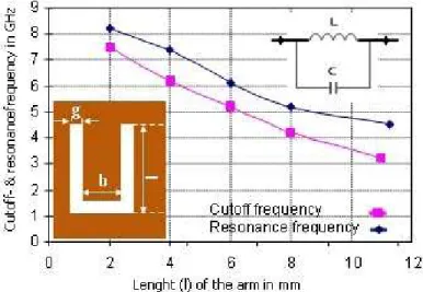
The values of the cut-off and resonance frequency fcand fp, respectively can be found from the transmission characteristics of the U-slot. As shown in Figs. 3 and 4, several experiments have been carried out in order to demonstrate the dependence of the DGS dimensions on the frequency positions. Two different DGS dimensions are first introduced for fine tuning of the resonance and cutoff frequency and precise realization of the circuit configuration. The tuning is realized only through a simple modification in the structure's size. To investigate this resonator size, the width of the DGS cell has been characterized with b and g and these values are set to 3 mm and 1 mm, respectively. The length l is adjusted from 2 mm to 11 mm. This led the |S21| characteristics of the resonance pole and
the cutoff frequency to vary from 4.5 GHz to 8.2 GHz and from 3 GHz to 7.5 GHz, respectively as shown in Fig. 3. When the length l of the DGS arm is increased, both frequency positions will be shifted to lower frequencies range, where the frequencies are changing fast.
(
)
C
(
f
)
nH
L
pF
f
f
f
C
p c p c 2 2 225
&
5
π
π
−
=
Fig. 2. Three-dimensional view of the DGS cell, (a) U-DGS-Slot (b) U-resonator.
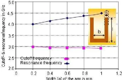
The effect of changing the width g for the DGS unit while keeping l constant causes a slight relocation in the resonance frequency. On the other hand, during this modification the cutoff frequency remains nearly constant [19]. This means that the change of the width g has no effect on the cutoff frequency. The effect of the width g on the resonance frequency position is shown in Fig. 4. Thus, the width, the resonance pole, and the cutoff frequency values vary from 200 µm to 1 mm, from 2.6 GHz to 4.5 GHz, and from 2.8 GHz to 3 GHz, respectively. The gap (g), which increases the attenuation pole, is shifted to higher frequencies indicating that g controls the effective capacitance. By employing the preview curves, it will be easy to design the required filters with desired resonance and cutoff characteristics.
Fig. 4. Comparison of resonance- and cutoff frequency of U-DGS cell versus the width g.
The DGS cell is simulated using Microwave Office. Simulation results are depicted in Fig. 4, which shows the characteristics of a one-pole band stop filter. Thus, one can get the attenuation pole frequency f0 at 4.5 GHz and the 3 dB cutoff frequency fc at 3 GHz for an arm length of 11 mm.
III. DESIGN PROCEDURE OF PLANAR CASCADED BAND PASS FILTER USING IDENTICAL U-DGS CELLS
In order to obtain WLAN three-pole microstrip band pass filter with two transmission zeros, low insertion loss in the pass band, and high selectivity, several structures were proposed. The included configurations use end-coupled slow-wave resonators and slow-wave open stub-tapped resonator filters. Two other techniques involve employing cross coupling and quasi-elliptic function filters, which are able to place the transmission zeros near the cutoff frequencies where higher selectivity with fewer resonators can be noticed. In all the previous works, the compactness factor was not satisfactory. One of the very successful topologies to achieve significant size reduction is to use coupled U-DGS components as shown in Fig. 1.
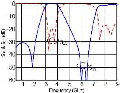
This topology can be used instead of edge coupled transmission /2 microstrip lines to design a compact band pass filter. As shown in Fig. 5, in order to widen the reject band and sharpen the transition from the pass band to the stop band, a new resonator topology is proposed. The filter structure consists of three magnetically coupled U-microstrip resonators, in which the right and left are connected with the 50 Ω feed lines. All neighboring identical U-resonators are located on the top layer and are separated from each other by a distance s of 0.5 mm, which is defined using empirical investigations. The filter is operated at frequency 3.6 GHz for WLAN application. The proposed structure was simulated using Roger RO4003 substrate with a dielectric constant of 3.38, substrate height of 0.813 mm, and thickness of 0.035 mm. Based on the simulation results, the filter is suitable for integration within various microwave subsystems. The band pass filter was designed to have two transmission zeros at 2 GHz and at 6 GHz. The simulation results are shown in Fig. 6.
Fig. 6. The simulation results of the conventional cascaded BPF.
As shown in Fig. 6, the insertion loss and return loss of the simulated results need further enhancement. Thus, in order to minimize the structure size and to also be able to improve the frequency characteristics of this band pass filter, another procedure so-called multilayer-technique will be used [20-22].
IV. DESIGN OF THE PROPOSED COMPACT BAND PASS FILTER
The multilayer-technique is used to improve the performance of the previous band pass filter. The new structure is similar to the original filter with simple modification; that involves removing the central microstrip resonator to be etched as a DGS-resonator in the ground plane, as shown in Fig. 7. Using this approach, the total area of this 3.4 GHz filter is reduced to 33% of its size. The compact band pass filter has the same bandwith (40%) but with improved pass band and stop band characteristics. In order to calculate the optimal coupling distances between both neighbored
0 1 2 3 4 5 6 7
resonators on the top layer, a coupling matrix method has been used. To be able to obtain the coupling matrix of the new topology, the specifications of the filter are defined and then the desired parameters are extracted using an optimization-based scheme [23]. The coupling coefficient and quality factor curves [24] are then used to realize the obtained coupling coefficients. In our case the third order filter is required to be designed to have a bandwidth BW = 1.5 GHz, return loss RL = 20 dB, and center frequency f0 = 3.7 GHz. The obtained coupling matrix from the optimization scheme is,
=
0.121 1.753 −1.550
1.753 0.213 1.753
−1.550 1.753 0.121
(2)
and the external quality factors are qin = qout = 9.315. The required fractional bandwidth FBW = BW/f0
= 0.405 is employed to realize the normalized coupling matrix and quality factors. The actual (de-normalized) coupling matrix becomes
M =
0.049 0.709 −0.627
0.709 0.086 0.709
−0.627 0.709 0.049
(3)
and Q1 = Q2 = 23, where M = FBW × m, and Q = q/ FBW. The calculated m-coupling coefficients
will be inserted in the experimental curve [25] in order to get the optimal distance between the microstrip resonators.
Fig. 7. Three-dimensional view of the new U-Band pass filter.
that the direct coupling is in this case, because of substrate thickness, is negligible compared to the cross-coupling between the upper neighbours U-resonators.
Fig. 8. The simulation results of the new proposed filter structure.
V. DESIGN AND FABRICATION OF THE IMPROVED BAND PASS FILTER
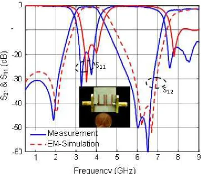
The proposed BPF with two U-DGS unit in the metallic ground plane and a U-microstrip resonator on the top layer with size of (20 × 15) mm2 is fabricated and measured using an HP8722D network analyzer as shown in Fig. 9. Fig. 10 shows the measured and the simulated results. A very good agreement between the simulated and measured results is observed. In the pass band, the measured insertion and return loss were less than 0.7 dB and 20 dB, respectively. The results shows significantly improved performance over the filters previously presented in [26-27].
Fig. 9. Photograph of the fabricated U-WLAN BPF.
frequency at 2.95 GHz, an insertion loss lower than 0.7 dB in the filter pass-band and, two transmission zeros appear close to the pass band at 2 GHz and 6 GHz. It can be seen from Fig. 10, that the fabricated filter (see Fig. 9) provides good performance in the stop band rejection and the pass-band insertion loss and smaller in size than those reported in literature.
Fig. 10. Measured and simulated S-parameters of the proposed BPF.
VI. HARMONIC SUPPRESSION USING DGS AND DMS
In order to avoid undesired characteristics in the previous filter, two procedures are proposed: 1- DGS technique.
2- DMS technique.
Using such technique [6] causes the slow wave effect property [7] and eliminates the undesired response in the determined frequency range. Based on our previous work [5-8], in our case, the rectangular- DGS unit is advantageous in comparison with dumbbell - or arrow-DGS shapes to solve this problem. It is shown in Fig. 11 with the following dimensions: x1 = 0.6 mm, x2 = 5 mm, y1 = 2.5
mm, y2 = 5 mm, w = 1.9 mm. The values were chosen to achieve resonance frequency around 2.75f0
Fig. 11. Layout of the DGS unit.
Fig. 12. The S-parameter results of the DGS-unit.
By using the DGS technique in the band pass filter as shown in Fig. 13, the center frequency of the new filter is compatible with the previous designed one as shown in Fig. 14. An improvement appears in the pass band attenuation (-30 dB). The second harmonic around 2.75f0 is suppressed. The coupling
Fig. 13. 3D-view of the proposed band pass filter with DGS-units.
The disadvantage in this method is a little distortion that appears in the left stop band. The dimensions of the used DGS-unit in the filter structure have been slightly modified compared to the proposed previous one in order to optimize the filter frequency response.
In order to obtain a filter with the optimum response, another technique named DMS (Defected Microstrip Structure) is applied as shown in Fig. 15. This technique has advantages versus that of the DGS. The former minimizes the radiation losses compared to the later, which leads to significant improvement in stop band attenuation. The second advantage is reducing the design and the manufacturing complexity. Introducing the DMS often adds a remarkable improvement in size of the filter.
Fig. 15. Layout of the DMS unit.
The DMS dimensions were chosen to obtain a resonance frequency in the region of the undesired harmonic as shown in Fig. 16. The values of the dimensions are as follows: x1 = 1 mm, x2 = 11 mm,
y1 = 0.6 mm, y2 = 0.4 mm. To apply this technique, two identical defects are etched into microstrip
feed lines near from the input and output of the structure.
The topology of the new DMS filter as shown in Fig. 17 was easily designed and controlled with neglecting the coupling that can negatively affect filter response. As shown in Fig. 18, the symmetry of the filter’s behavior was improved with highly accepted pass band losses and stop band attenuations.
Fig. 17. 3D-view of the new band pass filter with DMS-units.
VII. DESIGN OF CLASSICAL THIRD ORDER CASCADED LOW PASS FILTER USING U-RESONATORS
The Bandpass filter is composed of two cascaded LC resonators (two DGSs) and a gap
(J-admittance inverter), which composed of one series capacitor (C
s) and two shunt capacitors
(C
p) ( -Form). The closing of the gap using a microstrip line leads to a transformation of BPF
circuit to LPF circuit, which is composed of two cascaded DGS-Resonators and a shunt
capacitor 2(C
p).
Fig. 19 illustrates the geometry of the proposed LPF. The filter consists of threemagnetically coupled U-DGS resonators, in which the first and the third are connected with the 50 Ω feed lines. The U-DGS resonators are located on the top layer. The three microstrip resonators are identical and are separated from each other by a distance s of 0.5 mm.
Fig. 19. Layout of the Low pass filter.
The filter was simulated for a Rogers RO4003 substrate with a relative dielectric constant of r =
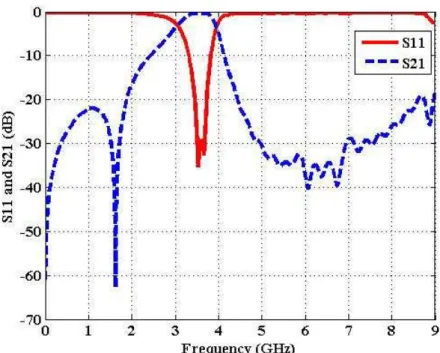
3.38 and a thickness of h = 0.813 mm. The simulation results of the lowpass filter are shown in Fig. 20.
One can notice from the S11 results of Fig. 20 that the pass-band region is at an average level of -14
dB, while the rejection band for the LPF starts at 4 GHz as represented by the S21 data. The filter was
designed to have a cutoff frequency of fc = 3.7 GHz.
VIII. UNDERSTANDING OF FREQUENCY BEHAVIORS THROUGH ELECTROMAGNETIC FIELD DISTRIBUTION
To verify the stability of the performance of the proposed LPF DGS structure, the near field distribution has been computed as shown in Fig. 21. The magnetic field was computed at two frequencies in the pass-band and stop-band regions. It can be clearly noticed that at 1.5 GHz, the magnetic field is almost concentrated around of the inferior region (i) between the arms of the U-microstrip slots and along of the U-microstrip capacitor (cannel line) (ii). It is obvious that the field reaches the maximum distribution at the first two U-shaped cells and slightly decreases when approaching the third cell. This conclusion triggers the idea of investigating the multilayer technique and its effect on the filter performance when one can minimize the filter dimensions.
On the other hand, the magnetic field can be shown at the frequency of 5 GHz, because of the microstrip capacitors, with a high concentration around port 1 and no energy flow around port 2. This asymmetric filed distribution along the U slots presents the stop-band behavior.
IX. IMPROVEMENT OF THE COMPACTNESS OF THE LOW PASS STRUCTURE USING MULTILAYER TECHNIQUE
In order to minimize the size of the proposed prototype LPF, the multilayer technique was induced [21]. A size reduction was achieved by placing one of the U-shaped cells on the top layer of the substrate to be etched in the ground plane. A total size reduction of 33 % was gained, and the new total dimension of the dielectric substrate became (20 × 15) mm2, as described in Fig. 22. Fig. 22 shows the schematic diagram of the multilayer LPF, representing the dimensions of both, top and bottom layers. The results of the proposed multilayer LPF generated using Microwave OfficeTM [28] were compared to those generated using Ansoft HFSSTM [29]. The scattering parameters frequency response results are shown in Fig. 23. Good agreement between both results can be observed. Based on the simulated results one can realize that the proposed multilayer LPF has better performance in the pass band region; having less than 20 dB through the entire region when compared to the conventional LPF shown in Fig. 20.
Fig. 23. Comparison between the simulation results of the compact low pass filter using Microwave OfficeTM and HFSSTM.
X. ELECTROMAGNETIC FIELD DISTRIBUTION ALONG ON THE PROPOSED LOW PASS FILTER
Fig. 24. Electromagnetic field distribution results in the LPF. (a) pass-band at 2 GHz and (b) reject band at 6 GHz.
XI. CONCLUSION
ACKNOWLEDGMENT
The authors would like to thank the German Research Foundation (DFG) for financial support of this project. The authors are grateful to Mr. Harald Dempewolf and Mr. Dennis Winkler for their supports and assistances for their cooperation in laboratory.
REFERENCES
[1] Zhang, X. Y. and Q. Xue, “Novel centrally loaded resonators and their applications to bandpass filters,” IEEE Trans. Microw. Theory Tech., vol. 56, no. 4, pp. 913–921, Apr. 2008.
[2] Kuo, J. T. and W. Hsu, “Parallel coupled microstrip filters with suppression of harmonic response,” IEEE MicrowaveWireless Comp. Lett., vol. 12, pp. 383–385, Oct. 2002.
[3] Hong, J. S. and M. J. Lancaster, “Cross-coupled microstrip hairpin-resonator filters”, IEEE Trans. Microwave Theory Tech., vol. 46, no. 1, pp. 118-122, Jan. 1998.
[4] Awida, M., A. Boutejdar, A. Safwat, H. El-Hennawy, A. Omar, “ Multi-bandpass filters using multi-armed open loop resonators with direct feed,” IEEE MTT-S International Microwave Symposium, Honolulu, Hawaii, June 03 - 08, 2007. [5] Hsieh, L. H. and K. Chang, “Compact low pass filter using stepped impedance hairpin resonator,” Electron Lett., vol.
37, pp. 899–900, (2001).
[6] Boutejdar, A. and A. Omar, “Compensating For DGS Filter Loss,” Microwave & RF Journal [Design Features], Issue 2, pp. 68-76, February. 2012.
[7] Boutejdar, A., S. Amari, and A. Omar, “A Novel Compact J-Admittance Inverter-Coupled Microstrip Bandpass Filter Using Arrowhead-Shape As Defected Ground Structure (DGS),” Microwave and Optical Technology Letters , vol. 52, Issue 1, pp: 34- 38, January 2010.
[8] Abdel-Rahman, A., A. K. Verma, A. Boutejdar, and A. S. Omar, “Control of band-stop response of Hi-Lo microstrip low-pass filter using slot in ground plane”, IEEE Trans. on Microwave Theory and Tech., vol. 52, pp. 1008 – 1013, Mar. 2004.
[9] Yang, Y. Y., R. C. Qian., and T. Itoh, “A novel low loss slow-wave microstrip structure”, IEEE IEEE Microwave Guide Wave Lett., vol. 47, no. 8, pp. 372 – 374, 1998.
[10]Garde, L., M. J. Yabar, and C. D. Rio, “Simple modeling of DGS to design 1D-PBG low pass filter,” Microw. Opt Technol. Lett., vol. 37, no. 3, pp. 228–232, May 2003.
[11]Ahn, D., J. S. Park, C. S. Kim, Y. Qian, and T. Itoh, “A design of the low-pass filter using the novel microstrip defected ground structure,” IEEE Trans. Microwave Theory Tech., vol. 49, pp. 86–93, Jan. 2001.
[12]Boutejdar, A. “An Improvement of Defected Ground Structure Lowpass/Bandpass Filters Using H-Slot Resonators and Coupling Matrix Method”, Journal of Microwaves, Optoelectronics and Electromagnetic Applications, vol. 10, Issue 2, pp. 295-307, ISSN 2179-1074, December 2011.
[13]Kim, C. S., J. S. Lim, S. Nam, K. Y. Kang, and D. Ahn, “Equivalent circuit modeling of spiral defected ground structure for microstrip line,” Electron. Lett., vol. 38, no. 19, pp. 1109–1120, 2002.
[14]Al Sharkawy, M., A. Boutejdar, D. Abd El Aziz, and E. Galal, “Design Of Compact Microstrip Filter With Large Reject Band Using A New Multi-Sections T-Shaped Defected Ground Structure and Multilayer Technique”,
Microwave and Optical Technology Letters, vol. 53, isuue 04, pp. 35-39, May 2011.
[15]Kim, J. P. and W. S. Park, “Microstrip Low Pass Filter with Multislots on Ground Plane,” Electronics Letters, vol. 37, no. 25, December 2001.
[16]Park, J. S., H. S. Yun, and D. Ahn, “A design of the novel coupled line bandpass filter using defected ground structure with wide stopband performance,” IEEE Trans. Microw. Theory Tech., vol. 50, no. 9, pp. 2037–2043, Sep. 2002. [17]Boutejdar, A., A. Elsherbini, and A. S. Omar, “Method for widening the reject-band in low-pass/band-pass filters by
employing coupled C-shaped defected ground structure”, IET Microwaves Antennas & Propagation, vol. 2, Issue 8, pp. 759-765, Dec 2008.
[18]Kim, C., J. S. Park, A. Dal, and J. Kim, “A novel 1-D periodic defected ground structure for planar circuits,” IEEE Microwave Guided Wave Lett., vol. 10, pp. 131–133, Apr. 2000.
[19]Boutejdar, A. et al., “Improvement of microstrip low pass filters' characteristics using an optimized number of new multi-ring defected ground structures”, Microwave and Optical Technology Letters, vol. 49 Issue 12, pp. 3074-3078, Dec. 2007.
[20]Boutejdar, A., A. Batmanov, A. Elsherbini, A. S. Omar, and E. P. Burte, “A Miniature 3.1-GHz Microstrip Bandpass Filter with A Suppression of Spurious Harmonic Using Multilayer-Technique and Defected Ground Structure Open Loop-Ring (DGS)”, Proc. EUROEM European Electromagnetic 2008, Lausanne, Switzerland, 21-25 July 2008. [21]Boutejdar, A., A. Omar, E. P. Burte, R. Mikuta, and A. Batmanov, “DGS and Multilayer Methods Make LPF”,
Microwave & RF Journal[Design Features], pp. 61-72, issue March/April. 2011.
[22]Boutejdar, A., A. Omar, E. P. Burte and R. Mikuta, “ Design of Compact Ultra-Wide Stopband Lowpass Filter Using a U-Slotted Ground Structure (SGS) and Multilayer-Technique”, Recent Patents on Electrical Engineering journal, Bentham Science Publishers, ISSN: 1874-4761, vol. 4, issue 2, pp: 139-144, May 2011.
[23]Cameron, R. J. “General coupling matrix synthesis method for Chebyshev filtering functions,” IEEE Transactions On Microwave Theory And Techniques, vol. 47, No. 4, April 1999.
[25]Boutejdar, A., A. Elsherbini, A. Balalem, J. Machac, and A. Omar, “Design of new DGS hairpain microstrip bandpass filter using coupling matrix method,” PIERS Progress in Electromagnetics Research Symposium, Prague, Czech Republic, pp. 261-265, August 27 - 30, 2007.
[26]Abdel-Rahman, A., A. K. Verma, A. Boutejdar, and A. S. Omar, “Compact stub type microstrip bandpass filter using defected ground plane”, IEEE Microwave and Wireless Components Letters, vol. 14, pp.136-138, 2004.
[27]Boutejdar, A., A. Elsherbini, and A. Omar, “Improvement of bassband and sharpness factor of parallel coupled microstrip bandpass filters using discontinuities correction,” Mediterranea Microwave Symposium, Budapest, pp. 121-124, 2007.

