А -Е Е Е А Ы Е , Е А
я варь–февра ь 2017 17№ 1 ISSN 2226-1494 http://ntv.ifmo.ru/ SCIENTIFIC AND TECHNICAL JOURNAL OF INFORMATION TECHNOLOGIES, MECHANICS AND OPTICS January–February 2017 Vol. 17 No 1 ISSN 2226-1494 http://ntv.ifmo.ru/en
NANOSCALE STRUCTURES GENERATION WITHIN THE SURFACE LAYER
OF METALS WITH SHORT UV LASER PULSES
D.S. Ivanova,b,c, A. Blumensteind,a, B. Rethfeldb, V.P. Veikoc, E.B. Yakovlevc,M.E. Garciaa
a
University of Kassel, Kassel, 34132, Germany
b
Technical University of Kaiserslautern, Kaiserslautern, 67663, Germany
c
ITMO University, Saint Petersburg, 197101, Russian Federation
d
Laser-Laboratorium-Göttingen e.V., Göttingen, 37077, Germany Corresponding author: [email protected]
Article info
Received 16.10.16, accepted 10.12.16 doi: 10.17586/2226-1494-2017-17-1-1-15 Article in English
For citation: Ivanov D.S., Blumenstein A., Rethfeld B., Veiko V.P., Yakovlev E.B., Garcia M.E. Nanoscale structures generation within the
surface layer of metals with short UV laser pulses. Scientific and Technical Journal of Information Technologies, Mechanics and Optics, 2017, vol. 17, no. 1, pp. 1–15. doi: 10.17586/2226-1494-2017-17-1-1-15
Abstract
We have completed modeling of a laser pulse influence on a gold target. We have applied a hybrid atomistic-continuum model to analyze the physical mechanisms responsible for the process of nanostructuring. The model combines the advantages of Molecular Dynamics and Two Temperature Model. We have carried out a direct comparison of the modeling results and experimental data on nano-modification due to a single ps laser pulse at the energy densities significantly exceeding the melting threshold. The experimental data is obtained due to a laser pulse irradiation at the wavelength of 248 nm and duration of 1.6 ps. The mask projection (diffraction grating) creates the sinusoidal intensity distribution on a gold surface with periods of 270 nm, 350 nm, and 500 nm. The experimental data and modeling results have demonstrated a good match subject to complex interrelations between a fast material response to the laser excitation, generation of crystal defects, phase transitions and hydrodynamic motion of matter under condition of strong laser-induced non-equilibrium. The performed work confirms the proposed approach as a powerful tool for revealing the physical mechanisms underlying the process of nanostructuring of metal surfaces. Detailed understanding of the dynamics of these processes gives the possibility for designing the topology of functional surfaces on nano- and micro-scales.
Keywords
UV laser pulses, nanostructuring, simulations, molecular dynamics Acknowledgements
The reported study was supported partially by the Ministry of Education and Science of Russia, research agreement No.14.578.21.0197 (RFMEFI57816X0197, by RFBR grant No. 14-29-07227 OFI-M, and the Government of the Russian Federation Grant No. 074-U01, and DFG grants IV 122/1-1 IV 122/1-2.
ɍȾɄ 538.913, 53.01, 519.6
ɈȻɊȺɁɈȼȺɇɂȿ
ɇȺɇɈɊȺɁɆȿɊɇɕɏ
ɋɌɊɍɄɌɍɊ
ȼ
ɉɊɂɉɈȼȿɊɏɇɈɋɌɇɈɆ
ɋɅɈȿ
ɆȿɌȺɅɅɈȼ
ɉɊɂ
ȼɈɁȾȿɃɋɌȼɂɂ
ɍɅɖɌɊȺɄɈɊɈɌɄɈȽɈ
ɅȺɁȿɊɇɈȽɈ
ɂɆɉɍɅɖɋȺ
ɍɅɖɌɊȺɎɂɈɅȿɌɈȼɈȽɈ
ȾɂȺɉȺɁɈɇȺ
Ⱦ.ɋ. ɂɜɚɧɨɜa,b,c, Ⱥ. Ȼɥɸɦɟɧɲɬɚɣɧd,a, Ȼ. Ɋɟɬɮɟɥɶɞb, ȼ.ɉ. ȼɟɣɤɨc, ȿ.Ȼ. əɤɨɜɥɟɜc, Ɇ.ɗ. Ƚɚɪɫɢɹa
a
, , 34132,
b , , 67663,
c И
, - , 197101,
d ё , ё , 37077,
ɂɧɮɨɪɦɚɰɢɹ ɨ ɫɬɚɬɶɟ
16.10.16, 10.12.16 doi: 10.17586/2226-1494-2017-17-1-1-15
–
ɋɫɵɥɤɚ ɞɥɹ ɰɢɬɢɪɨɜɚɧɢɹ: И . ., ., ., . ., . ., . .
// - , . 2017. . 17. № 1.
Ⱥɧɧɨɬɚɰɢɹ
.
, ( )
, , .
,
.
248 1,6 . ( )
500 .
, ,
, . ,
.
- .
Ʉɥɸɱɟɜɵɟɫɥɨɜɚ
, , ,
Ȼɥɚɝɨɞɚɪɧɨɫɬɢ
, №14.578.21.0197 (RFMEFI57816X0197), И № 14-29-07227 И- ,
№ 074-U01 DFG IV 122/1-1 IV 122/1-2.
Introduction
The growth of ultrashort pulse laser technologies has opened up new opportunities for high-precision processing of a wide range of materials, including dielectrics, semiconductors, and metals, thus, enabling numerous practical applications in the fields ranging from micromachining to photonics and life sciences [1–3]. The ability of ultrashort lasers to deposit energy into a much localized volume of the irradiated target makes it possible to perform very selective material modification and, at the same time, provides unique opportunities for investigating material behavior and properties under extreme conditions of strong electronic excitation, rapid heating and cooling, and ultrafast laser-induced mechanical deformation. This can result in the formation of unique structures in a pre-surface layer of a material affected by the laser deposition [1–3].
The initial non-thermal material response to the ultrafast laser excitation is quick, within picoseconds, followed by the onset of thermal processes induced by the energy transfer from the excited electrons to atomic vibrations, commonly described as electron-phonon coupling. The rapid electron-phonon equilibration can
produce ultrafast heating rates exceeding 1014 K/s, providing, therefore, opportunities for investigation of the
kinetic limits of achievable superheating of solid phases. Indeed, a combination of time-resolved optical, X-ray and electron diffraction probing of short pulse laser melting [4–6] with theoretical analysis and Molecular
Dynamics (MD) simulations[7, 8] has provided important information on the time-scales and mechanisms of the
melting process occurring under conditions of strong superheating. However, the short pulse laser irradiation may cause not only the rapid heating and melting of localized surface or internal regions of the target, but also produce sharp temperature gradients leading to a rapid quenching of the transiently melted material. In strongly absorbing materials, such as metals or semiconductors, a combination of shallow depth of the laser energy deposition with high thermal conductivity of the irradiated material can lead to cooling rates approaching
1012 K/s. The cooling rates can be even higher, in excess of 1013 K/s [9], when the laser energy deposition is
confined not only within the thin surface layer of the irradiated target but also in the lateral dimensions, creating conditions for even faster two- or three-dimensional heat transfer from the absorption region. The laterally localized laser energy deposition can be achieved by using tightly focused laser beams [10–11] or taking advantage of the local field enhancement in the vicinity of a tip of a scanning probe microscope [12, 13]. Since the number of highly non-equilibrium interrelated processes above can be involved into the material response to a short laser pulse irradiation and since those processes can take place on a wide spatial and time scales, it can be difficult, or sometimes impossible, to treat the obtained experimental data with a definite confidence.
In this context, due to its microscopic approach, the MD-based modeling was found to be an efficient
numerical tool for the theoretical investigation of ultrafast non-equilibrium laser induced processes in materials. Recently, with the combined atomistic-continuum model [14], the kinetics of the induced phase transition processes is addressed at an atomic level with the MD method. At the same time, the processes of laser light absorption by conduction band electrons, fast electron-heat conduction, and generated strong electron-phonon non-equilibrium are described in the continuum with the help of the Two Temperature Model (TTM) [15]. This combined atomistic-continuum MD-TTM model [14] was successfully used in studying short pulse laser induced melting, spallation, and ablation of thin and thick metal targets [16–18].
just above the damage threshold. In the present work, however, the applied incident fluences ranged from near to
significantly above the damage threshold valuing of 125, 160, and 250 mJ/cm2. Experiments and simulations are
executed with the same spatial laser intensity period of 270 nm. The spatial irradiation geometry of the experiment combined with a properly selected model volume gives the opportunity to obtain a direct comparison of experiment and simulation of nanostructuring of a thick Au target.
To obtain smaller structures, the use of ultrashort UV pulses instead of visible light pulses is advantageous since the shorter wavelength allows a far better spatial resolution. Meanwhile, the use of pulse length shorter than the characteristic electron-phonon relaxation time of the material (about 25 ps for gold at the fluencies near the melting threshold [21, 22]) allows for a complete deposition of the pulse energy in the electronic system before transferring it to the lattice, thus ensuring highly localized material modifications [23]. For the generation of deterministic sub-micron periodic patterns various irradiation concepts have been demonstrated. The required interference of two or more beams has been accomplished by mask projection [24], a two grating interferometer [25], or a proximity phase mask set-up [26]. A wide range of applications through optimized light coupling in photovoltaic [27], Light Emitting Diodes (LED) [28], and detector devices [29] can benefit from the gained knowledge and allow a detailed control of the fabrication process of next generation devices.
The Experiment
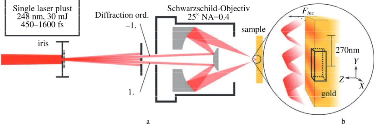
Similarly to [19, 20], all surface structuring experiments are accomplished by single pulse exposure using a combination of interference and mask projection to form a large area sinusoidal intensity distribution on the sample surface (Fig. 1). The applied two-beam interference (resulting in the sinusoidal pattern) allows reaching the highest possible spatial intensity gradient, crucial for keeping the simulated volume as small as possible. The
smallest available modulation period d is then only limited by the numerical aperture (NA) of the applied optics
and the laser wavelength and can be expressed as d = /2NA. Thus, using a short wavelength of 248 nm and a
large numerical aperture of NA = 0.4, a lower limit for the periodicity of approximately 270 nm is obtained (as compared to our previous experiments 310 nm). The used laser system consists of a frequency tripled Ti:Sa system seeding a KrF excimer amplifier producing pulse energies of up to 30 mJ at a wavelength of 248 nm and a repetition rate of 10 Hz. The pulse length of 1.6 ps is measured by using a frequency resolved optical gating (FROG) trace obtained with a device described in [30]. Single pulses are selected by a shutter. The used pulse energy is set by a variable attenuator. The flat top central part of the laser beam illuminates the mask comprising a circular aperture of 1 mm diameter in contact with a Cr-on-quartz grating of lines and spaces with 25 µm period and duty cycle 0.5. The demagnification of the Schwarzschild-objective used for mask imaging is
adjusted to be 25×. Consequently, the diameter of the overall projected area on the workpiece is 40 µm. Since all
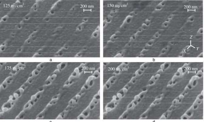
diffracted orders emerging from the transmission grating except the two first orders are blocked, the image is formed via two-beam interference, resulting in a sinusoidal intensity distribution across the 40 µm area. A schematic view of this distribution is shown in Fig. 1, b. The resulting structures, obtained with the experimental set-up described above, can be seen as Scanning Electron Microscopy (SEM) images in Fig. 2 for different incident fluences. The presented images reveal the periodic frozen structures with difference aspect ratio depending on the applied fluence. One can also see that with the increase of fluence, the number of opened voids to the surface grows as well. The mechanism of these periodic structures formation, generation and evolution of voids, and the microstructures character will be investigated with an advance theoretical approach described below in the next section.
a b
Fig. 1. Mask projection setup for a periodic surface structuring of an area of 40 µm. A sinusoidal interference pattern with a period of 270 nm is obtained by using only the ± 1st diffraction orders (a). Schematic shape of the incident fluence distribution (Finc) created by an ideal single laser pulse self-interference of two beams
under a certain angle (b)
270nm
Y
Z X Finc
sample Diffraction ord.
–1.
1. iris
Schwarzschild-Objectiv
25NA=0.4
Single laser plust 248 nm, 30 mJ
a b
c d
Fig. 2.SEM pictures showing surface modifications from a single laser pulse with periodic line spacing of 270 nm corresponding to the periodic irradiation pattern created by two beam interference for the incident fluences of 125 mJ/cm2 (a), 150 mJ/cm2 (b), 175 mJ/cm2 (c), and 200 mJ/cm2 (d). Small segments of a larger structured
area on a thick gold sample at four different average incident fluences are shown. The sample was tilted in the SEM by 45° relative to the electron beam axis to increase the contrast
The Model
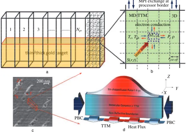
The essential concepts and applications of the combined atomistic-continuum model MD-TTM to study the evolution of metallic solids excited by an ultrashort laser pulse are described in details in [14]. The model consists of two parts: the atomic motion is described within the MD approach, whereas a diffusion differential equation for electrons is accounting for the effect of free carriers via their temperature dynamics (see Eqs. 3 and 4 in [14]). Thus, the combined model provides a detailed atomic-level description of the kinetics of fast non-equilibrium processes, of laser melting with atomic resolution and, at the same time, in continuum ensures for the adequate description of the laser light absorption by conduction band electrons, the energy transfer to the lattice due to electron-phonon coupling, and the fast electron heat conduction (see Fig. 2 in [14]). Based on the atomistic-continuum approach, the MD-TTM model was further developed for the simulation of nanostructuring processes of metal targets in a multiprocessing algorithm (running in parallel) to be applied in large scale modeling tasks. For the case of modeling nanostructuring of thick metal targets with an UV laser pulse on the experimental scale the model is in details in [19, 20], whereas its successful applications for the case of thin targets can be found elsewhere [31, 32].
The schematic view of the total computational cell utilized in the simulation of the nanostructuring process can be seen in Fig. 3. The idea of modeling on the experimental scale is based on symmetry utilization of
the experiment described above, see Figs. 1 and 2. The laser beam, sinusoidally shaped in one dimension (Y),
leaves a uniform laser intensity distribution in X direction. Dealing with the size of the laser spot of about 40 m
in diameter (flat top in X and sinusoidal shaped in Y), its central part will therefore not be affected by a diffusion
process in X direction up to the order of 1 s of the experimental time. This estimated time is confirmed in
preliminary calculations using the TTM approach [15]. Considering this time as long enough for the formation and solidification of the nanostructures [32], this provides a possibility for Periodic Boundary (PB) conditions in
X during our simulation time (up to several ns). As a result, since we do not expect any temperature and pressure
gradients in the lateral direction parallel to the grating lines (X), for a simulation allowing for identical
comparison with experiment, we constructed the computational cell as schematically shown in Fig. 5. The Au
MD supercell consisting of 160,000,000 atoms was taken with dimensions of (40×270×200) nm in X, Y, and Z
directions respectively. In order to avoid unnecessary and expensive MD integrations in deep bulk of the
material, at a certain depth from the surface (in Z direction) we impose Non Reflective Boundary (NRB)
conditions. Demanded by the investigated physics, the MD-TTM model was applied only above that limit. The NRB conditions were described in [33] and modified in [32] for the case of a nanostructuring experiment. The NRB conditions, however, are transparent for the heat flux, and the ordinary TTM model was solved beyond the
125 mj/cm2 200 nm 150 mj/cm2 200 nm
Z
Y X
200 nm
NRB taking the electron and phonon temperature dynamics into account on a scale up to 50 µm away from the irradiated surface. Thus, with the described computational cell we simulate a thick Au target with atomic resolution within 200 nm from the surface in the assumption that no phase transition would take place beyond the NRB. This assumption was verified in all our simulations.
The characteristic size of liquid nuclei forming during the laser-induced phase transition process and their initial evolution in the development of the liquid phase has been determined in our previous works to be of the
order of 10 nm [18, 31, 32]. For the applied fluence regime therefore, we consider the width of 40 nm in X for
the slice of modeled material big enough for a safe application of the PB conditions in that direction. A Free Boundary (FB) is imposed at the top, where the material is irradiated with a laser pulse. Finally, we impose PB in
Y direction with the size of MD-TTM domain equal to the period of the sinusoidal pulse shape. In essence, it
does not matter where the pulse is centered with respect to the MD domain in Y direction. For convenience, we
adjust the maximum peak of the laser intensity to the central point of the sample in Y direction. The subsequent
multiple translation of this distribution in X and Y direction will reproduce the intensity profile as it is given by
the experimental setup, see Fig. 1.
Fig. 3. Schematic representation of the total computational cell divided to the number of processors Nproc (256 in this modeling in Y direction) with utilization of the Message Passing Interface (MPI) library (a). In each processor geometry, a combined atomistic-continuum model MD-TTM was realized in 3D-space (based on cut-off distance of the interatomic potential rcut-off) subject to find the temperatures of electrons Te and phonons
Tph, pressure P, and density ρ for a given laser source S(r,t), where r is the position in space and t is time. The energy exchange between electrons and phonons ∆Ee-phis accounted for in the model each MD time step. (b). SEM picture (Fig. 2, a) of periodic nanostructures on Au (c) and schematic representation of the computational cell used in the super large scale modeling of this process on the experimental scale (d). PB are the periodic
boundaries. The non-reflective boundaries are transparent for the heat fluxes
The MD-TTM domain was divided into a 3D mesh with nm3 unit cell and the thermo-physical properties
of the atomic subsystem (such as temperature and pressure) were averaged over the closest 26 neighboring cells (that totally accounts for about 2,500 atoms) to suppress their value fluctuations due to MD noise [14, 32]. The choice of the mesh size is justified, on one hand, by its minimization for the efficient neighbor list search and calculations of forces in the MD part. On the other hand, the cell must be big enough to accommodate a group of atoms large enough to introduce their statistical description (under assumption of quasi-equilibrium) for a reliable determination of their macroscopic quantities.
In order to have a possibility for the direct comparison of simulation with experiment, the MD-TTM model has implemented a realistic interatomic potential. For this purpose, we choose the Embedded Atom Method (EAM) implementing the interatomic potential by Zhakhovskii et al. [34], optimized for Au. For an
1 2 3 Npr
MPI exchange at processor border
3D MD-TTM
electron conduction
Te, Tph P,
S(r,t) rcut-off
Ee-ph
Z
X Y
Y Z
X
200 nm
PBC
TTM Heat Flux PBC
a b
equilibrium crystal at P = 0 GPa and T = 0 K the potential gives –367.609 kJ/mol for the cohesive energy, 179.4 GPa for the bulk modulus, and 0.4065 nm for the lattice constant. Furthermore, this potential represents the experimental thermophysical properties of the modeled material (such as equilibrium melting temperature, heat capacity, volume of melting, and linear thermal expansion coefficient) with an accuracy of more than 99.5% [35]. A more detailed description of the model used to describe periodic nanostructuring of metals with UV laser pulse can be found elsewhere [19, 20].
Finally, the computational supercell setup, schematically shown in Fig. 3, was run across 256 processors for 30 days resulting in a simulated experimental time of up to 1000 ps of the nanostructuring process for three
different applied incident fluences of 125, 160, and 250 mJ/cm2. In order to perform such a super large-scale
simulation, the MPI (Message Passing Interface library) version of the atomistic-continuum model MD-TTM
was adopted, optimized, and used as described in [32]. The processors space geometry 1×256×1 along the X, Y,
and Z axes was chosen correspondingly for a better load balance during the whole simulation. This choice is
governed by our expectation that the laser-assisted material expansion process will proceed upwards and the number of atoms to be processed by each processor therefore will roughly stay the same.
Results and Discussions
In general, the mechanism responsible for the nanostructuring process is similar to that described in [31] with a simplified model and later confirmed in a super large scale modeling of nanostructuring of thin [32] and thick metal targets [19, 20]. Namely, the relaxation of the laser-induced compressive stresses generated under conditions of the inertial stress confinement [16, 36] serves as the main driving force responsible for the acceleration of a transiently melted region of the target with subsequent bloating of a nanostructure. Fast electron heat conduction, on the other hand, proceeding by two- or three-dimensional mechanism (depending on the experimental geometry), results in the electron temperature falling significantly below the temperature of atoms in the molten volume. In this case, the electrons, due to electron-phonon energy exchange, provide the conditions for the fast cooling of melted material and rapid solidification of a surface feature generated in the process of hydrodynamic motion of the liquid material.
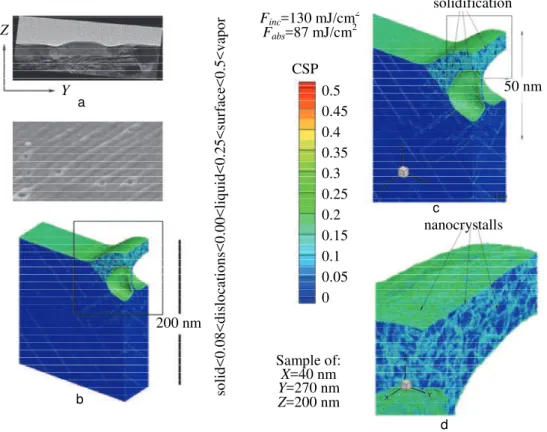
Fig. 4. SEM images of the 270 nm periodic structures (a) with the incident fluence Finc of 130 mJ/cm2 (corresponding to the absorbed fluence Fabs of 87 mJ/cm) are directly compared with the result of an atomistic simulation of the nanostructuring process (b). The atoms are colored with Central Symmetry Parameter (CSP) for
distinguishing the atoms with local order (solid – dark blue) from those of disordered structures (grain boundaries – blue, liquid – light blue, surface green, and vapor – red). The magnified view of the final
internal microstructure is shown in (c) and (d)
The snapshots of atomic configurations, shown in Fig. 4, reveal the formation of dislocation planes during the simulations in {1,1,1} directions. Being deviated too much from a perfect Face Center Cubic (FCC) crystalline structure, those atoms, characterized by a higher Central Symmetry Parameter (CSP), appear in light
Z
Y
a
Finc=130 mJ/cm2
Fabs=87 mJ/cm
2
solidification
nanocrystalls 50 nm
200 nm
b
c
d
Sample of:
X=40 nm
Y=270 nm
Z=200 nm
CSP 0.5 0.45 0.4 0.35 0.3 0.25 0.2 0.15 0.1 0.05 0
so
lid<0.
08<dis
lo
cations
<0
.0
0
<
liqu
id<0.2
5
<surface<0.5<va
blue color, still possess a higher order than that in a liquid, shown by blue color. One can conclude that as a result of thermal expansion of the material in response to the fast laser heating, a number of dislocation planes is induced and propagate in the directions with the lowest energy {1,1,1} and eventually form stacking faults. The generated stacking faults have a higher energy barrier for further dislocation planes propagation and stop them as a result. In fact, such a stacking fault organization would reinforce the material, working similarly to that described in short pulse laser peening experiments on steel [37–39] and theoretically studied in semiconductor solids [40].
The resulting snapshots presented in Fig. 5 also illustrate a complex interplay of fast laser melting, rapid cooling, resolidification, and relaxation dynamics of laser-induced stresses in the surface region of a gold target
during the nanostructuring process at the incident fluence of 160 mJ/cm2. The monocrystalline layer with
ultrafine grains (with the size of less than 5 nm) is produced by massive homogeneous nucleation of a solid
phase triggered by a deep undercooling of the melted surface region down to below than 0.7Tm (below 1000 K)
and features random crystallographic orientation of nanograins. The enlarged atomic-scale views of the surface microstructure are shown in Fig. 4 and Fig. 5 reveals a high density of stacking faults and nanograins. Because of the higher fluence as compared to that used in Fig. 4, the internal structure includes a number of solidified features inside of the hollow surface nanobarrier. The formation of similar structural elements has also been observed in frozen nano-spikes generated in the spallation regime, in recent MD simulation by Zhigilei et al [41].
Fig. 5.Atomistic snapshots taken at the end of modeling at t = 1000 ps and obtained in simulation of the periodic nanostructuring process of thick Au target at the incident fluence of 160 mJ/cm2. Similarly to that of Fig. 4, the atoms are colored according to CSP value. A detailed view on the microscopic structure of the internal
structures can be seen in magnified boxes
The computational prediction of the formation of a thin nanocrystalline layer with high density of grains suggests the short pulse laser processing as a viable alternative to the severe plastic deformation [42] or pulsed electrodeposition [43] techniques that are currently employed to yield the maximum structural refinement and high strength of metal samples. Moreover, the localization of the nanocrystalline layer within a thin surface layer (up to about 50 nm deep) of the target and the prominent presence of grain boundaries are two factors that may also increase the ductility of the laser-modified layer [44–46], a property that is generally incompatible with high strength.
As already mentioned above, the fast rate of energy deposition by short laser pulses may lead to the generation of compressive stresses. The laser-generated stresses are particularly high in the regime of stress
confinement [16, 36], when the time of the laser heating (defined by the laser pulse duration, τp, or the time of
the electron-phonon equilibration, τe–ph, whichever is longer) is shorter than the time required for the mechanical
relaxation (expansion) of the heated volume, i.e., max{τp, τe–ph} ≤Lp/Cs, where Cs is the speed of sound in the
target material and Lp is the effective depth of the laser energy deposition (optical penetration depth or, in the
case of metals, the depth of diffusive/ballistic energy transport during the time of the electron-phonon equilibration). The latter can be a function of electron heat conductivity and for the same pulse duration can
significantly alter the value of Lp depending on the applied fluence [47].
The case of onset of the spallation regime during the nanostructuring process is depicted in Fig. 6 as a
sequence of snapshots taken from the simulation with the applied fluence of 250 mJ/cm2. The relaxation of the
laser-induced stresses formed in the material under conditions of inertial stress confinement [16, 36] induces strong tensile stresses (about –4GPa) that in the liquid part of the material exceed the material strength (the atmospheric pressure, on the order of 0.1MPa is a negligible contribution here) and promotes the formation of
CSP 0 0.1 0.2 0.3 0.4 0.5
5 nm
Finc=160 mJ/cm2
Fabs=107 mJ/cm2
400 nm
solid<0.08<dislocations<0.11<liquid<0.25<surface<0.50<vapor
time=1000 ps
X=40 nm
Y=270 nm
voids, the precursor of a spallation process [16, 17, 48, 49]. The mechanism of voids formation was investigated in details for metallic and molecular solids in [16]. It was found that if the conditions for inertial stress confinement are fulfilled under the applied irradiation parameters [16, 17, 36], the critical size of voids and the rate of their nucleation are governed by the combination of both quantities of the induced tensile forces (negative pressure) and the atomic temperature. The range at which the characteristic temperature and pressure gradients are established by the time of the electron-phonon equilibrium is related to the effective laser energy deposition depth. It was shown that for short laser pulses (shorter than the characteristic electron-phonon equilibration time) this depth can be approximated as a function of the material properties at the applied fluence [23, 36, 47, 50, 51]. The growth and percolation of the voids may lead to the separation and ejection of a top layer from the target. By analogy with the term “spallation,” commonly used to describe the dynamic fracture that results from the reflection of a shock wave from the back surface of a sample, the material ejection driven by the relaxation of the
laser-induced stresses is commonly referred to photomechanical spallation. In Fig. 6, one can see that at the
highest fluence used in this work, the ejecting material is represented by the pre-surface layer opening to the external ambient and forming the features that were observed in the experiment (Fig. 2, c, d).
Fig. 6.The sequence of atomic snapshots taken at times 50, 200, 500, and 1000 ps, revealing the dynamics of the nanostructure formation at the fluence 250 mJ/cm2, that is well above the ablation threshold for Au.
The atoms are colored by Central Symmetry Parameter (CSP) parameter
Moreover, due to the spatial variation of laser intensity within laser beams that often have Gaussian profiles, both mechanisms of the material ejection photomechanical (large number of clusters and chunks of the material) and photothermal (large number of vapor particles) may coexist and jointly contribute to the material modification induced by the same laser pulse. This is illustrated in Fig. 6, where a number of free volatile atoms contribute to the total material ejected mass. Thus, both photomechanical and photothermal spallation mechanisms are providing channels for effective transformation of the energy deposited by the laser irradiation into material disintegration and vaporization, thus creating conditions for rapid cooling and freezing of the transient liquid structures generated in laser spallation or ablation. Indeed, the temperature of the liquid-crystal
interface is already below the melting temperature of Au (measured as T = 1000 K and less than 0.7 Tm) by the
time of about 600 ps, and the interface is moving up, towards the tip of the nanofeature. As a result, the general picture of the nanostructuring experiment at the fluence above the ablation threshold is like to involve the peel off of a continuous liquid layer with its thickness decreasing towards the center of the laser spot, periodically modulated by energy deposition realized in two-beam interference [19, 20]. Such behavior was also predicted in a mosaic-like reconstruction of the ablation process due to a focused laser spot on silver target presented in [52].
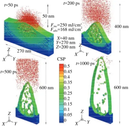
As a result of the presented research, the formation of the final periodic nanostructures on thick Au targets has been investigated both theoretically and experimentally, Fig. 7. In order to simulate the nanostructuring process a hybrid atomistic-continuum (MD-based) super large-scale modeling was applied, which allowed a one-to-one comparison with experiment. The corresponding experimental results were obtained producing an
0.5 0.45 0.4 0.35 0.3 0.25 0.2 0.15 0.1 0.05 0 CSP
Finc=250 mJ/cm2
Fabs=168 mJ/cm
2
50 nm
400 nm
600 nm 600 nm
X=40 nm
Y=270 nm
Z=200 nm
270 nm
t=50 ps t=200 ps
t=500 ps
t=1000 ps
Z Z
Z Z
X
X X
X Y Y
intensity grating on a gold surface with a sinusoidal shape, using single UV-femtosecond laser pulses [19]. The final surface structures were investigated by SEM while the preparation of a TEM cross section allowed a detailed look beneath the surface. The high resolution of the latter technique allowed a direct comparison of the experiment with the results of MD simulation on an atomic scale showing a very good agreement. In Fig. 7, a,
one can see that at the applied fluence of 130 mJ/cm2 the resulting snapshot from the atomic simulation reveals
an empty space beneath the surface, that corresponds to the lighten area (platinum) obtained by FIB technique upon the post experimental treatment of the gold sample. Fig. 7, b, predicts the formation of large number of
monocrystalline structures inside the pre-surface void at the applied fluence of 160 mJ/cm2. And, finally, the
highest applied fluence of 250 mJ/cm2 (Fig. 7, c), leads to a separation of a thin layer, which opens up to the
surface and, simultaneously with the solidification process, forms the closing nanowalls on the sample surface.
a b c
Fig. 7. The obtained in simulations final structures are directly compared [19] with the corresponding experimental SEM images of 270 nm periodic nanostructuring of gold targets with three different average incident fluences
shown in columns for 130 mJ/cm2 (a), 160 mJ/cm2 (b), and 250 mJ/cm2 (c). For the case (a), the obtained structure was treated by Focused Ion Beam (FIB) method to prepare a cross section, shown in Transmission Electron Microscopy (TEM) image for visualization of the internal structures in the center of (a). For the case (b),
the areas of the atomic snapshot in black rectangles are zoomed for better visualization of the obtained internal polycrystalline structures. The red rectangle on the SEM image in (c) shows the relative position of the computational cell when simulating the nanostructuring process. In all atomic snapshots, taken at the final time of
1000 ps, the atoms are colored according the CSP indicating gaseous atoms (red), surface (green), liquid ambient (light blue), dislocation planes and defects (blue), and the atoms with crystalline surrounding (dark blue)
Conclusion
Rapid expansion of the domain of practical applications of ultrashort pulse lasers into new areas where precise nanoscale control of the material modification is required can only be sustained with an improved fundamental understanding of laser-materials interactions. The ability to achieve high spatial resolution with UV laser pulses in material modification and microstructure engineering usually relies on fast and highly localized energy deposition that, unavoidably, creates the conditions of strong electronic, thermodynamic, and mechanical nonequilibrium.
Theoretical and computational description of the materials behavior far from the equilibrium is challenging and requires the revision of existing (or development of new) theoretical models and computational approaches. In particular, the intricate connections between the ultrafast material response to the laser excitation, generation of crystal defects, phase transformations, and mass transfer occurring under highly nonequilibrium conditions can only be accounted for by combining the research expertise and theoretical approaches. Close interdisciplinary collaborations and innovative design of new multiscale approaches (such as MD-TTM model)
0.5 0.45 0.4 0.35 0.3 0.25 0.2 0.15 0.1 0.05 0 CSP 40 nm
130 mJ/cm2 160 mJ/cm2 250 mJ/cm2
5 nm
5 nm
t=800 ps
200 nm
400 nm
Z
Z
Z Z
Y
Y
Y Z
X X
Y X Y
125 mJ/cm2 200 nm 175 mJ/cm2 200 nm 250 mJ/cm2 200 nm
incorporating dissimilar physical concepts and operating at different time- and length-scales are needed for making a significant progress in the theoretical and computational description of laser-material interactions.
The presented work revealed one of the concepts of the internal structures formation on the example of nanocrystalline character of the structures, obtained in the periodic nanostructuring experiments with short UV laser pulses. The applied MD-based model allowed for the direct comparison of the simulated and experimental results and revealed their close match. The demonstrated approach, therefore, opens the way to predict properties of surface modifications for industrial applications. This fact emphasizes that the understanding of these processes on an atomic scale and being able to precisely simulate them provides a powerful tool for designing new nano-technology applications.
Ʌɢɬɟɪɚɬɭɪɚ
1. Chichkov B.N., Momma C., Nolte S., von Alvensleben F., Tünnermann A. Femtosecond, picosecond and nanosecond laser ablation of solids // Applied Physics A. 1996. V. 63. P. 109–115. doi: 10.1007/bf01567637
2. Gattass R.R., Mazur E. Femtosecond laser micromachining in transparent materials // Nature Photonics. 2008. V. 2. P. 219– 225. doi: 10.1038/nphoton.2008.47
3. Vorobyev A.Y., Guo C. Direct femtosecond laser surface nano/microstructuring and its applications // Laser and Photonics Reviews. 2013. V. 7. P. 385–407. doi: 10.1002/lpor.201200017
4. Lin B., Elsayed-Ali H.E. Temperature dependent reflection electron diffraction study of In(1 1 1) and observation of laser-induced transient surface superheating // Surface Science. 2002. V. 498. N 3. P. 275–284. doi: 10.1016/s0039-6028(01)01764-2
5. Siwick B.J., Dwyer J.R., Jordan R.E., Miller R.J.D. An atomic-level view of melting using femtosecond electron diffraction // Science. 2003. V. 302. N 5649. P. 1382–1385. doi: 10.1126/science.1090052
6. Sokolowski-Tinten K., Blome C., Blums J., Cavalleri A., Dietrich C. et. al. Femtosecond X-ray measurement of coherent lattice vibrations near the Lindemann stability limit // Nature. 2003. V. 422. N 6929. P. 287–289. doi: 10.1038/nature01490 7. Ivanov D.S., Zhigilei L.V. Kinetic limit of heterogeneous
melting in metals // Physical Review Letters. 2007. V. 98. N 19. Art. 195701. doi: 10.1103/physrevlett.98.195701
8. Lin Z., Leveugle E., Bringa E.M., Zhigilei L.V. Molecular dynamics simulation of laser melting of nanocrystalline Au // The Journal of Physical Chemistry C. 2010. V. 114. N 12. P. 5686–5699. doi: 10.1021/jp909328q
9. Ivanov D.S., Lin Z., Rethfeld B., O'Connor G.M., Glynn Th.J., Zhigilei L.V. Nanocrystalline structure of nanobump generated by localized photoexcitation of metal film // Journal of Applied Physics. 2010. V. 107. N 1. P. 013519. doi: 10.1063/1.3276161 10. Pronko P.P., Dutta S.K., Squier J., Rudd J.V., Du D., Mourou G. Machining of sub-micron holes using a femtosecond laser at 800nm // Optics Communications. 1995. V. 114. N1-2. P. 106– 110. doi: 10.1016/0030-4018(94)00585-i
11. Koch J., Korte F., Bauer T., Fallnich C., Ostendorf A., Chichkov B.N. Nanotexturing of gold films by femtosecond laser-induced melt dynamics // Applied Physics A. 2005. V. 81. N 2. P. 325–328. doi: 10.1007/s00339-005-3212-6 12. Hwang D., Ryu S.-G., Misra N., Jeon H., Grigoropoulos C.P.
Nanoscale laser processing and diagnostics // Applied Physics A. 2009. V. 96. N 2. P. 289–306. doi: 10.1007/s00339-009-5207-1
13. Huber C., Trügler A., Hohenester U., Prior Y., Kautek W. Optical near-field excitation at commercial scanning probe microscopy tips: a theoretical and experimental investigation // Phys. Chem. Chem. Phys. 2014. V. 16. N 6. P. 2289–2296. doi: 10.1039/c3cp51730f
14. Ivanov D.S., Zhigilei L.V. Combined atomistic-continuum modeling of short-pulse laser melting and disintegration of metal films // Physical Review B. 2003. V. 68. N 6. Art. 064114. doi: 10.1103/physrevb.68.064114
15. .И., . ., . .
// . 1974. . 66. № 2. . 776–781.
16. Leveugle E., Ivanov D.S., Zhigilei L.V. Photochemical spallation of molecular and metal targets: molecular dynamic
References
1. Chichkov B.N., Momma C., Nolte S., von Alvensleben F., Tünnermann A. Femtosecond, picosecond and nanosecond laser ablation of solids. Applied Physics A, 1996, vol. 63, pp. 109–115. doi: 10.1007/bf01567637
2. Gattass R.R., Mazur E. Femtosecond laser micromachining in transparent materials. Nature Photonics, 2008, vol. 2, pp. 219– 225. doi: 10.1038/nphoton.2008.47
3. Vorobyev A.Y., Guo C. Direct femtosecond laser surface nano/microstructuring and its applications. Laser and Photonics Reviews, 2013, vol. 7, pp. 385–407. doi: 10.1002/lpor.201200017
4. Lin B., Elsayed-Ali H.E. Temperature dependent reflection electron diffraction study of In(1 1 1) and observation of laser-induced transient surface superheating. Surface Science, 2002, vol. 498, no. 3, pp. 275–284. doi: 10.1016/s0039-6028(01)01764-2
5. Siwick B.J., Dwyer J.R., Jordan R.E., Miller R.J.D. An atomic-level view of melting using femtosecond electron diffraction. Science, 2003, vol. 302, no. 5649, pp. 1382–1385. doi: 10.1126/science.1090052
6. Sokolowski-Tinten K., Blome C., Blums J., Cavalleri A., Dietrich C. et. al. Femtosecond X-ray measurement of coherent lattice vibrations near the Lindemann stability limit. Nature, 2003, vol. 422, no. 6929, pp. 287–289. doi: 10.1038/nature01490
7. Ivanov D.S., Zhigilei L.V. Kinetic limit of heterogeneous melting in metals. Physical Review Letters, 2007, vol. 98, no. 19, art. 195701. doi: 10.1103/physrevlett.98.195701
8. Lin Z., Leveugle E., Bringa E.M., Zhigilei L.V. Molecular dynamics simulation of laser melting of nanocrystalline Au. The Journal of Physical Chemistry C, 2010, vol. 114, no. 12, pp. 5686–5699. doi: 10.1021/jp909328q
9. Ivanov D.S., Lin Z., Rethfeld B., O'Connor G.M., Glynn Th.J., Zhigilei L.V. Nanocrystalline structure of nanobump generated by localized photoexcitation of metal film. Journal of Applied Physics, 2010, vol. 107, no. 1, pp. 013519. doi: 10.1063/1.3276161
10. Pronko P.P., Dutta S.K., Squier J., Rudd J.V., Du D., Mourou G. Machining of sub-micron holes using a femtosecond laser at 800nm. Optics Communications, 1995, vol. 114, no. 1-2, pp. 106–110. doi: 10.1016/0030-4018(94)00585-i
11. Koch J., Korte F., Bauer T., Fallnich C., Ostendorf A., Chichkov B.N. Nanotexturing of gold films by femtosecond laser-induced melt dynamics. Applied Physics A, 2005, vol. 81, no. 2, pp. 325–328. doi: 10.1007/s00339-005-3212-6
12. Hwang D., Ryu S.-G., Misra N., Jeon H., Grigoropoulos C.P. Nanoscale laser processing and diagnostics. Applied Physics A, 2009, vol. 96, no. 2, pp. 289–306. doi: 10.1007/s00339-009-5207-1
13. Huber C., Trügler A., Hohenester U., Prior Y., Kautek W. Optical near-field excitation at commercial scanning probe microscopy tips: a theoretical and experimental investigation. Phys. Chem. Chem. Phys., 2014, vol. 16, no. 6, pp. 2289–2296. doi: 10.1039/c3cp51730f
14. Ivanov D.S., Zhigilei L.V. Combined atomistic-continuum modeling of short-pulse laser melting and disintegration of metal films. Physical Review B, 2003, vol. 68, no. 6, art. 064114. doi: 10.1103/physrevb.68.064114
study // Applied Physics A. 2004. V. 79. N 1. P. 1643–1655. doi: 10.1007/s00339-004-2682-2
17. Zhigilei L.V., Lin Z., Ivanov D.S. Atomistic modeling of short pulse laser ablation of metals: connections between melting, spallation, and phase explosion // The Journal of Physical Chemistry C. 2009. V. 113. N 27. P. 11892–11906. doi: 10.1021/jp902294m
18. Ivanov D.S., Lipp V.P., Rethfeld B., Garcia M.E. Molecular-dynamics study of the mechanism of short-pulse laser ablation of single-crystal and polycrystalline metallic targets // Journal of Optical Technology. 2014. V. 81. N 5. P. 250–253. doi: 10.1364/jot.81.000250
19. Ivanov D.S., Lipp V.P., Blumenstein A., Veiko V.P., Yakovlev E.B. et. al. Experimental and theoretical investigation of periodic nanostructuring of Au with UV laser near the ablation threshold // Physical Review Applied. 2015. V. 4. N 6. Art. 064006. doi: 10.1103/physrevapplied.4.064006
20. И . ., . ., A., . .,
. ., . ., M.E., .,
И ., .
//
-, . 2015. . 15. № 6. . 984–999.
21. Corkum P.B., Brunel F., Sherman N.K., Srinivasan-Rao T. Thermal response of metals to ultrashort-pulse laser excitation // Physical Review Letters. 1988. V. 61. N 25. P. 2886–2889. doi: 10.1103/physrevlett.61.2886
22. Demsar J., Averitt R.D., Ahn K.H., Graf M.J., Trugman S.A., Kabanov V.V., Sarrao J.L., Taylor A.J. Quasiparticle relaxation dynamics in heavy fermion compounds // Physical Review Letters. 2003. V. 91. N 2. Art. 027401. doi: 10.1103/physrevlett.91.027401
23. Hohlfeld J., Wellershoff S.-S., Güdde J., Conrad U., Jähnke V., Matthias E. Electron and lattice dynamics following optical excitation of metals // Chemical Physics. 2000. V. 251. N 1-3. P. 237–258. doi: 10.1016/s0301-0104(99)00330-4
24. Ihlemann J., Klein-Wiele J.-H., Bekesi J., Simon P. UV ultrafast laser processing using phase masks // Journal of Physics: Conference Series. 2007. V. 59. P. 449–452. doi: 10.1088/1742-6596/59/1/096
25. Bekesi J., Simon P., Ihlemann J. Deterministic sub-micron 2D grating structures on steel by UV-fs-laser interference patterning // Applied Physics A. 2014. V. 114. N 1. P. 69–73. doi: 10.1007/s00339-013-8083-7
26. Borchers B., Bekesi J., Simon P., Ihlemann J. Submicron surface patterning by laser ablation with short UV pulses using a proximity phase mask setup // Journal of Applied Physics. 2010. V. 107. N 6. Art. 063106. doi: 10.1063/1.3331409 27. Eisele C., Nebel C.E., Stutzmann M. Periodic light coupler
gratings in amorphous thin film solar cells // Journal of Applied Physics. 2001. V. 89. N 12. P. 7722–7726. doi: 10.1063/1.1370996
28. Chen J.-T., Lai W.-C., Kao Y.-J, Yang Y.-Y., Sheu J.-J. Laser-induced periodic structures for light extraction efficiency enhancement of GaN-based light emitting diodes // Optics Express. 2012. V. 20. N 5. P. 5689–5695. doi: 10.1364/oe.20.005689
29. Wang C., Chang Y.-C., Yao J., Luo C., Yin S., Ruffin P., Brantley C., Edwards E. Surface enhanced Raman spectroscopy by interfered femtosecond laser created nanostructures // Applied Physics Letters. 2012. V. 100. N 2. Art. 023107. doi: 10.1063/1.3676040
30. Nagy T., Simon P. Single-shot TG FROG for the characterization of ultrashort DUV pulses // Optics Express. 2009. V. 17. N 10. P. 8144–8151. doi: 10.1364/oe.17.008144 31. Ivanov D.S., Rethfeld B., O’Connor G.M., Glynn T.J., Volkov
A.N., Zhigilei L.V. The mechanism of nanobump formation in femtosecond pulse laser nanostructuring of thin metal films // Applied Physics A. 2008. V. 92. N 4. P. 791–796. doi: 10.1007/s00339-008-4712-y
32. Ivanov D.S., Kuznetsov A.I., Lipp V.P., Rethfeld B., Chichkov B.N., Garcia M.E., Schulz W. Short laser pulse nanostructuring of metals: direct comparison of molecular dynamics modeling and experiment // Applied Physics A. 2013. V. 111. N 3. P.
16. Leveugle E., Ivanov D.S., Zhigilei L.V. Photochemical spallation of molecular and metal targets: molecular dynamic study. Applied Physics A, 2004, vol. 79, no. 1, pp. 1643–1655. doi: 10.1007/s00339-004-2682-2
17. Zhigilei L.V., Lin Z., Ivanov D.S. Atomistic modeling of short pulse laser ablation of metals: connections between melting, spallation, and phase explosion. The Journal of Physical Chemistry C, 2009, vol. 113, no. 27, pp. 11892–11906. doi: 10.1021/jp902294m
18. Ivanov D.S., Lipp V.P., Rethfeld B., Garcia M.E. Molecular-dynamics study of the mechanism of short-pulse laser ablation of single-crystal and polycrystalline metallic targets. Journal of Optical Technology, 2014, vol. 81, no. 5, pp. 250–253. doi: 10.1364/jot.81.000250
19. Ivanov D.S., Lipp V.P., Blumenstein A., Veiko V.P., Yakovlev E.B. et. al. Experimental and theoretical investigation of periodic nanostructuring of Au with UV laser near the ablation threshold. Physical Review Applied, 2015, vol. 4, no. 6, art. 064006. doi: 10.1103/physrevapplied.4.064006
20. Ivanov D.S., Lipp V.P., Blumenstein A., Veiko V.P., Yakovlev E.B., Roddatis V.V., Garcia M.E., Rethfeld B., Ihlemann J., Simon P. Analysis of periodic nanostructures formation on a gold surface under exposure to ultrashort laser pulses near the melting threshold. Scientific and Technical Journal of Information Technologies, Mechanics and Optics, 2015, vol. 15, no. 6, pp. 984–999. (in Russian).
21. Corkum P.B., Brunel F., Sherman N.K., Srinivasan-Rao T. Thermal response of metals to ultrashort-pulse laser excitation. Physical Review Letters, 1988, vol. 61, no. 25, pp. 2886–2889. doi: 10.1103/physrevlett.61.2886
22. Demsar J., Averitt R.D., Ahn K.H., Graf M.J., Trugman S.A., Kabanov V.V., Sarrao J.L., Taylor A.J. Quasiparticle relaxation dynamics in heavy fermion compounds. Physical Review Letters, 2003, vol. 91, no. 2, art. 027401. doi: 10.1103/physrevlett.91.027401
23. Hohlfeld J., Wellershoff S.-S., Güdde J., Conrad U., Jähnke V., Matthias E. Electron and lattice dynamics following optical excitation of metals. Chemical Physics, 2000, vol. 251, no. 1-3, pp. 237–258. doi: 10.1016/s0301-0104(99)00330-4
24. Ihlemann J., Klein-Wiele J.-H., Bekesi J., Simon P. UV ultrafast laser processing using phase masks. Journal of Physics: Conference Series, 2007, vol. 59, pp. 449–452. doi: 10.1088/1742-6596/59/1/096
25. Bekesi J., Simon P., Ihlemann J. Deterministic sub-micron 2D grating structures on steel by UV-fs-laser interference patterning. Applied Physics A. 2014, vol. 114, no. 1, pp. 69–73. doi: 10.1007/s00339-013-8083-7
26. Borchers B., Bekesi J., Simon P., Ihlemann J. Submicron surface patterning by laser ablation with short UV pulses using a proximity phase mask setup. Journal of Applied Physics, 2010, vol. 107, no. 6, art. 063106. doi: 10.1063/1.3331409 27. Eisele C., Nebel C.E., Stutzmann M. Periodic light coupler
gratings in amorphous thin film solar cells. Journal of Applied Physics, 2001, vol. 89, no. 12, pp. 7722–7726. doi: 10.1063/1.1370996
28. Chen J.-T., Lai W.-C., Kao Y.-J, Yang Y.-Y., Sheu J.-J. Laser-induced periodic structures for light extraction efficiency enhancement of GaN-based light emitting diodes. Optics Express, 2012, vol. 20, no. 5, pp. 5689–5695. doi: 10.1364/oe.20.005689
29. Wang C., Chang Y.-C., Yao J., Luo C., Yin S., Ruffin P., Brantley C., Edwards E. Surface enhanced Raman spectroscopy by interfered femtosecond laser created nanostructures. Applied Physics Letters, 2012, vol. 100, no. 2, art. 023107. doi: 10.1063/1.3676040
30. Nagy T., Simon P. Single-shot TG FROG for the characterization of ultrashort DUV pulses. Optics Express, 2009, vol. 17, no. 10, pp. 8144–8151. doi: 10.1364/oe.17.008144
31. Ivanov D.S., Rethfeld B., O’Connor G.M., Glynn T.J., Volkov A.N., Zhigilei L.V. The mechanism of nanobump formation in femtosecond pulse laser nanostructuring of thin metal films. Applied Physics A, 2008, vol. 92, no. 4, pp. 791–796. doi: 10.1007/s00339-008-4712-y
675–687. doi: 10.1007/s00339-013-7656-9
33. Schäfer C., Urbassek H.M., Zhigilei L.V., Garrison B.J. Pressure-transmitting boundary conditions for molecular dynamics simulations // Computational Materials Science. 2002. V. 24. N 4. P. 421–429. doi: 10.1016/s0927-0256(01)00263-4
34. Zhakhovskii V.V., Inogamov N.A., Petrov Yu.V., Ashitkov S.I., Nishihara K. Molecular dynamics simulation of femtosecond ablation and spallation with different interatomic potentials // Applied Surface Science. 2009. V. 255. N 24. P. 9592–9596. doi: 10.1016/j.apsusc.2009.04.082
35. Smithell’s Metal Reference Book. 8th ed. / Eds. W.F. Gale, T.C.
Totemeier. Butterworth-Heinemann, Oxford, 2004. 2080 p. 36. Ivanov D.S., Lipp V.P., Veiko V.P., Yakovlev E., Rethfeld B.,
Garcia M.E. Molecular dynamics study of the short laser pulse ablation: quality and efficiency in production // Applied Physics A. 2014. V. 117. N 4. P. 2133–2141. doi: 10.1007/s00339-014-8633-7
37. Wu B., Shin Y.C. A self-closed thermal model for laser shock peening under the water confinement regime configuration and comparisons to experiments // Journal of Applied Physics. 2005. V. 97. N 11. Art. 113517. doi: 10.1063/1.1915537 38. Nakano H., Miyauti S., Butani N., Shibayanagi T., Tsukamoto
M., Abe N. Femtosecond laser peening of stainless steel // Journal of Laser Micro/Nanoengineering. 2009. V. 4. N 1. P. 35–38. doi: 10.2961/jlmn.2009.01.0007
39. Nakano H., Tsuyama M., Miyauti S., Shibayanagi T., Tsukamoto M., Abe N. Femtosecond and nanosecond laser peening of stainless steel // Journal of Laser Micro/Nanoengineering. 2010. V. 5. N 2. P. 175–178. doi: 10.2961/jlmn.2009.01.0007
40. Cheng G.J., Shehadeh M.A. Dislocation behavior in silicon crystal induced by laser shock peening: a multiscale simulation approach // Scripta Materialia. 2005. V. 53. N 9. P. 1013–1018. doi: 10.1016/j.scriptamat.2005.07.014
41. Wu C., Zhigilei L.V. Nanocrystalline and polyicosahedral structure of a nanospike generated on metal surface irradiated by a single femtosecond laser pulse // Journal of Physical Chemistry C. 2016. V. 120. N 8. P. 4438–4447. doi: 10.1021/acs.jpcc.6b00013
42. Valiev R.Z., Islamgaliev R.K., Alexandrov I.V. Bulk nanostructured materials from severe plastic deformation // Progress in Materials Science. 2000. V. 45. N 2. P. 103–189. doi: 10.1016/s0079-6425(99)00007-9
43. Bufford D.C., Morris Wang Y., Liu Y., Li L. Synthesis and microstructure of electrodeposited and sputtered nanotwinned face-centered-cubic metals // MRS Bulletin. 2016. V. 41. N 4. P. 286–291. doi: 10.1557/mrs.2016.62
44. Fang T.H., Li W.L., Tao N.R., Lu K. Revealing extraordinary intrinsic tensile plasticity in gradient nano-grained copper // Science. 2011. V. 331. N 6024. P. 1587–1590. doi: 10.1126/science.1200177
45. Jang D., Li X., Gao H., Greer J.R. Deformation mechanisms in nanotwinned metal nanopillars // Nature Nanotechnology. 2012. V. 7. N 9. P. 594–601. doi: 10.1038/nnano.2012.116 46. Li X., Dao M., Eberl C., Hodge A.M., Gao H. Fracture,
fatigue, and creep of nanotwinned metals // MRS Bulletin. 2016. V. 41. N 4. P. 298–304. doi: 10.1557/mrs.2016.65 47. Ivanov D.S., Rethfeld B.C. The effect of pulse duration on the
interplay of electron heat conduction and electron–phonon interaction: photo-mechanical versus photo-thermal damage of metal targets // Applied Surface Science. 2009. V. 255. N 24. P. 9724–9728. doi: 10.1016/j.apsusc.2009.04.131
48. И . ., . ., .И.,
. ., . ., .И., ., . .
// . 2008. . 134. № 1. . 1–29. 49. Upadhyay A.K., Inogamov N.A., Rethfeld B., Urbassek H.M.
Ablation by ultrashort laser pulses: atomistic and thermodynamic analysis of the processes at the ablation threshold // Physical Review B. 2008. V. 78. N 4. Art. 045437. doi: 10.1103/physrevb.78.045437
50. Wellershoff S.-S., Hohlfeld J., Güdde J., Matthias E. The role of electron–phonon coupling in femtosecond laser damage of metals // Applied Physics A. 1999. V. 69. P. S99–S107. doi: 10.1007/s003399900305
of metals: direct comparison of molecular dynamics modeling and experiment. Applied Physics A, 2013, vol. 111, no. 3, pp. 675–687. doi: 10.1007/s00339-013-7656-9
33. Schäfer C., Urbassek H.M., Zhigilei L.V., Garrison B.J. Pressure-transmitting boundary conditions for molecular dynamics simulations. Computational Materials Science, 2002, vol. 24, no. 4, pp. 421–429. doi: 10.1016/s0927-0256(01)00263-4
34. Zhakhovskii V.V., Inogamov N.A., Petrov Yu.V., Ashitkov S.I., Nishihara K. Molecular dynamics simulation of femtosecond ablation and spallation with different interatomic potentials. Applied Surface Science, 2009, vol. 255, no. 24, pp. 9592–9596. doi: 10.1016/j.apsusc.2009.04.082
35. Smithell’s Metal Reference Book. 8th ed. Eds. W.F. Gale, T.C.
Totemeier. Butterworth-Heinemann, Oxford, 2004, 2080 p. 36. Ivanov D.S., Lipp V.P., Veiko V.P., Yakovlev E., Rethfeld B.,
Garcia M.E. Molecular dynamics study of the short laser pulse ablation: quality and efficiency in production. Applied Physics A, 2014, vol. 117, no. 4, pp. 2133–2141. doi: 10.1007/s00339-014-8633-7
37. Wu B., Shin Y.C. A self-closed thermal model for laser shock peening under the water confinement regime configuration and comparisons to experiments. Journal of Applied Physics, 2005, vol. 97, no. 11, art. 113517. doi: 10.1063/1.1915537
38. Nakano H., Miyauti S., Butani N., Shibayanagi T., Tsukamoto M., Abe N. Femtosecond laser peening of stainless steel. Journal of Laser Micro/Nanoengineering, 2009, vol. 4, no. 1, pp. 35–38. doi: 10.2961/jlmn.2009.01.0007
39. Nakano H., Tsuyama M., Miyauti S., Shibayanagi T., Tsukamoto M., Abe N. Femtosecond and nanosecond laser peening of stainless steel. Journal of Laser Micro/Nanoengineering, 2010, vol. 5, no. 2, pp. 175–178. doi: 10.2961/jlmn.2009.01.0007
40. Cheng G.J., Shehadeh M.A. Dislocation behavior in silicon crystal induced by laser shock peening: a multiscale simulation approach. Scripta Materialia, 2005, vol. 53, no. 9, pp. 1013– 1018. doi: 10.1016/j.scriptamat.2005.07.014
41. Wu C., Zhigilei L.V. Nanocrystalline and polyicosahedral structure of a nanospike generated on metal surface irradiated by a single femtosecond laser pulse. Journal of Physical Chemistry C, 2016, vol. 120, no. 8, pp. 4438–4447. doi: 10.1021/acs.jpcc.6b00013
42. Valiev R.Z., Islamgaliev R.K., Alexandrov I.V. Bulk nanostructured materials from severe plastic deformation. Progress in Materials Science, 2000, vol. 45, no. 2, pp. 103– 189. doi: 10.1016/s0079-6425(99)00007-9
43. Bufford D.C., Morris Wang Y., Liu Y., Li L. Synthesis and microstructure of electrodeposited and sputtered nanotwinned face-centered-cubic metals. MRS Bulletin, 2016, vol. 41, no. 4, pp. 286–291. doi: 10.1557/mrs.2016.62
44. Fang T.H., Li W.L., Tao N.R., Lu K. Revealing extraordinary intrinsic tensile plasticity in gradient nano-grained copper. Science, 2011, vol. 331, no. 6024, pp. 1587–1590. doi: 10.1126/science.1200177
45. Jang D., Li X., Gao H., Greer J.R. Deformation mechanisms in nanotwinned metal nanopillars. Nature Nanotechnology, 2012, vol. 7, no. 9, pp. 594–601. doi: 10.1038/nnano.2012.116 46. Li X., Dao M., Eberl C., Hodge A.M., Gao H. Fracture,
fatigue, and creep of nanotwinned metals. MRS Bulletin, 2016, vol. 41, no. 4, pp. 298–304. doi: 10.1557/mrs.2016.65 47. Ivanov D.S., Rethfeld B.C. The effect of pulse duration on the
interplay of electron heat conduction and electron–phonon interaction: photo-mechanical versus photo-thermal damage of metal targets. Applied Surface Science, 2009, vol. 255, no. 24, pp. 9724–9728. doi: 10.1016/j.apsusc.2009.04.131
48. Inogamov N.A., Zhakhovskii V.V., Ashitkov S.I., Petrov Yu.V., Agranat M.B., Anisimov S.I., Nishihara K., Fortov V.E. Nanospallation induced by an ultrashort laser pulse. Journal of Experimental and Theoretical Physics, 2008, vol. 107, no. 1, pp. 1–19. doi: 10.1134/s1063776108070017
49. Upadhyay A.K., Inogamov N.A., Rethfeld B., Urbassek H.M. Ablation by ultrashort laser pulses: atomistic and thermodynamic analysis of the processes at the ablation threshold. Physical Review B, 2008, vol. 78, no. 4, art. 045437. doi: 10.1103/physrevb.78.045437
51. Veiko V.P., Shakhno . ., Yakovlev E.B. Effective time of thermal effect of ultrashort laser pulses on dielectrics // Quantum Electronics. 2014. V. 44. N 4. P. 322–324. doi: 10.1070/qe2014v044n04abeh015324
52. Wu C., Zhigilei L.V. Microscopic mechanisms of laser spallation and ablation of metal targets from large-scale molecular dynamics simulations // Applied Physics A. 2014. V. 114. N 1. P. 11–32. doi: 10.1007/s00339-013-8086-4
of electron–phonon coupling in femtosecond laser damage of metals. Applied Physics A, 1999, vol. 69, pp. S99–S107. doi: 10.1007/s003399900305
51. Veiko V.P., Shakhno . ., Yakovlev E.B. Effective time of thermal effect of ultrashort laser pulses on dielectrics. Quantum Electronics, 2014, vol. 44, no. 4, pp. 322–324. doi: 10.1070/qe2014v044n04abeh015324
52. Wu C., Zhigilei L.V. Microscopic mechanisms of laser spallation and ablation of metal targets from large-scale molecular dynamics simulations. Applied Physics A, 2014, vol. 114, no. 1, pp. 11–32. doi: 10.1007/s00339-013-8086-4
Ⱥɜɬɨɪɵ Authors
И –
-, , ,
, 34132, ; ,
, ,
67663, ;
, И , - , 197101,
Dmitry S. Ivanov – PhD, Senior research scientist, University of Kassel, Kassel, 34132, Germany; Senior research scientist, Technical University of Kaiserslautern, Kaiserslautern, 67663, Germany; Director of International laboratory, ITMO University, Saint Petersburg, 197101, Russian Federation, [email protected]
– ,
ё , ё , 37077, ; ,
, , 34132, , [email protected]
Andreas Blumesntein – postgraduate, Laser-Laboratorium-Göttingen e.V., Laser-Laboratorium-Göttingen, 37077, Germany; postgraduate, University of Kassel, Kassel, 34132, Germany, [email protected]
ф ь ь – , ,
,
, , 67663, ,
Barbel Rethfeld – D.Sc., Professor, Head of Ultrafast Dynamics of Laser Excited Solids group, University of Kaiserslautern, Kaiserslautern, 67663, Germany, [email protected]
– , ,
, И , - ,
197101, , [email protected]
Vadim P. Veiko – D.Sc., Professor, Head of Chair, ITMO University, Saint Petersburg, 197101, Russian Federation, [email protected]
– , ,
, И , - , 197101,
Evgeny B. Yakovlev –D.Sc., Associate professor, Professor, ITMO University, Saint Petersburg, 197101, Russian Federation, [email protected]
М Э ь – PhD, , ,
, , 34132, ,
Martin E. Garcia–PhD, Full Professor, University of Kassel, Kassel, 34132, Germany, [email protected]
Ⱦɦɢɬɪɢɣ ɋɟɪɝɟɟɜɢ ɂɜɚɧɨɜ 1997 .
--
« ». 2004 . PhD
( ).
. .
. 2015 . – «
-- » ,
( И ) . - .
-, ,
-, .
Dmitry S. Ivanov graduated from Physico-Technical Department of Peter the Great St. Petersburg Politechnic University (Politech) in 1997 with specialization of "Space Research". In 2004 he obtained his PhD degree in the University of Virginia (USA). At present he works as a Senior Researcher at Technical University of Kaiserslautern and University of Kassel (Germany). Also, since 2015 he has been a co-chief of the International Laboratory of “Laser Micro- and Nanotechnologies” at Saint Petersburg State University of Information Technologies, Mechanics and Optics (Russia). His scientific research interests cover modeling of short laser pulse melting, spallation, ablation processes as well as laser-induced nanostructuring of metals, semiconductors, and dielectric surfaces.
ȺɧɞɪɟɚɫȻɥɸɦɟɧɲɬɚɣɧ ё
2013 . .
– ё
( ).
.
ȻɚɪɛɟɥɶɊɟɬɮɟɥɶɞ – . 2013 . – . . 1999 .
PhD . .
. ( ),
. . . ( ,
).
.
-. .
DFG ( ). –
.
Barbel Rethfeld is a Heisenberg Professor of Applied Theoretical Physics at the University of Kaiserslautern since 2013. She received her PhD degree from the University of Braunschweig in 1999 and has worked since then at the University of Essen, Germany, L.D. Landau Institute for Theoretical Physics in Moscow, Russia, and GSI Helmholtz Institute in Darmstadt, Germany.In 2007 she established her own research group at the University of Kaiserslautern, after she was awarded an Emmy Noether grant from the German Research Foundation (DFG). Her research interest is in the theoretical description of ultrafast dynamics of laser-excited solids with an emphasis on nonequilibrium processes.
ȼɚɞɢɦɉɚɜɥɨɜɢɱȼɟɣɤɨ – , ,
,
, (1986)
(2010).
« -
-». –
-, . 300 ,
12 , .
Vadim P. Veiko – D.Sc., Professor, Head of Laser Technologies and Systems Department of Saint Petersburg State University of Information Technologies, Mechanics, and Optics (ITMO University). He is an Honored scientist of the Russian Federation, USSR State Prize winner in the field of science (1986), RF Government Prize winner in the field of education (2010). He is a Head of the International Laboratory of “Laser Micro- and Nanotechnologies”. His scientific research interests cover such fields like Laser-Mutter Interaction, Fundamentals of Laser Technologies, etc. He is the author and coauthor of more than 300 scientific publications, among them 12 monographs in Russian, English and Chinese.
ȿɜɝɟɧɢɣ Ȼɨɪɢɫɨɜɢɱ əɤɨɜɥɟɜ – ,
И ( . - ).
. 1985 .
« ,
», 1999 . – «
- ».
«
(1976 .), (1983 .),
«
» (2010 .).
«Fundamentals of Laser Assisted Micro– and
Nanotechnologies» (FLAMN). –
, . 160
, . «И .
-», .
Ɇɚɪɬɢɧȿ. Ƚɚɪɫɢɹ – . ,
. ( , ) 1984 .
« » 1992 . (PhD)
.
(PostDoc) И
, 1999 .
-.
. ( ) И .
2004 .
. ( ). 2006 2008 .
.
-, ,
-, ,
.

![Fig. 7. The obtained in simulations final structures are directly compared [19] with the corresponding experimental SEM images of 270 nm periodic nanostructuring of gold targets with three different average incident fluences](https://thumb-eu.123doks.com/thumbv2/123dok_br/18132504.325487/9.892.132.766.290.747/simulations-structures-directly-compared-corresponding-experimental-nanostructuring-different.webp)
