*e-mail: [email protected]
Effects of Annealing on Electrical and Optical Properties
of a Multilayer InAs/GaAs Quantum Dots System
Adenilson José Chiquitoa*, Yuri Alexander Pusepb, Sérgio Mergulhãoa, Yara Galvão Gobatoa, José Cláudio Galzerania, Nicolai Moshegovc
aDepartamento de Física, Universidade Federal de São Carlos,
CP 676, 13565-905 São Carlos - SP, Brazil
bInstituto de Física de São Carlos, Universidade de São Paulo,
13650-970 São Carlos - SP, Brazil
cThe Pennsylvania State University, Pennsylvania,16802
Received: December 8, 2003; Revised: March 21, 2004
A systematic investigation of the properties of the InAs/GaAs self-assembled quantum dots (SAQDs) system subjected to a post-growth annealing using capacitance-voltage, Raman scatter-ing and photoluminescence measurements is presented. The application of both electrical and optical methods allowed us to obtain reliable information on the microscopic structural evolution of this system. The single layer and the multilayer quantum dots were found to respond differently to the annealing process, due to the differences in strain that occur in both systems. The diffusion activated by strain provoked the appearance of an InGaAs alloy layer in substitution to the quan-tum dots layers; this change occurred at the annealing temperature T = 600 °C in the multilayer system. A single dot layer, however, was observed even after the annealing at T = 700 °C. Moreo-ver, the low temperature annealing was found to improve the homogeneity of the multilayer sys-tem and to decrease the electrical interlayer coupling.
Keywords: InAs/GaAs quantum dots, capacitance, raman scattering
1. Introduction
In recent years, self-assembled quantum dots (SAQDs) have attracted much attention due to their peculiar electronic and optical properties interesting both to fundamental phys-ics and technological applications. The formation of the dots is usually based on the transformation of a strained layer into an assembly of islands of atoms when the two dimen-sional growth changes into a three dimendimen-sional one. This is
the so-called Stranski-Krastanow growth mode1.
The strong quantum confinement of the carriers pre-sented by these defect-free quantum dots makes them an important structure for the development of electronic de-vices. However, the fabrication of reproducible homogene-ous SAQDs structures suitable for applications remains to be achieved. Usually, in order to control the homogeneity of the dots, both the deposition rate and the substrate tem-perature are varied during the growth process. On the other hand, the structure of the SAQDs can be made uniform by a post-growth annealing. As a matter of fact, the influence of
the annealing was reported using the combination of pho-toluminescence (PL) and transmission electron
microscopy2-6. Homogeneous samples were shown to
local electrical behavior. Meanwhile, the phonon Raman scattering is a widely recognized structural sensitive tool. As we shall see, a relatively low annealing temperature (500 °C) improved the homogeneity of the electron distri-bution and caused the decrease of the electrical coupling between the planes containing the dots. The Raman scatter-ing, sensitive to structural modifications, provided evidences of a reorganization of the SAQDs system (SAQDs + barri-ers). However, in contrast to the data presented in Refs. 3,4 where the dots were found to survive even after the anneal-ing at rather high temperatures (700-900 °C) in multilayer SAQDs structures, we observed their disappearance already at 600 °C. A much higher temperature resistance to the an-nealing temperature was indeed observed in a single layer structure. We suppose that the thermal stability of the SAQDs structure strongly depends on the growth conditions result-ing in different strain distributions over the InAs/GaAs struc-ture.
2. Experiment
The samples were grown by a MECA 2000 molecular-beam epitaxy system on (100) GaAs highly doped substrates; they were based on planes containing the InAs SAQDs embedded in a field effect device. The five InAs layers with nominal thicknesses 2.3 monolayers (ML) sepa-rated by 15 ML’s of GaAs were grown at 450 °C. The proc-ess of the dots formation was monitored by reflection of high-energy electron diffraction (RHEED): the transition from a streaked to a spotty RHEED pattern, indicating the formation of 3D islands, was observed after the deposition of 1.8 ML thick InAs. After the growth of SAQDs, an undoped GaAs separating layer (25 nm) was grown, fol-lowed by an undoped GaAs/AlAs (1 nm/3 nm) superlattice in order to increase the electrical impedance of the sam-ples. Finally, the structure was capped with a 5 nm GaAs layer in order to prevent the surface oxidation. During the growth, the InAs and GaAs fluxes were fixed at 0.1 and 0.35 ML/s respectively, while PAs = 5 × 10⁻⁶ Pa. The used samples (labeled A and B) are distinguished by different Si doping levels of the GaAs regions where the dots were
grown: = 5 × 1017 cm-3 and = 1 × 1017 cm-3. The post-growth annealing process was done in an ar-gon atmosphere at different temperatures during 20 min. A control sample with only a single InAs plane was grown in a similar way to those described above.
For the Schottky diode construction, we fabricated a conventional ohmic contact to the substrate with an AuGeNi alloy annealed at 450 °C for 120 s; the Schottky contact was formed by the deposition of a 200 nm gold layer with
500 µm diameter. The capacitance was measured using
standard lock-in techniques (with a SR530 Stanford dual-phase lock-in amplifier). The samples were mounted in a
variable temperature cryostat (Janis CCS350) and the C-V curves were obtained at 10 K.
Unpolarized back-scattering Raman spectra were per-formed at 10 K with a Jobin Yvon T64000 triple spectrometer supplied with a charge coupled device (CCD) detector cooled by liquid nitrogen; PL measurements were also performed at 10 K with a Spex 500M single spectrometer using a photomultiplier tube. The 514.5 nm and 457.9 nm lines of an Ar+ laser were used for excitation (Raman and PL, respectively). In order to measure Raman and PL spectra, the top layers containing the GaAs/AlAs superlattice were first removed.
3. Results and Discussion
In order to deal with the C-V measurements, the spatial distribution of the electrons along the growth direction was calculated by the usual equations for the C-V profile7,
(1)
and
(2)
where C is the measured capacitance, S is the Schottky device area and the other symbols have their usual meanings.
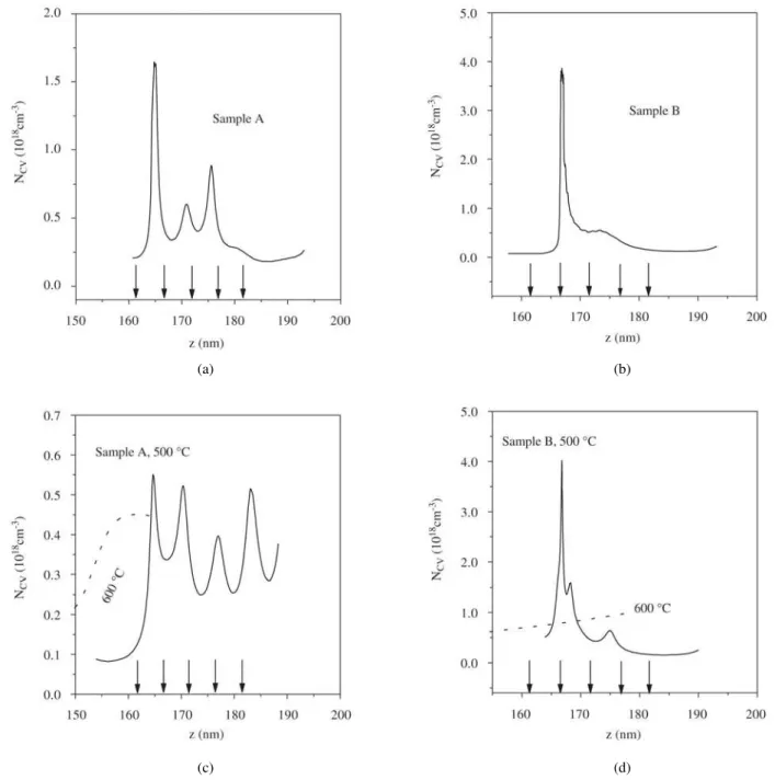
dot-Figure 1. C-V profiles of the as-grown multilayer samples A and B are showed in panels a) and b). Panels c) and d) show the correspond-ing C-V profiles after the annealcorrespond-ing processes. Note that in the sample A (panel c)) the peaks have comparable intensities after the annealing. The dotted lines in panels c) and d) correspond to the annealing at 600°C. Panel e) shows the C-V profiles of the control sample at different annealing temperatures and panel f) shows the C-V profiles calculated for different doping levels in the GaAs barriers: ND = 1020 cm-3 (full line) and N
D = 10
19 cm-3 (dashed line). (Continues on next page)
(a) (b)
(c) (d)
ted lines in Figs. 1c and 1d. This is a first indication that the dots disappeared after the second annealing process (600 °C) in these multilayer samples.
Due to the small separation between the InAs layers, the dots located in adjacent planes were vertically correlated
during the growth9 and electronically coupled, which is
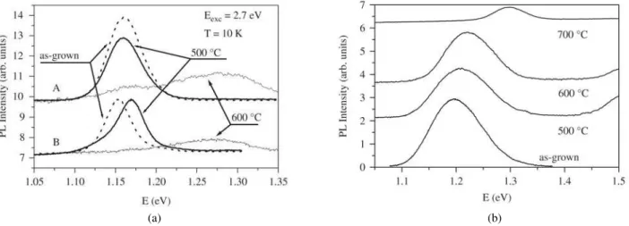
and on the dopant concentration10: with the increase of the doping level the InAs dots planes become more electrically isolated thus showing the effect of screening (Figs. 1a,1b). The corresponding PL spectra of the samples are de-picted in Fig. 2a. They show no significant influence of the low temperature annealing at 500 °C (full lines) in com-parison with the as-grown results (dotted lines). Although the low temperature annealing did not yet influence the prop-erties of the whole multilayer SAQDs system (measured by PL), it significantly modified the individual properties of the layers (measured by C-V). This was clearly indicated by the increase of the electron localization inside the planes containing the dots (C-V profiles observed after the anneal-ing of 500 °C). The samples annealed at a higher tempera-ture (600 °C) revealed a strong modification of the PL spec-tra: the intensities of the lines associated with the SAQDs drastically decreased and a new blue shifted broad line ap-peared around 1.3 eV.
The homogenization of the SAQDs and the increase in the localization of electrons observed by the C-V measure-ments suggest possible structural alterations of the dots2-6. Using Raman scattering, sensitive to local structural modifications, we were able to confirm the reorganization of the SAQDs systems. The Raman spectra of samples with different doping levels, measured before and after the an-nealing process in the frequency range of the InAs optical phonons are shown in Fig. 3a. In both samples the TO mode
was detected. The phonon lines are shifted due to the strain. In the configuration of back-scattering from the (001) sur-face we expect the singlet LO mode and the doublet TO mode to appear in the Raman spectra. The analysis of the
strain field in the SAQDs11,12 shows that both the modes
should present a blue shift. In Ref. 13 we have already found
the TO and LO phonons in InAs/GaAs SAQDs at 250 cm-1
and 260 cm-1, respectively. Therefore, we here assign the
line observed at 250 cm-1 to the TO phonon of InAs, while
no contribution was found at the frequencies where the LO phonons of InAs were expected. The weak line found at
212 cm-1 is probably due to the disorder activated LA
(DALA) phonon of GaAs. We did not find any significant shift of the bulk-like InAs phonon frequencies after the low temperature annealing process, which evidenced that the bulk structure of the SAQDs was not yet changed.
The Raman spectra measured in the frequency range of the GaAs optical phonons are presented in Fig. 3b. In this case both the LO and TO bulk phonons were clearly de-tected. In the as-grown samples they reveal red shifted fre-quencies due to the strain in the GaAs barriers.
In addition, a strong contribution of the GaAs-like opti-cal phonons with large wave vectors reflecting the one-phonon density of states was detected between the TO and LO lines. This defect induced Raman scattering decreased drastically in the samples annealed at T = 600 °C (Fig. 3b). It seems that the multilayer SAQDs structures caused a strong
Figure 1. C-V profiles of the as-grown multilayer samples A and B are showed in panels a) and b). Panels c) and d) show the correspond-ing C-V profiles after the annealcorrespond-ing processes. Note that in the sample A (panel c)) the peaks have comparable intensities after the annealing. The dotted lines in panels c) and d) correspond to the annealing at 600°C. Panel e) shows the C-V profiles of the control sample at different annealing temperatures and panel f) shows the C-V profiles calculated for different doping levels in the GaAs barriers: ND = 1020 cm-3 (full line) and N
D = 10
19 cm-3 (dashed line).
violation of the Raman selection rules, while after the higher temperature annealing relatively homogeneous alloy layers were formed. Mostly the zone-center phonons of GaAs con-tributed to Raman scattering of the studied structures.
The observed modifications of the Raman spectra are explained as following: in the as-grown samples the defect induced Raman scattering of the optical phonons with large wave vectors dominate in the GaAs barriers, while the lines
due to the bulk-like GaAs phonons (both TO and LO) re-veal red shifted frequencies due to the strain. After the an-nealing at 600 °C the SAQDs disappeared and instead,
ho-mogeneous InxGa1-xAs alloy layers were formed. As a
re-sult, the defect induced GaAs-like modes (DALA and the modes with large wave vectors) were eliminated. The shoul-ders found at the low frequency sides of the LO Raman lines correspond to the GaAs-like phonons of the
Figure 3. Raman spectra of the both multilayer and control samples. Panel a) shows the Raman spectra measured before and after the annealing process in the frequency range of the InAs optical phonons. The Raman spectra measured in the frequency range of the GaAs optical phonons are presented in panel (b). Full and dotted lines represent the annealed at 500 °C and as-grown samples, respectively. The thin lines were obtained after the annealing at 600 °C. At the bottom of the figures the Raman spectra of both the as-grown and annealed (700 °C) control sample are presented.
Figure 2. Panel a) shows the PL spectra of the as-grown multilayer samples A and B (dotted lines) taken at 10 K. The corresponding spectra after the annealing at 500 °C are shown by full lines. The thin lines were obtained after the annealing at 600 °C. Panel b) shows the PL spectra of the control sample with a single plane containing dots after the annealing at different temperatures. The curves were shifted up for clearness.
(a) (b)
In0.08Ga0.92As alloy. We did not detect any evidences of the InAs-like phonons in the alloy.
As it was mentioned above, the PL spectra of the struc-tures annealed at 600 °C show a strong blue shift and a broadening of the PL lines with significant decrease of their intensities (Fig. 2a). These shifted PL lines can be attrib-uted to an InxGa1-xAs alloy with × ≈ 0.10 formed as a result of the annealing. This amount of In of the alloy agrees with the value found by Raman scattering. It is worth mention-ing that the formation of the plasmon-LO phonon coupled modes is expected in the doped InAs/GaAs SAQDs struc-tures subjected to the high temperature annealing due to the elimination of the localization potential of the SAQDs. This was not observed in our experiments probably due to the strong localization of the electrons in the InGaAs alloy now caused by defects.
Thus, we can conclude that the annealing at a tempera-ture close to the growth temperatempera-ture slightly improved the localization properties of the InAs/GaAs SAQDs system probably due to the increase of the concentration of free electrons (resulting in the decrease of the screening length) caused by the annealing of the point defects located in the GaAs barriers.
The annealing at 600 °C induced a diffusion process
eliminating the SAQDs and forming an InxGa1-xAs alloy
layer. A similar low-temperature diffusion process induc-ing a post-growth structural modification of the SAQDs was also detected in Ref. 5. We suppose that such low tempera-ture diffusion was stimulated by the interlayer strain. In or-der to confirm this supposition we studied the effect of the annealing process in the single-layer SAQDs system (the control sample) and the results are depicted in Fig. 1e.
Additionally, we performed a simple qualitative simu-lation of the C-V characteristics of the multilayered struc-tures using the Poisson’s equation with the electron density described by the Boltzmann’s statistics. The results indeed show that an increase in the electron concentration in the barriers causes a reasonable improvement of the calculated C-V profile (Fig. 1f) as it was obtained from the experi-mental measurements.
Figure 2b shows the PL spectra of this sample after annealings at different temperatures. Contrary to the results obtained in the multilayer samples, even after the annealings at 600 °C and 700 °C we still observed the PL lines due the SAQDs, which were slightly blue shifted and broadened with the increase of the annealing temperature. Similar modifications of the PL lines were found in the annealed SAQDs in Refs. 2 - 4,6. The C-V data also revealed a ther-mal stability of the single-layer SADQs sample. Following our previous work14, the dispersion of the electron energy
in the SAQDs (∆ ε) were calculated from the C-V
measure-ments. Both the calculated dispersion energies and the spec-tral widths of the PL lines decreased as the annealing
tem-perature increased.
The Raman spectra of the single layer SAQDs sample shown in Figs. 3a and 3b revealed the presences of the InAs optical phonons and the GaAs-like defect induced modes associated with the dots even after the annealing at 700 °C. Thus, the low temperature annealing (at the temperature somewhat higher than the growth temperature) results in a drastic modification of the multilayer SAQDs, while the single layer structure revealed a thermal stability even at rather high temperatures (until 700 °C). These data confirm the role of the interlayer strain in the low temperature diffu-sion process.
4. Conclusion
In summary, we believe that the results presented in this paper constitute direct evidence that a post-growth anneal-ing process can change the electronic properties of the multilayer SAQDs system. After a low temperature anneal-ing, the individual contributions of each plane containing the dots were clearly seen. This implies in a decrease of the carrier coupling between the dots caused by the correspond-ing increase of the strength of the electron localization. In addition, we observed that after the annealing at 600 °C the InAs dots are diluted and the multilayer system produced an InxGa1-xAs alloy layer (× ≈ 0.10), while the single dot
layer system revealed the presence of quantum dots even after the annealing at 600 °C.
The authors would like to acknowledge E. Diagonel for the technical assistance. This work was partially supported by the Brazilian agencies, CNPq and FAPESP.
References
1. Goldstein,L.; Glas, F.; Marzin, J.Y.; Charasse, M.N.;
LeRoux, G. Appl. Phys. Lett. 47, 1099, 1985.
2. Leon, R.; Kin, Y.; Jagadish, C.; Gal, M.; Zou, J. Cockayne, D.H. J. Appl. Phys. Lett. 69, 1888, 1996. 3. Ko sogov, A.O.; Werner, P.; Gösele, U.; Bimberg, N.;
Ustinov, V.M.; Egorov, A.Y.; Zhuokov, A.E.; Kop’ev, P.S.; Bert, N.A.; Alferov, Z.I. Appl. Phys. Lett. 69, 3072, 1996.
4. Malik, S.; Roberts, C.; Murray, R. Pate, M. Appl. Phys.
Lett. 71, 1987, 1997.
5. Johansson, J.; Seifert, W.; Zwiller, V.; Junno, T. Samuelson, L. Appl. Surf. Sci. v. 134, p. 47, 1998. 6. Fafard, S.; Wasilewski, Z.R.; Allen, C.Ni.; Picard, D.;
Spaner, M.; McCaffrey, J.P.; Piva, P.G. Phys. Rev. B
59,15368, 1999.
7. Rhoderick, E.H.; Williams, R.H. Metal-semiconductor
Contacts (Oxford, Cambridge) 1988.
8. Grundmann, M.; Christen, J.; Ledentsov, N.N.; Böhrer, J.; Bimberg, D.; Ruvimov, S.S.; Werner, P.; Richter, U.; Gösele, U.; Heydenreich, J.; Ustinov, V.M.; Egorov,
Rev. Lett. 74, 4043, 1995.
9. Xie, Q.; Madhukar, A.; Chen, P.; Kobayashi, N.P. Phys.
Rev. Lett. 75, 2542, 1995.
10. Chiquito, A.J.; Pusep, Yu.A.; Mergulhão, S.; Galzerani,
J.C.; Moshegov, N.T. Phys. Rev. B 61, 4481, 2000.
11. Cusak, M.A.; Briddon, P.R.; Jaros, M. Phys. Rev. B 54, R2300, 1996.
12. Grundmann, M.; Stier, O.; Bimberg, D. Phys. Rev. B 52, 11969, 1995.
13. Pusep, Yu.A.; Zanelatto, G.; Silva, S.W.; Galzerani, J.C.; Gonzalez-Borrero, P.P.; Toropov, A.I.; Basmaji, P. Phys.
Rev. B 58, R1770, 1998.
14. Chiquito, A.J.; Pusep, Yu.A.; Mergulhão, S.; Galzerani,