MSc in Electronic and Computer Engineering
Three Transducers for One Photodetector:
essays for optical communications
Dissertation presented to obtain the PhD degree in
Electrical and Computer Engineering - Electronics
Supervisor: Paula Maria Garcia Louro Antunes, Professora
Adjunta, ISEL
Co-Supervisor: Adolfo Sanches Steiger Garção, Professor
Catedrático, FCT-UNL
Evaluation committee:
President:
Prof. Doutor Paulo da Costa Luis da Fonseca Pinto
Examiners:
Prof. Doutor Carlos Alberto Caridade Monteiro e Couto
Prof. Doutor Jorge Manuel Torres Pereira
Vogal:
Prof. Doutor Manuel Martins Barata
Prof. Doutor Alessandro Fantoni
Prof. Doutor Ricardo Luis Rosa Jardim Gonçalves
V
À Manela
VII
fortunate to have found their perfect mix for my background and interests.
I am happy to have such a supportive co-supervisor. I enjoyed his interest in my research as well as the fruitful talks. I learned a lot during this time and I am convinced that this knowledge will help me in the future. My Doctorate supervisor Paula Louro has been so very supportive throughout the life of this project. Her ideas and tremendous support had a major influence on this thesis. She allowed me to initiate this joint photonics–control project and encouraged me at every turn. She spent a lot of time helping me, as well as all the other people in our lab.
My colleagues of ISEL/UNINOVA I&D research team made valuable contributions to the refinement of my thesis through their questions and comments. To Miguel Fernandes, Alessandro Fantoni and João Costa many thanks for their contributions which helped me to push my work further on, mainly in simulation programs PSpice Orcad/Capture, ASCA-2D, Runge-Kutta method and Matlab decoding algorithm. Moreover, I would like to thank Dr. Nunes de Carvalho and Dr. Guilherme Lavareda for the manufacture of the p-i-n-p-i-n devices.
To Manuela Vieira, who offered her dedication, support, understanding, and commitment to hit deadlines. She worked long hours into the night, and occasionally became consumed by experimental results, simulations, papers, and reports. She provided an excellent appraisal of this dissertation and offered an excellent inside view on my work. Moreover, she made valuable contributions to the thesis refinement through their questions and comments.
In loving memory of myparents João and Celeste which have always been spiritually supportive in everything I have done.
To Pedro and Patrícia, who factored into my life during this time…thank you.
To Manela, my wife and my granddaughter Maria do Mar —you are the present and, I believe, the building vision of the pages that follow...
IX
functions such as signal amplification and switching. This thesis, entitled ”Three Transducers for One
Photodetector: essays for optical communications”, reports the main work areas to design, control, validate and evaluate the research of a voltage-controllable wavelength selective optical switching based on shifting between positive and negative electrically bias and a photodetector, which enables the filtering function with the detector itself and has the potential to be rapidly optically biasing tuned:
System Architecture– In this work area it is defined the basic requirements of the device: light-to-dark sensitivity, colour recognition, selective optical and electrical output response, amplification and opto-electronic conversion to transmit, receive, and/or process intelligence(data).The output multiplexed signals should have a strong nonlinear dependence on the light absorption profile, i.e., on the incident light wavelength, bit rate and intensity under unbalanced light generation of carriers.
Experimental Design– This test activities work area allows the evaluation of the results. Multiple monochromatic pulsed communication channels were transmitted together, each one with a specific bit sequence. The combined optical signal was analyzed by reading out, under different applied voltages and optical bias, the generated photocurrent across the device. Depending on the wavelength of the external background and irradiation side, it acts either as a short- or a long- pass band filter or as a band-stop filter
Optoelectronic Algorithm Interface – To help improve our understanding of the output multiplexed signal, computer models of monolithic photodetectors are developed. Following control theoretic methods we derive state-space representation and an equivalent circuit optoelectronic simulator. We validate each model and calibrate the spectral gain model by background–probe experiments and truth tables lookup that perform 8-to-1 multiplexer (MUX) and 1-to-8 demultiplexer (DEMUX) functions.
Applications – The purpose of this work area is to present a new optical logic architecture that offers considerable improvements in reconfigurability. Tunable WDM converters based on amorphous SiC multilayer photonic active filters are used to build blocks to perform standard digital system operations. The transducers combine the simultaneous demultiplexing operation with the photodetection and self amplification. They are optimized for provide the high-sensitivity needed for low-light applications, such as medicine, lighting, sensing and measurement, and manufacturing. The migration to next generation packet based networks can be much easier and smoother than previously thought, using the emerging a-Si solutions and its integration with plastic optical fiber. It will push the limits of functionality, cost/performance and integration level.
Keywords: Photonic active filters, tunable WDM photodetecteur, reconfigurability, opto-electronic
XI
Neste trabalho, foi utilizado um dispositivo em camadas baseadas em siliceto de carbono amorfo hidrogenado. A sua arquitetura é elétrica e opticamente reconfigurável, funcionando como filtro ótico ativo na zona visível. Pretende-se utilizar este dispositivo para realizar a multiplexagem/demultiplexagem de funções lógicas com tecnologia WDM, proporcionando em simultâneo a amplificação, a comutação e o reconhecimento do sinal transmitido em cada canal. A tese intitulada "Três transdutores num fotodetector: ensaios no âmbito das comunicações ópticas” compreende três áreas de trabalho:
Arquitetura do Sistema - Definição dos requisitos básicos do dispositivo: sensibilidade ao claro-escuro, caracterização optoelectrónica na banda visível. Esta caracterização tem como objetivo a sua aplicação em sistemas de foto-deteção, amplificação e conversão optoelectrónica capaz de transmitir, receber e/ou processar inteligência (dados).
Planificação Experimental– Avaliação dos resultados. A capacidade de desmultiplexagem é testada com sinais de diferentes comprimentos de onda cobrindo a região do visível. A recuperação do sinal enviado em cada canal é analisada através da sua dependência com a tensão aplicada, com a polarização óptica e com a frequência de transmissão. Os resultados obtidos permitiram aferir sobre a influência da presença e localização da radiação de fundo.
Interface Algorítmica com lógica optoelectrónica -Para melhorar a compreensão do sinal multiplexado, é desenvolvido um modelo optoelectrónico. O requisito básico é a reconfiguração do dispositivo. Na sua parametrização teve-se em conta o controlo da sensibilidade através da aplicação de polarizações elétricas ou óticas que permitem ajustar a seletividade espectral na receção. A partir da representação do espaço de estados foram desenvolvidos algoritmos relacionais, utilizados na validação do modelo. Comparando sinais multiplexados experimentais e teóricos, procedeu-se ao reconhecimento da informação de cada canal com base na aplicação e localização de radiação de fundo.
Aplicações - Os transdutores são otimizados para fornecer a alta sensibilidade necessária às aplicações de muito baixa luminosidade de sinais fluorescentes, combinando a utilização simultânea na multiplexagem/demultiplexagem, foto-deteção, amplificação e conversão opto-electrónica,. A migração para redes de nova geração, integrando soluções emergentes de a-Si proporcionar ganhos de custo e melhoria nos níveis de desempenho, configurabilidade e funcionalidade nas comunicações a curta distância.
XIII
Acknowledges···VII Abstract ···IX Resumo ···XI Table of contents ···XIII Table of Figures ···XIX Table of Tables ···XXIX Table of abbreviations ···XXXI Table of symbols ···XXXV Preface ···XXXVII Summary and layout of Thesis···XXXIX Problem introduction ···XXXIX Research question ···XL Hypothesis and approach ···XL Topics covered in the Thesis ···XLI
Chapter I
Background theory on a-Si/SiC photodiodes ···1
Introduction ···3
1. Current state of art on Amorphous Si/SiC photodiodes. ···3
2. Amorphous pin photodiodes ···5
2.1 The physics of the p-i-n photodiode ···5
2.1.1 Uniform illumination···5
2.1.2 Non-uniform illumination ···6
2.2 Laser Scanned Photodiode (LSP) image sensor ···7
2.2.1 Solid state imagers ···7
2.2.2 Theory of operation and image representation ···8
2.3 Electrical model and simulation ···9
2.4 Laser Scanned Photodiode Characteristics ···11
2.2.3 Deposition ···11
2.2.4 Optoelectronic properties of individual layers ···12
2.2.5 Device characterization ···13
XIV
3.2 The spectral sensitivity in dark and under optical bias ···19
3.3 Spectral selectivity ···20
3.4 Summary ···21
4. Amorphous Si/SiC photodiodes ···22
4.1 Introduction ···22
4.2 Device configuration and sample preparation ···23
4.3 I-V characteristics under illumination ···24
4.4 A Multilayer a-SiC:H Color and Image Sensitive Sensor with Optical Readout ···25
4.4.1 Optical read-out ···25
4.4.2 Image and color recognition ···26
4.4.3 Optical bias intensity and color rejection ···27
4.5 Summary ···28
5. Self bias effect in pinpin photodiodes ···29
5.1 Numerical simulation ···29
5.2 Generation/recombination profiles ···29
5.3 Electrical field profiles ···30
5.4 Potential profile ···31
5.5 Self-bias effect in p-i-n/p-i-n structures ···32
6. Conclusions ···33
7. References ···34
Chapter II Voltage controlled amorphous Si/SiC devices as optical WDM in the visible spectrum ···37
1 Introduction ···39
2 WDM based on amorphous technology ···40
2.1 Device configuration and operation ···40
2.1.1 Configuration ···40
2.1.2 WDM working principle ···41
2.2 Optical characterization ···42
2.2.1 Spectral response ···42
2.2.2 Voltage controlled sensitivity ···43
2.2.3 Selective wavelength discrimination ···45
XV
3.3 Influence of the bit rate ···51
3.4 Influence of optical signal intensity ···53
4 Wavelength division demultiplexing device ···54
4.1 Bias sensitive wavelength division demultiplexing technique ···54
4.2 Signal recovery ···55
4.3 DEMUX algorithm ···57
5 Signal Attenuation···59
6 FRET approach ···60
6.1 Introduction ···60
6.2 Spectral sensitivity ···60
6.3 Signal decoding ···62
6.4 Influence of the optical power intensity and frequency···63
7 Conclusions ···64
8 Reference ···65
Chapter III Light-activated amplification in Si-C tandem devices ···69
1 Introduction ···71
2 Experimental details ···71
2.1 Configuration ···72
2.2 Operation ···72
3 Numerical simulation ···73
3.1 Recombination and generation profile ···73
3.2 Electric field profile ···74
3.3 Potential profile ···76
3.4 Charge accumulation profile ···77
3.5 Spectral response ···79
4 Self bias amplification ···80
4.1 Self bias amplification under uniform irradiation ···80
4.2 Optical and voltage controlled light filtering ···83
4.3 Transfer function characteristics ···84
4.4 Frequency analysis ···86
XVI
5.2 Channel discrimination ···91
5.3 Optical bias controlled wavelength discrimination ···91
6 MUX/DEMUX device ···92
6.1 WDM device ···92
6.2 Multiplexed signal under steady state optical bias ···93
6.3 Optical tuning of the input channels ···95
6.4 Optical encoded data stream ···97
6.5 Data inputs prediction ···99
7 Optical filters ···100
7.1 Long, short and stop band photonic filters ···100
7.2 Frequency dependence ···101
7.3 Light filtering effect ···102
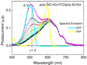
8 Detection of change in fluorescence between reactive cyan and the yellow fluorophores using a-SiC:H multilayer transducers ···104
8.1 Optical transducer configuration and operation ···104
8.2 Spectral sensitivity ···105
8.3 Transient photocurrent signals ···106
8.4 FRET approach ···109
8.5 Summary ···110
9 Conclusions ···110
10 References ···112
Chapter IV System simulator and computational methods for monolithic double p-i-n photodiode ···115
1. Introduction ···117
1.1 Hypothesis and approach ···117
1.2 A conventional receiver based on standard photodiodes ···118
1.3 Working principle ···120
2 Electrical model ···121
2.1 Two connected transistor model ···121
2.2 Electric model validation and physics ···122
3 Optoelectronic model ···127
XVII
4.1 Two stage active circuit ···134
4.2 Computational method ···135
4.3 Transfer characteristics ···136
4.4 Dynamics of a parallel bucket connection ···140
5 Model validation ···141
5.1 Influence of theapplied voltage ···141
5.2 Influence of the optical bias ···146
6 Conclusions ···149
7 References ···151
Chapter V Opto-electronic conversion applications ···155
1 Using Switches ···157
2 SiC multilayer photonic structures with self optical bias amplification ···158
2.1 Introduction ···158
2.2 Device configuration and operation ···159
2.3 Transfer function characteristics ···160
2.4 Optical bias amplification ···161
2.5 Encoder and decoder device ···163
2.6 Optoelectronic model ···166
2.7 Summary ···167
3 Photonic active filters based on SiC multilayer structures ···167
3.1 Introduction ···167
3.2 Photonic active filters ···167
3.3 Opto-electronic conversion ···171
3.4 Summary ···173
4 Light filtering effects ···174
4.1 Numerical simulation ···174
4.2 Short-pass, long-pass and reject band filters ···175
4.3 Summary ···177
5 Characterization of a monolithic device for detection of FRET signals ···178
5.1 Transfer function of each fluorescent optical signal ···178
XVIII
6 Conclusions ···183
7 References ···184
Chapter VI Optical communications strategies evaluation, conclusions and future research directions 187 1 Optical technologies strategies evaluation ···189
1.1 Introduction ···189
1.2 Where are we today? ···190
1.3 Out comings from the thesis ···193
2 An optoelectronic product innovation strategy ···194
2.1 Motivation ···194
2.2 Dissemination strategy ···195
2.3 Research ···196
2.4 Photonic vision building ···198
2.5 Future research directions ···199
3 Running projects ···201
3.1 Optical biosensor systems ···201
3.2 X-Ray flat-panel detector for Medical Applications ···203
3.3 Wavelength Division Multiplexing System for short range optical communications (WDM) ·204 4 The digital city of tomorrow ···206
4.1 Urban traffic control ···206
4.2 Polymer Optical Fibers in automotive networks ···209
4.3 Optical Fibers in house communications ···212
4.4 Conceptual Communication technologies ···214
4.5 Moving towards Next-Generation Networks ···215
4.6 Innovation strategy framework ···216
XIX
Figure 1.2 Laser Scanned Photodiode image acquisition layout. ... 8
Figure 1.3 a) LSP configuration in addition with the electrical model proposed b) A fraction of the electrical circuit used for simulation. c) Simulated and experimental image intensity, Im,18 for a 7.5 mm donut with a 2.5 mm inner hole. L=50 W/m2 and L=5 W/m2.... 10
Figure 1.4 J-V characteristics in dark and at 300K. ... 13
Figure 1.5 J-V characteristics under AM1.5 irradiation and 300K. ... 13
Figure 1.6 Spectral sensitivity with (dash) and without (solid) applied optical bias. ... 14
Figure 1.7 Depletion width (open) and iac(L)/iac(0) ratio (solid) dependence with L . ... 15
Figure 1.8 a) =iac(0)- iac(L) as a function of the applied bias for different image intensities. b) Image intensity as a function of L under reverse, forward and zero bias for.0 is the flux constant for each exponential fit (solid line). ... 16
Figure 1.9 a) Image intensity as a function of L b)The ac photocurrent for one dimension scans under forward, reverse and zero bias and a grayscale photo and fingerprint representations. ... 17
Figure 1.10 Current density as a function of the electrical bias under dark and under different wavelengths (L=10 µW/cm2). ... 18
Figure 1.11 Spectral response dependence on the applied voltage under steady state light conditions: (a) in dark,(b) red (650 nm); and (c) green (550 nm), L=10 µW/cm2 . ... 19
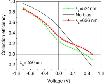
Figure 1.12 Collection efficiency as a function of the applied voltage in dark and under steady state light conditions. ... 20
Figure 1.13 a) Image intensity as a function of the electrical bias under different optical bias. b) A picture image of the sensor acronym CLSP with green “CL” and red “SP”. ... 21
Figure 1.14 Sensor element configuration. ... 23
Figure 1.15 I-V characteristics in dark and under red, blue and red&blue irradiation. ... 24
Figure 1.16 Schematic of the optically addressed device optimized for colour recognition. ... 25
Figure 1.17 Photocurrent as a function of the applied bias for sensors NC#4 (a) and NC#5 (b) in dark and under blue, green and red irradiation. (L=50µW/cm2). The inserts show, at the acquired applied voltages, the images from the same RGB picture (5). ... 26
XX
(solid lines)/recombination (dash lines) rates. ... 29
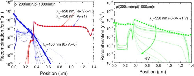
Figure 1.21 Electric field profile within the p-i-n/p-i-n tandem structure for different values of the external electrical bias and for different wavelengths of impinging light: a) 650 nm; b) 550 nm ; c) 450 nm d) thermo-dynamical equilibrium (dark). ... 30
Figure 1.22 Simulated potential profile under different applied voltages in dark and under red (L, =650 nm) green and blue (L, =450 nm) irradiation. ... 31
Figure 1.23 Potential drop across front (V1) and back (V2) diodes as a function of the applied voltage (V) and for different photocurrent values. ... 33
Figure 2.1 a-SiC:H WDM device configuration. On the top the recombination profiles (straight lines) under red (R =650 nm) green (G =550 nm) and blue (B =450 nm) optical bias and different applied voltages (-6V<V<0V). The generation profiles are also shown (symbols). ... 41
Figure 2.2 WDM device configuration (multiplexing mode). ... 42
Figure 2.3 WDM device configuration (demultiplexing mode). ... 42
Figure 2.4 Spectral photocurrent under: a) reverse bias (-5V) and different frequencies; b) different applied voltages and at a modulated frequency of 2000 Hz. ... 43
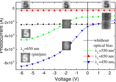
Figure 2.5 a) Spectral response at different applied bias. b) Photocurrent voltage characteristics under different light wavelengths. ... 44
Figure 2.6 Spectral photocurrent under different applied bias (a, c, e) and its trend with the applied voltage, at different wavelengths (b, d), for the front, p-i’ (a-SiC:H)-n, and back, p-i (a-Si:H)-n. ... 45
Figure 2.7 Spectral response at under negative and positive electrical bias. ... 46
Figure 2.8 ac IV characteristics under R (L =626 nm); B(L =470 nm), R(L =626 nm) & B (L =470 nm) modulated light and different light frequencies (15Hz;1.5KHz). ... 47
Figure 2.9 Transient multiplexed signals at different applied voltages and input wavelengths: a) R&B (R,B=626nm, 470 nm). The highest frequency of the input signal is 1.5 kHz. b) R&G&B (R,G, B=626 nm, 524 nm, 470 nm). The highest frequency of the input signal is 1 kHz. c) dependence of the input colour channel with the applied voltage d)
Transmission spectra of used red, green and blue signals. ... 48
XXI
a) R [00111100], G [01010010], B[00110011]; b): R [01111100], G [01010010], B[01010010]. On the top, the optical signal used to transmit the information guide the eyes on the different ON-OFF states. ... 50
Figure 2.13 Wavelength division multiplexing (solid lines) at – 5 V under different values of the modulation light frequency. The red and the green dashed lines guide the eyes into the input channels. ... 51
Figure 2.14 Multiplexed signals under negative and positive bias using two different bit rates: a) 2000 bps, b) 4000bps. On the top figure, the optical signal used to transmit the
information guide the eyes on the different ON-OFF states. ... 52
Figure 2.15 Photocurrent density variation with the optical bias measured for each optical channel (R: 626 nm, G: 524 nm and B: 470 nm) at -8 V (solid symbols) and + 1V (open symbols). The solid lines correspond to linear fits of the experimental data. Slopes (α)
of each plot are also displayed. ... 53
Figure 2.16 Transient multiplexed signals under negative and positive bias. a) Polychromatic red and blue time dependent mixture. b) Polychromatic red, green and blue time dependent mixture. The digital wavelength demultiplexed signal is displayed on the top of both figures. ... 54
Figure 2.17 Blue and red wavelength division demultiplexing output channels (dot lines) for the input signal (solid line) ... 55
Figure 2.18 Multiplexed signals under reverse and forward bias. On the top, the optical signal used to transmit the information guide the eyes on the different ON-OFF states. The bit sequence for the demultiplexed signal is shown for comparison. ... 56
Figure 2.19 a) Multiplexed experimental signal used for the calibration. On the top the input channels signals guide the eyes. b) A snapshot of the output from the MatLab routine used to demux the transmitted sequence of bits. The sequence of red, green and blue bits (shown at the top) was derived from the measured currents. ... 57
Figure 2.20 a) Multiplexed experimental signal used for decoding. On the top the input channels signals guide the eyes.b) A snapshot of the output from the MatLab routine used to demux the transmitted sequence of bits. The sequence of red, green and blue bits (shown at the top) was derived from the measured currents. ... 58
Figure 2.21 A snapshot of the output from the MatLab routine used to demux the transmitted sequence of bits. The sequence of red, green and blue bits (shown at the top) was derived from the measured currents. ... 58
XXII
(C&Y) irradiation... 61
Figure 2.25 Input channels (lines) and multiplexed signals (symbols) under negative and positive bias. ... 62
Figure 2.26 Multiplexed signal at -8V (symbols) and +1V (lines) under different optical power intensities of the cyan input channel and: a) different input channel frequencies. b) same input channel frequencies. ... 63
Figure 3.1 Device configuration . ... 72
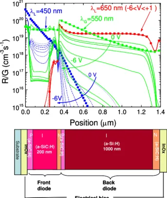
Figure 3.2 Recombination profiles (straight lines) under: a) red (R =650 nm) and blue (B =450 nm) b) green (G =550 nm) optical bias and different applied voltages. The generation profiles are shown (symbols). ... 73
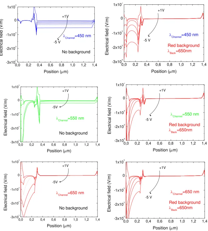
Figure 3.3 Electric field profiles within the p-I’-n/p-i-n tandem structure. a) under different wavelengths backgrounds (R,G,B) and without it, b) red background (R ) and
different color channels (chR, chG, chB). ... 74
Figure 3.4 Electric Field profile using the blue, the green, and the red channels without (left) and with (right) red optical bias. ... 75
Figure 3.5 Internal potential profile within the device under different light wavelength. Results are shown with and without external reverse bias. ... 76
Figure 3.6 Internal potential profile within the complete device under different light background wavelengths and without it. ... 77
Figure 3.7 Internal space charge profile within the complete device under different light wavelength. Results are shown under reverse bias and for different background
illumination. ... 78
Figure 3.8 Simulated spectral photocurrent under different background wavelengths. ... 80
Figure 3.9 Spectral photocurrent under reverse and forward bias measured with: a) Red, b) Green and c) Blue background illumination. ... 81
Figure 3.10 Spectral photocurrent @ +1 V, -8 V without (dark) and under red, green and blue optical bias. ... 82
Figure 3.11 Ratio between the photocurrents under red, green and blue steady state illumination and without it (dark). ... 82
Figure 3.12 Spectral photocurrent under positive (+1V) and negative (-8V) applied voltage and different frequencies without additional optical bias (a) or under steady state red (b), green (c) and blue (d) irradiations (background). ... 83
XXIII
frequencies. ... 86
Figure 3.16 Photocurrent variation with the wavelength for different frequencies at 8 V obtained: a) without, b) with red, c) with blue and d) with green background. ... 87
Figure 3.17 Spectral gain as a function of the frequency at 624 nm (red channel), at 526 nm (green
channel) and at 470 nm (blue channel) under red (αR), green (αG) and blue (αB)
backgrounds. a) short-pass filter , b) band-stop filter, c) long-pass filter. ... 88
Figure 3.18 Green (a), blue (b) and red (c) channels under negative (symbols) and positive (dot ... 89
Figure 3.21 Experimental color recognition using the WDM technique: a)6000bps. b)2000bps. ... 92
Figure 3.22 Schematic MUX/DEMUX diagram. ... 93
Figure 3.23 Single and combined signals @-8V; without (solid arrows) and with (dotted arrows) green optical bias. ... 94
Figure 3.24 Multiplexed signals at -8V/+1V (solid /dot lines); without (bias off) and with red, green and blue optical bias. ... 95
Figure 3.25 Multiplexed signal under obtained at reverse bias without optical bias (black line) and under steady state illumination of wavelength (light colored line): Left-524 nm and Rigth-470 nm. The difference between both signals is also plotted (dark colored line).96
Figure 3.26 Output waveform signal at -8V; without (φL=0) and with (R, G, B) optical bias. The bit
sequences are shown at the top of the figures. ... 97
Figure 3.27 Output waveform signal at -8V and +1 V; without (φL=0) and with (R) optical bias. ... 98 Figure 3.28 Output waveform signal at -8V; without (bias off) and with (R) optical bias. ... 99
Figure 3.29 (a) red (b) green and (c) blue channels under reverse and forward voltages without and with (L) red, green and blue steady state bias at 250 Hz and 2000 Hz, on top and down part of the figure, respectively. ... 101
Figure 3.30 Multiplexed signals with and without different backgrounds. On the top, the optical signal used to transmit the information. ... 102
Figure 3.31 Filtered output signals: a) red background. b) blue background c) green background. On the top, the optical signal used to transmit the information. ... 103
Figure 3.32 a) Optical transducer configuration. b) Fluorescence emission of glucose oxidase. ... 104
Figure 3.33 Spectral photocurrent under: a) reverse (-8 V) and b) forward bias (+1 V). ... 106
XXIV
Figure 3.36 Output photocurrent signals without (ФL=0) and with optical bias (624 nm, 470 nm, 400
nm) at: a) forward bias (+1 V) and b) reverse bias (-8 V). The optical signals waveforms are shown at the top of the figure. ... 108
Figure 3.37 a) Multiplexed signals with and without red background. b) Input channels with red irradiation and without it at -8V. On the top, the optical signal used to transmit the information. ... 109
Figure 4.1 Optoelectronic block diagram. ... 116
Figure 4.2 A schematic conventional RGB receiver. ... 118
Figure 4.3 A schematic functionality of a RGB receiver based on multilayered a-SiC:H p-i-n structures. ... 119
Figure 4.4 Input channels (R, G, B) and multiplexed signals (R&G&B) under negative (symbols) and positive bias (lines) applied bias. ... 120
Figure 4.5 Compound connected phototransistor equivalent model. ... 121
Figure 4.6 a) Equivalent electrical circuit of the pinpin photodiode. b) Signals obtained using SPICE simulation when the red (I2) and the blue (I1) modulated lights are impinging the device. ... 122
Figure 4.7 a) Equivalent electric circuit of the pinpin photodiode used in SPICE simulation. b) Voltage drop (VBE) across Q1 and Q2 under red (I2=20uA), blue (I1=12uA) and green (I3=10uA, I4=8uA) pulsed lights and negative and positive applied voltages. ... 123
Figure 4.8 Under red (I2=20uA), blue (I1=12uA) and green (I3=10uA, I4=8uA) pulsed lights and different applied voltages: a) Output signals. b) Current across the capacitors, I(IC1), I(IC2). ... 124
Figure 4.9 a) Equivalent electrical circuit of the pi’npin device used for electrical simulation
proposes. b) Voltage drop across Q1(symbols) and Q2 (lines). ... 125
Figure 4.10 ac equivalent circuit. ... 126
Figure 4.11 Block diagram of the state model considered as a parallel current bucket connection inflow [ // ]. ... 132
Figure 4.12 a) Two connected transistor model, b) Two active capacitive filter sections and c) ac equivalent circuit. ... 133
Figure 4.13 Block diagram of the optoelectronic state model for a pi´n/pin device. ... 134
XXV
Figure 4.17 The distribution and output of fluid volume inside communicating-vessels system visualize parallel bucket properties.a) positive voltage.b) negative voltage. c) front optical bias.d) back optical bias. ... 140
Figure 4.18 Multiplexed simulated (symbols), current sources (dash lines) and experimental (solid lines) under negative (R1=1K; -8V) and positive (R1=10M; +1V) dc bias without any background... 141
Figure 4.19 Multiplexed simulated (symbols) and experimental (solid lines) results under positive and negative dc bias. b) Photocurrent signals measured with different input channels under reverse (-8 V, solid arrow) and forward (+1 V, dotted arrow) bias. ... 142
Figure 4.20 a) Multiplexed signals under negative and positive bias. On the top, the optical signal used to transmit the information guide the eyes on the different ON-OFF states. b) Simulated (symbols) and experimental (lines) multiplexed signals (under positive (R1=10M; +1V) and negative (R1=1k; -8V) dc bias. The ac current sources used as input channels (dash lines) are displayed. ... 143
Figure 4.21 a) Input channels (lines) and multiplexed signals (symbols) under negative and positive bias. b) Multiplexed simulated (symbols) and experimental (solid lines) signals under positive (R1=10M; +1V) and negative (R1=1k; -8V) dc bias. The current sources used as input channels (I1 and I2) are displayed. ... 144
Figure 4.22 Multiplexed simulated (symbols), current sources (dash lines) and experimental (solid lines): under negative (R1=1k; -8V) dc bias and green (a) and red (b) backgrounds. .. ... 146
Figure 4.23 Output simulated waveform (symbols), current sources (dash lines) and experimental signals (solid lines), under negative (R1=1k; -8V) without and with red background. .... ... 147
Figure 4.24 a) Multiplexed signals with and without red background. b) Multiplexed simulated (symbols), input channels (dash lines) and experimental (solid lines): under negative dc bias and red background. ... 148
Figure 5. 1 a)Light emitting and sensor element (switch ON) b) Interruption of the light beam (switch OFF) c) Reflection light beam (switch ON) . ... 157
Figure 5. 2 Device design and operation. ... 159
Figure 5. 3 Photocurrent without and with front (a, c) and back (b, d) backgrounds.The current of the individual photodiodes are superimposed (dash lines). ... 160
XXVI
Figure 5. 7 a) Normalized red, green and blue transient signals at -8V with violet (400 nm) steady
state optical bias applied from the front side (αpin1) and from the back side (αpin2). b)
Input R,G,B channels and multiplexed output without (no bias) and under front (pin1) and back (pin2) irradiation. ... 163
Figure 5. 8 MUX/DEMUX signals under front and back irradiation. In the top, the RGB decoded information is shown. ... 164
Figure 5. 9 MUX signal under front and back irradiation. On the top the DEMUX signals obtained using the decoder algorithm is displayed as well as the binary bit sequences. ... 165
Figure 5. 10 Simulated (symbols) and experimental (solid lines) multiplex signals under front and back violet background. ... 166
Figure 5. 11 Spectral photocurrent without and under different background intensities and
wavelengths: red (a), green (b), blue (c) and violet (d) backgrounds. The optical bias is applied from the front (solid symbols) and from the back (open symbols) sides. ... 168
Figure 5. 12 Normalized spectral photocurrent under front (a) and back (b) violet irradiations with different intensities. ... 169
Figure 5. 13 Input red, green and blue transient signals at -8V without (no bias) and with: red (R), green (G), blue (B) and violet (V) optical bias from the front (pin1) and back (pin2) sides. ... 170
Figure 5. 14 MUX signal outputs and truth tables of the encoders that perform 8-to-1 multiplexer (MUX) function, under front (a) and back (b) violet irradiations (x means " not
significant"). ... 172
Figure 5. 15 A two-position opto-mechanical switch: a) Front violet background (Red ON, Blue OFF) b) Back violet background (Blue ON, red OFF). ... 173
Figure 5. 16 ASCA simulated recombination and generation profiles under front (a) and back (b)violet irradiation.Simulated electrical field profiles under front (c) and back (d)violet irradiation. ... 174
Figure 5. 17 Red (RCh), green (GCh) and blue (BCh) channel signals under: a) violet background from the front and back sides; b) front red and blue irradiations. ... 176
Figure 5. 18 Filtered output signals: a) front (lines) and back (symbols) violet irradiation. b) Front red, green and blue background. On the top, the optical signal used to transmit the information guide the eyes. ... 176
Figure 5. 19 Simplified schematic diagram of the structure of the device. ... 178
XXVII
chromatic sequences of Figure 5.21. The sequence of the input fluorescent signals (shown at the top) was derived from the measured currents. ... 181
Figure 5. 23 Output photocurrent with increasing optical intensities of the emission signals: a) cyan emission under back cyan background; b) yellow emission under front violet
background. ... 182
Figure 5. 24 Output photocurrent signals with different optical intensities of the yellow/cyan emission signals: a) cyan emission under back optical bias of cyan background; b) yellow
emission under front optical bias of violet background. ... 182
Figure 6. 1 Multi-disciplinary technologies for infrared telecommunication systems, capacity, distance and functionality versus the cost per bit rate. ... 190
Figure 6. 2 Erbium-Doped Fiber Amplifier Design ... 191
Figure 6. 3 WDM Transmission System. ... 192
Figure 6. 4 Dissemination Strategy ... 195
Figure 6. 5 Schematic diagram of the transducers essays. An indoor, line-of-sight visible light communication link. ... 196
Figure 6. 6 POF and pi’n/pin a-SiC:H device: a memory element of a “light computer”. ... 198 Figure 6. 7 llustration of a standard traffic control system ... 206
Figure 6. 8 Lighting sources can be used for background irradiation, data communication and infrastructure lightings simultaneously ... 207
Figure 6. 9 An illustration of traffic control system of tomorrow ... 208
Figure 6. 10 Competing communication technologies, distance and applications. ... 209
Figure 6. 11 Loss spectrum of optical fibers. ... 210
Figure 6. 12 Future Automotive Networks with POF and repair shop infrastructure ... 211
Figure 6. 13 Driver’s door module with various switches. ... 211 Figure 6. 14 Conceptual illustration In House Communication: a) FTTx solutions; b) FTTCab “Fiber
to the Cabinet” scenario, ... 212 Figure 6. 15 Conceptual illustration In House Communication FTTH_ Fiber to the Desk (FTTD)
using plastic optical fiber to reach office equipment. ... 213
XXVIII
217
XXIX
Table 1.2 Optoelectronic characteristics for the amorphous LSP sensors ... 12
Table 1.3 Deposition conditions of the a-Si:H and a-SiC:H films. ... 24
Table 5.1 Gains (αR, G,B,V
XXXI
A Area of the diode
AC Alternate current
APD Avalanche Photo Diode
ASCA-2D Device simulation program
a-SiC Amorphous Silicon Carbide
a-SiC:H Hidrogenated Amorphous Silicon Carbide
a-Si:H Hidrogenated Amorphous Silicon
AWG Arrayed Waveguide Grating
ADSL Asymmetric Digital Subscriber Line
ATM Asynchronous Transfer Mode
B Blue
C Carbon
CCD Charge Coupled Device
CFP Cyan Fluorescent Protein
YFP Yellow Fluorescent Protein
Chap. Chapter
CID Charge injecting devices
CWDM Coarse Wavelength Division Multiplexing
CMOS Complementary metal oxide semiconductor
CN Core network
C-V Current-voltage measurements
C-V Capacitance-voltage
DC Direct current
DEMUX Demultiplexer
DWDM Dense Wavelength Division Multiplexing
DSLAM Digital Subscriber Line Access Multiplexer
EDFA Erbium Doped Fiber Amplifier
EoPOF Ethernet over Plastic Optical Fiber
FET Field effect transistor
FBG Fiber Bragg Grating
FRET Fluorescence Resonance Energy Transfer
FTTB Fibre To The Building
FTTC Fibre To The Curb
XXXII
FTTx Fibre To The x
G Green
GPS Global Positioning System
GSM Global System for Mobile Communications
ICP – ANACOM Portuguese telecommunication regulators authority
IMS IP-based Multimedia Services
IP Internet Protocol
Iph Photocurrent
IP-TV Internet Protocol Television
ITO Indium Tin Oxide
In Indium
IR Infra-red
IS Saturation current
I-V Current-voltage
J-V Density current-voltage
LASER Light Amplification by Stimulated Emission of Radiation
LCD liquid crystal display
LED Light Emitting Diode
LSP Laser Scanned Photodiode
NGN Next Generation Networks
MUX Multiplexer
OADM Optical Add-Drop Multiplexer
OXCs optical cross connects
PECVD Plasma Enhanced Chemical Vapour Deposition
PIN Positive-Intrinsic-Negative
POF Plastic Optical Fiber ou Polymeric Optical Fiber
q Electronic charge
R Red
RF Radio frequency
RGB Red, Green, and Blue
SDH Synchronous Digital Hierarchy
SiH4 Silane
S/N Signal to noise ratio
s Spectral responsivity
XXXIII
VIS Visible
Voc Open circuit voltage
W Width of space charge region
WDM Wavelength-Division Multiplexing
VT Thermal voltage
Incident radiant power
XXXV
Symbol
Units
Description
A cm2 Area of the junction
α cm-1 Absorption coefficient
Dp cm2s-1 Diffusion coefficient for holes
Dn cm2s-1 Diffusion coefficient for electrons
εs Fcm-1 Dielectric constant of the semiconductor
Eop eV Optical gap
Eg eV Energy gap
φ cm-3s-1 Light flux
Gop cm-3s-1 Optical generation
h Js Planck’s constant
Iph A Photocurrent
I0 A Dark current
s-1 Frequency
η % Quantum efficiency
λ nm Wavelength
ND cm-3 Density of ionized defect states
Na cm-3 Doping concentration of the p-layer.
Nd cm-3 Doping concentration of the n-layer
Popt W Optical power
q C Electron charge
R % Reflection coefficient
ℜ A/W Responsivity
Vbi V Built-in potential
V V Applied voltage
T K Absolute temperature
τp s-1 Lifetime of holes
τn s-1 Lifetime of electrons
W m Depletion region width
EF eV Energy of the Fermi level
EV eV Top edge of the valence band
EC eV Bottom edge of the conduction band
k eV K-1 Boltzmann constant
μn cm2V-1 s-1 Electron drift mobility
μp cm2V-1 s-1 Hole drift mobility
σph Ω-1cm-1 Photoconductivity
σD Ω-1cm-1 Dark conductivity
σL Ω-1cm-1 Conductivity under illumination
E eV Energy
XXXVII Three Real-time Visible Light Memories…
I suppose the first time I really appreciated the combination of light and control was as an adolescent watching my neighbour “Miguel Fogueteiro” with his exciting fireworks: It was demanding attendance the traditional cyclist, with special effects changing colour every minute and in “perfect synchronization”
with the pyrosounds and animated magic illusion displays. I had never seen anything like it, and I was amazed by the visual impact caused by the Almeida´s pyrotechnical shows.
Urban traffic control systems are remarkable systems to combat city centre congestion, a key element in the efficiency of urban mobility and sustainable development policy. Faced with the growth in vehicle traffic, it ensures higher fluidity, thereby reducing fuel consumption, traffic jams and resulting nuisances (noise and CO2 pollution). In the Lisbon case, for example, the urban traffic control management has
produced in the near past a 50% reduction in journey time, savings of 35% in fuel, and a 70% decrease in vehicle pollution.
My fascination with the traffic lights began later on, when I became a traffic engineer in Lisbon´s municipality: the state of all local traffic lights could be changed every second!
During the last years I have been fascinated by WDM control: the visible light that pulses as a
millisecond signal transmitter and the appropriate controlled device acting as a receiving component
XXXIX
Problem introduction
“The development of an integrated device, at low cost, able to be used as a multiplex/demultipex
device in the visible range for short range communication”.
The increased use of electronics in automobiles has seen the installation of multiple networks in modern cars, and the expansion of these systems has quickly accelerated. It is now believed that the amount of information that will need to be transmitted in the field of automobile technology will increase rapidly in the near future, in information (in-car navigation, DVD´s), in control and safety systems and in body systems (switches, actuators). Since 1998 Europeans car makers have adopted optical fibers networks. The emergence of WDM is one of the most recent and important phenomena in the development of fiber optic transmission technology. So an increase in network data rates is urgently required.
XL
“Which kind of amorphous Si/SiC transducers, with low cost and appropriated transmission rates should be developed to allow the recovery, or routing of specific wavelengths for the transmission over WDM networks, in the visible spectrum, that could compete with conventional detection electronic devices in optical communications industry?”
This research question defines the thesis proposal and guides our arguments and study. It demands innovative approaches to the exploration of problems, involves a new methodology, a new conceptual approach and clearly demonstrates their relevance to society, contributing to the goals of sustainable development.
Hypothesis and approach
It is known that in order to enhance the transmission capacity and the application flexibility of optical communication and sensor systems different tasks have to be considered, namely:
-The use of Wavelength Division Multiplexing (WDM) devices when different optical signals are encoded in the same optical transmission path.
-The design of active filter circuits by combining the properties of high-pass and low-pass into a band-pass filter.
There has been much research on semiconductor devices as elements for optical communication when a band or frequency needs to be filtered from a wider range of mixed signals. Amorphous silicon carbon tandem structures, through an adequate engineering design of the multiple layers’ thickness,
absorption coefficients and dark conductivities can accomplish this function. The advantages of this approach are the feasibility of large area, the deposition on different substrate materials (glass, polymer, etc.), the simplicity of the device design and associated electronics, the high resolution, uniformity and the cost/simplicity of the detector. It can also be integrated vertically on top of a read-out electronics, which enables low cost large area detection systems where the signal processing can be performed by an ASIC chip underneath.
So an example of hypothesis in this optoelectronic area of research could be:
“In the visible range, integrated Wavelength-Division Multiplexing /Demultiplexing devices can be achieved at low cost and competitive transmission rates if multilayered p-i’-n-p-i-n heterostructures, produced by PECVD, are used as electrically programmable optical active filters with light triggering
XLI
The opening chapter introduces many of the basic principles of the emerging technologies of photonic switching and optical signal processing. We have tried to make some kind of review and acquisition of knowledge on photo-sensing devices using a-SiC based learning materials. We hope first, to provide an overview of amorphous silicon material properties from the early groups, on the optoelectronic characterization, light-to-dark sensitivity, optical amplification, laser scanned photodiode (LSP) technique and ending with the dilemmas of self- field induced depletion layers for light detection in color and image transducer.
Second chapter deals with voltage controlled devices, in different multilayered a-SiC:H pin architectures, are compared and optimized to be used as multiplexing and demultiplexing devices in
the visible range. A double pi’n/pin a-SiC:H heterostructure with two optical gate connections for light triggering in different spectral regions is presented. Multiple monochromatic pulsed communication channels, in the visible range, are transmitted together, each one with a specific bit sequence. The combined optical signal was analyzed by reading out the generated photocurrent across the device, under positive and negative applied voltages. The transducers are also optimized to provide the high-sensitivity needed for low-light applications such as fluorescence.
In third chapter, a pi’n/pin a-SiC:H voltage and optical bias controlled device is presented and its behaviour as image and colour sensor, optical amplifier and demux device discussed. The design and the light source properties (wavelength, intensity and frequency) are correlated with the sensor output characteristics (light-to-dark sensitivity, resolution, linearity, bit rate and S/N ratio). Different readout techniques are used. When a low power monochromatic scanner is used to readout the generated carriers by the scanner, the transducer recognize a color pattern projected on it, acting as a color and image sensor. If the photocurrent generated by different monochromatic pulsed channels is readout directly, the information is demultiplexed. Finally, when triggered by appropriated light, it can amplify or
suppress the generated photocurrent working as an optical amplifier. SiC pi’npin wavelength selective
channel filters optimized for a fine tuning of different wavelengths are analyzed. Optically switchable on SiC multilayer photonic structures based on a short- or a long- pass band active filter or as a band-stop active filter are analyzed.
In the forth chapter based on the experimental results and device configuration (chapters II and III), an optoelectronic model is developed and supported by an electrical simulation. A demux algorithm is implemented. The first step was to determine the dc biasing condition for each stage, followed by ac analysis using the proper equivalent circuits. The ac circuit representation is supported by the complete dynamical large signal Ebers-Moll model with series resistances and capacities. The Kirchhoff’s laws
XLII
The purpose of fifth chapter is to present a new reconfigurable logic architecture that offers considerable improvements in sensing, measurement, manufacturing and opto-electronic conversion applications. Combined tunable converters based on SiC multilayer photonics active filters are analyzed. MUX signals that perform 8-to-1 MUX function and truth tables lookup are compared. A decoding algorithm was implemented and tested.
Chapter I
Background theory on a-Si/SiC photodiodes
I
scn
i
p
i
ph
-Scanner
Image
1/r
d ~I
phR
LnAl
R
Lp D3
Introduction
This opening chapter introduces many of the basic principles of the emerging technologies of photonic switching and optical signal processing. Optical computing has a long and diverse history. In the future network, optical technology will play a stronger role not only for transmission but also for switching. Optical filters play important roles in communication systems. The further development of core and photonic technologies (photodetectors, optical amplifiers, transmitters and receivers, multiplexers, cross-connects, and sensors), will be fundamental in strategic applications such as medicine, communications, lighting, sensing and measurement, and manufacturing. We have seen that photonic signal processing is a key enabling technology for faster transmission, switching and control. The current trend in photonic signal processing is clearly toward integrated solutions.
We have tried to make some kind of review and acquisition of knowledge on photo-sensing devices using a-SiC based learning materials. For it, we have distilled the essence of the team knowledge, seeking to create a picture of Amorphous Si/SiC photodiodes used in different applications: Laser Scanned Photodiode black and white Image sensors, LSP image and color transducers, and Si/SiC tandem photodiodes.
We wish to do more than provide a transcription of what was done. We have set the context for the rest of this dissertation.
In order to enhance the basic requirements of the system architecture, the transmission capacity of experimental design, the simulating parameters in the optoelectronic algorithm interface and the application flexibility of optical communication and sensor systems in visible spectrum, different tasks have to be considered. We hope first, to provide an overview of amorphous silicon material properties from the early groups, on the optoelectronic characterization, light-to-dark sensitivity, optical amplification, laser scanned photodiode (LSP) technique and ending with the dilemmas of self- field induced depletion layers for light detection in color and image transducer.
1. Current state of art on Amorphous Si/SiC photodiodes.
Amorphous Si/SiC photodiodes working as photo-sensing or wavelength sensitive devices in the visible range, have been widely studied in the past for different application (solar cells, color sensors, image sensors).
4 the growth of amorphous silicon from plasma of silane by Chittiwick et al [1]. An important advance occurred in 1975, with the demonstration of substitutional doping by Spear e LeComber [2].
In early studies of amorphous silicon, it was determined that plasma-deposited amorphous silicon contained a significant percentage of hydrogen atoms bonded into the amorphous silicon structure. When amorphous silicon is deposited under hydrogenation conditions the hydrogen atoms binds to dangling bond defects and removes the corresponding electronic states in the band gap, which eliminates most of the trapping and recombinations centers. This process of introducing hydrogen into silicon is usually designated as passivation of the dangling bonds. These atoms were discovered to be essential for the improvement of the electronic properties of the material. Amorphous silicon is generally known as “hydrogenated amorphous silicon”, or a-Si:H. Hydrogenated amorphous silicon (a-Si:H) has a sufficiently low amount of defects to be used within devices. However, the hydrogen is unfortunately associated with light induced degradation of the material, termed by the Staebler-Wronski Effect [3].
Amorphous alloys of silicon and carbon (also called amorphous hydrogenated silicon carbide, a-Si1-xCx:H) are an interesting variant to this material. The introduction of carbon adds extra freedom to control the properties of the material. Increasing concentrations of carbon in the alloy widen the electronic gap between conduction and valence bands (also called "optical gap" and bandgap), in order to potentially increase the light efficiency of solar cells made with amorphous silicon carbide layers. On the other hand, the electronic properties as a semiconductor (mainly electron mobility), are poorly affected by the increasing content of carbon in the alloy, due to the increased disorder in the atomic network.
While a-Si suffers from lower electronic performance compared to crystalline silicon (c-Si), it is much more flexible in its applications. It may also produce savings on silicon material cost, as a-Si layers can be made thinner than c-Si.
5
2. Amorphous pin photodiodes
2.1 The physics of the p-i-n photodiode
2.1.1 Uniform illumination
As already mentioned the absorption of radiation is caused by the interaction of photons and charge carriers inside the material. The different allowed energy levels and the band structure determine the possibility of interaction and, therefore, the absorption characteristics of the semiconductor. Light is also capable of inducing conduction electrons and holes in the silicon. Photons with energy higher than the optical gap are absorbed by the material and generate conduction charge carriers (electrons and holes) by converting valence electrons to conduction electrons. Measurement of electron-hole density gives a measure of the intensity of the light falling on the semiconductor. This is commonly achieved through the use of the diode structure. Electron-hole pairs generated in the depletion region find themselves in an electrical field and are immediately collected. Those generated outside the depletion region diffuse inside the field-free semiconductor (along a concentration gradient) until they either recombine, or fall under the influence of the electric field in the depletion region. The collected carriers contribute to the photocurrent, resulting in an electrical current through the external load or without load, in an external voltage at the contact terminals, the so called open circuit voltage, Voc. The
equilibrium is established between the generation, the recombination of carriers, and the current flow through the load. To achieve high efficiencies, as many carriers as possible should be collected by the electrical field inside the space charge region. The width, W, of the space charge region is a function of the doping concentration and on the applied voltage. For one side abrupt junction [4]:
B bi s
qN
V
V
W
2
(1.1)where Vbi is the built-in voltage, s the dielectric constant of the semiconductor and q the electronic
charge. The speed limiting capacitance of the diode is also a function of the space charge width and is given by:
A
W
C
s (1.2)where A is the area of the diode. Diodes based on p-i-n structures show a larger space charge width when compared with the p-n due to the lower doping level of the intrinsic layer.
6 strongly proportional to the incident radiant power (i). The ratio of both variables defines the spectral
responsivity (s). The characteristics of the irradiated photodiode are then given by:
ph T
D S
D
I
V
V
I
I
exp
1
(1.3)with ISthe saturation current, the ideality factor of the diode, and VT the thermal voltage.
For large signal or dc mode, the photodiode can be described as a non-linear current source, ID,
feeding into an ideal diode, and its internal characteristics are better modeled by the introduction of a shunt resistor, a shunt capacitor and a series resistor [5]. Under small-signal conditions or ac mode, the photodiode behaves as a non-linear photocurrent-controlled resistor (rd), which represents an
incremental resistance, around the quiescent operating point, and is expressed in terms of Iphas:
T ph D D
d
V
I
V
I
r
1
(1.4)
2.1.2 Non-uniform illumination
As mentioned before the uniform illumination of a p-i-n junction leads to the appearance of a transverse photovoltage between the two sides. If the illumination is not spatially uniform, due to the carrier gradient between irradiated and dark regions, an additional effect arises resulting in a lateral photovoltage parallel to the junction, Vph,l in addition to the transverse one, Vph,t.. Due to the higher conductivity of the doped layers, the photogenerated minority carriers build up across the doped layers, while the majority carriers are accumulated in the illuminated region, beyond the depletion layer edge, causing a reduction in the band bending across this region. A deviation from the carrier density equilibrium occurs resulting in lateral drift and reinjection of minority carriers (holes from the p-side and electrons from the n-side) into the intrinsic layer where they are trapped instantaneously as reported in Figure 1.1.
The density of reinjected carriers depends on the resistivity of the intrinsic and doped layers and on the charge density of the i-layer[6, 7]. This anisotropic spatial distribution is responsible by an electric field modulation across the depletion region [8]. At the illuminated regions the electrical field is reduced, the depletion width shrinks (Equation1.1) and the capacitance increases (Equation 1.2). So, low local electric fields are ascribed to illuminated regions and high electric fields to dark zones.
7
i (a-Si:H)
Depletion region
Depletion region
TCO
TCO
p (a-SiC:H)
n (a-SiC:H)
Incident Light
Electrons Holes
Figure 1.1 Physical structure of a p-i-n photodiode under a light pattern illumination.
2.2 Laser Scanned Photodiode (LSP) image sensor
2.2.1 Solid state imagers
Whether we hope to view images or count photons, we use devices that work by absorbing photons and turning them into information. Traditional optics has relied heavily on the human eye for the evaluation of light distributions, using photographic films as an intermediate storage medium, when necessary. With the advent of computers and digital image processing, electronic image sensors have become indispensable tools. Three forces directed the evolution of image sensors: Advances in technology determine what is possible, algorithms determine what is practical, and applications determine what is desirable. If we wanted to generalize about areas in which detectors and imaging technology can improve, we could talk about collecting information more quickly and efficiently, at more wavelengths, with more compact and user-friendly devices or interfaces.
Any conventional solid state imaging device consists of an array of sensing elements combined with some form of transport mechanism to deliver the sensor output signal to the periphery of the device. Sensors used in commercial devices include photodiode arrays [10, 11], charge-coupled device (CCD) [12, 13], complementary metal oxide semiconductor (CMOS) [14], charge injecting devices (CID) [15], and bipolar transistors [16]. All of these devices use essentially the same light sensing mechanism. Photons penetrating a depletion region generate electron-hole pairs. These carriers are swept away by the electric field across the depletion region and generate a small transverse photocurrent. Except under very bright conditions, it is not possible to use this photocurrent directly. Thus, in order to achieve a reasonable signal-to-noise ratio, these currents are usually integrated to produce an accumulated charge output.
8 light pattern [7, 17, 18]. Low local potential barriers are ascribed to illuminated regions and high potential barriers to dark zones [19]. Based on this effect, microcrystalline [20] and amorphous [21] optical TCO/p-i-n/metal image transducers were developed. Those sensors are fundamentally different from the CCD’s or from vacuum tube imager [22] systems as they are based on one single sensing element and use a modulated, low-power beam of laser light to “paint” the image directly.
2.2.2 Theory of operation and image representation
The Laser Scanned Photodiode is fundamentally different from the above described electrically scanned image systems. The main advantage is the simplicity of the structure; no special photolithography techniques for patterning or high voltage requirements and bulky design are needed. Figure 1.2 depicts the layout of image acquisition experiment.
A focused image, constituted by a steady-state light, is projected onto a fixed location in the photosensitive surface, through the transparent contact. For image acquisition, a low-power chopped laser spot scans the sensor in the raster mode.
Image retrieve starts with the front-end electronics, which receive and process signals from the sensor to a display system. The read-out of the injected carriers is achieved by measuring the ac component of the short circuit current, Isc. The processed signal contains the information about the light intensity in
each position of the sensor.
Sensor Laser (scanner) X mirror
Mask
Laser (image)
Y mirror (scanning)
Sensor Laser (scanner) X mirror
Mask
Laser (image)
Y mirror (scanning)
Figure 1.2 Laser Scanned Photodiode image acquisition layout.
It was shown that the output signal depends on the photocurrent produced by the image, Idc, as much
as by the one produced by the scanner, Iac [23]. This component can be analytically described by the
Equation 1.5 [4
]
, where R(L) is the small signal responsivity at a given illumination L,S(t) is theaverage power density of the moving scanner beam and d its diameter.
4
)
(
2
d
t
R
i
ac L S
9 The signal-to-noise power ratio (S/N) depends on both components of the current (I=iac+IDC) and is
given by Equation 1.6, where f is the bandwidth and R0 the sensor resistance at zero voltage bias.
f
I
q
R
kT
i
N
S
DC ac
)
.
2
4
(
02
(1.6)
The current is amplified by a current to voltage converter with selectable gain and converted to digital format by a signal acquisition card installed on a computer. A mxn grid with 200m x 250m spacing in x and y directions is used for image representation. All the scanning process is controlled by a microcomputer which stores the currents as a two dimensional array of discrete values, Im,n, each one
representing the photocurrent induced by the chopped light at the selected position. The data are stored as a matrix of photocurrent values which provide information about local illumination conditions on each position of the device active area. In order to get the effect of the image on the current distribution across the transducer and to outline its shape the image intensity, Xm,n, is obtained by
subtracting the input matrix Im,n(with image) from the background,
b
m,n (without image), Xm,n =-(Im,n-n m
b
, ).The Laser scanning methodology is explained by the junction electrical field modulation under non-uniform illumination. The optical mapping of the scene onto the sensor surface leads to a reduction of the electrical field at the illuminated regions and to a reduction in the depletion region. If, in addition, a weak light spot is scanning the device, in the dark regions the carriers generated by the probe beam are separated by the junction electric field and collected (high ac component of the current). Those generated inside the illuminated regions can drift in the lateral direction, due to the local lowering of the potential barrier, and recombine inside the amorphous bulk (low ac component of the current). So, illuminated regions are ascribed to low ac components of the photocurrent, and dark regions to high ac photocurrent values.
2.3 Electrical model and simulation
The p-i-n image sensor was modeled as an array of photodiodes interconnected through lateral resistors. In the ac mode, each photodiode (D) was replaced by its incremental resistance (rd) and
connected to its four neighbors, in a row-line matrix, by the resistors RLn and RLp that model the sheet