Built-in Self Test of High Speed Analog-to-Digital
Converters
Edinei Santin, Luis B. Oliveira, and Joao Goes
Signals found in nature need to be converted to the digital domain through analog-to-digital converters (ADCs) to be processed by digital means [1]. For applications in communication and measurement [2], [3] high conversion rates are required. With advances of the CMOS technology, the conversion rates of CMOS ADCs are now well beyond the gigasamples per second (GS/s) range, but only moderate resolutions are required [4]. These ADCs need to be tested after fabrication and, if possible, during field operation. The test costs are a very significant fraction of their production cost [5]. This is mainly due to lengthy use of very expensive automated test equipment (ATE) to apply specific test stimuli to the devices under test (DUT), and to collect and analyse their responses.
With high conversion rates it is difficult to interface the ADCs to the test instruments due: extra parasitics, line trace mismatches, interferences within the printed circuit board (PCB), and the instrument test probes. This becomes even more challenging in the case of systems-on-a-chip, system-in-a-package, and three-dimensional (3D) chips, where the accessibility of the ADCs for testing purposes is restricted [6].
In this paper we discuss the use of built-in self-test (BIST) techniques for testing high speed ADCs and we present a specific solution, in which the analog input signal and the clock are generated internally.
BIST for High Speed ADCs
Using advanced CMOS technologies, the cost per transistor decreases and integrated solutions become competitive. Thus, more specific functionalities can be fully integrated on-chip. Moreover, the reliability of the manufacturing process maintains high, allowing reliable function to be implemented on-chip as well.
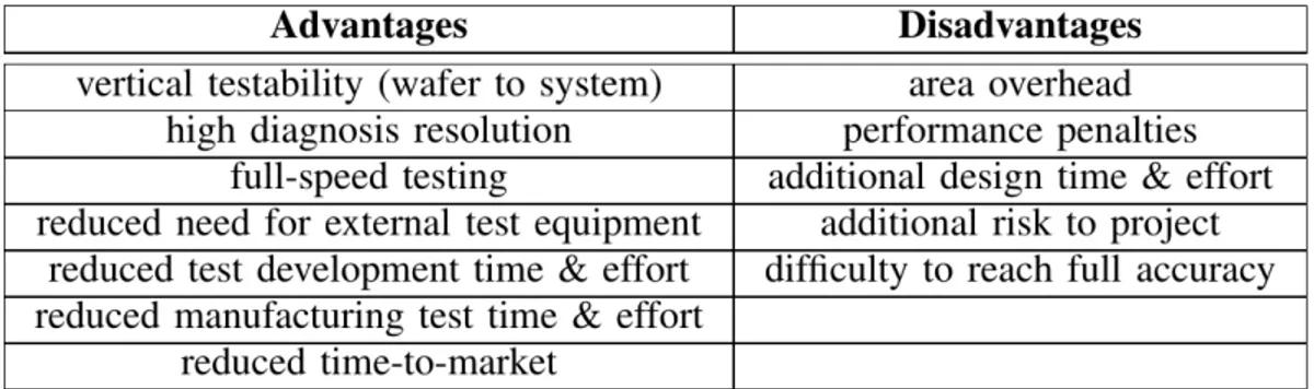
The implementation of test-related functions directly on-chip during the IC design phase, which is called design for testability, evolved firstly for purely digital ICs and then migrated to mixed-signal devices. Using a BIST approach contributes to additional area, increases design time and effort, and may degrade the performance of the DUT due to intrusive test structures.Table 1 summarizes the pros and cons of a BIST solution.
Table 1 - Summary of advantages and disadvantages of BIST.
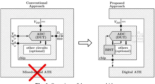
As discussed above, as a result of the increase of the conversion rate of ADCs, from the present few GS/s, their testing becomes progressively more time-consuming and costly. Here we present a novel solution, which consists of using two small area synchronized phase-locked loops (PLLs) to generate high frequency sinusoidal and clock signals. We analyse the possibility of using a dedicated BIST approach for testing high speed, moderate resolution ADCs, either embedded into complex systems or as standalone components. This BIST approach is based on two compact and easy-to-integrate oscillators that generate high frequency test stimuli (analog input and clock) to the DUT. Instead of using free-running oscillators for generating the analog input and clock test stimuli, we propose to employ two phase-locked-loops to improve the phase noise of the generated signals and, more importantly, to allow coherent sampling. The use of coherent sampling is beneficial since it simplifies the processing of the output data and a coherent sampled signal leads to a coherent spectrum, which avoids undesirable artefacts due to spectral leakage. This fully integrated in CMOS technology BIST approach, which reduces test costs by avoiding the need of expensive mixed-signal ATEs, improves reliability by avoiding interfacing critical signals between the DUT and ATE, and enhances feasibility by carrying out the test procedure completely on-chip, is the main contribution of this paper. Although the DUT used in this work employs a pipelined ADC topology, the approach can be applied to other converter topologies, since it “sees” the DUT as an almost ideal “black box”. The conceptual overview of the proposed approach is shown in Fig. 1.
Fig. 1. Overview of the proposed idea.
Using the proposed BIST approach, the only off-chip component required is a low frequency and stable reference signal. Digital signal processing (DSP) techniques for output response analysis are used, which rely primarily on spectral computations using fast Fourier transform (FFT) algorithms. The proposed concept was implemented in an integrated circuit featuring two PLLs for test stimuli generation and an 8-bit 500 MS/s ADC as the DUT and was validated with silicon measurements. In a 0.13 µm CMOS technology, the area overhead introduced by the two PLLs is only 0.052 mm2.
PROPOSED ADC BIST ARCHITECTURE
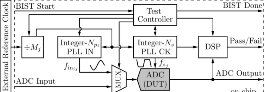
The ADC BIST architecture proposed in this work is illustrated in Fig. 2. It is composed of two
integer-N PLLs (PLLIinteger-N and PLLCK) that share the same external reference clock to ensure signal
synchronization. This synchronization is necessary to achieve coherent sampling. PLLIN generates low distortion, high frequency, and low jitter sine wave signals, while PLLCK generates high frequency and low jitter square wave clock signals, which are used to drive the ADC during the test procedure. The only off-chip component required is a stable and low frequency reference clock, which may be implemented, for example, by an inexpensive crystal oscillator. The digitized samples are processed by a DSP (e.g. to execute a FFT algorithm), in order to calculate the most important functional performances of the DUT. The results may then be compared, for example, with different effective resolution thresholds (e.g. 6, 7, and 8 bits) up to the maximum resolution allowed by the self-testing system and, for each comparison, a pass or fail indication shown. With this, ADCs having different resolutions are sorted and it becomes possible to check the performance degradation during the ADC life time. A test controller takes care of the test application and sequence.
Fig. 2. Proposed BIST architecture for coherent testing of high speed ADCs.
When the two PLLs are locked, the input and sampling frequencies of the ADC are, respectively,
in p ref (1)
s s ref (2)
where fref is a stable external reference frequency, Ns is the number of collected samples, and Mj and Npi
(i,j = 1,2,...) are integer programmable frequency divider values, which enable different frequencies for the input and sampling signals. From Eqs. (1) and (2) coherent sampling is achieved (i.e. fin/fs = Np/Ns).
The architecture parameters Ns, Npi, and Mj are selected according to the resolution of the ADC under
test, the external reference frequency, the desired sampling frequencies (fˆsj), and the desired normalized
input frequencies (fˆini/fs). Ns is a power of two ideally given by Ns > π2N ≈ 2N+2 [7], where N is the number
of bits of the ADC. Npi (i = 1,2,...) is given by
p in s (3)
where {x} means the nearest odd integer value of x. Note that odd integer values for Npi ensure
irreducibility with respect to Ns, since the latter is a power of two (this irreducible ratio is another
requisite of coherent sampling). Mj (j = 1,2,...) is given by
ref
(4)
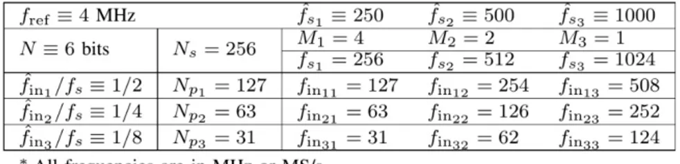
where is the nearest integer value of x. As an example, Table 2 gives the architecture parameters and the resulting frequency map for a hypothetical 6-bit ADC with fref = 4 MHz, fˆsj = 250, 500, and 1000 MS/s,
and fini/fs = 1/2, 1/4, and 1/8. We can see that the actual analog input and sampling frequencies are slightly
different from the desired ones, but this is required to guarantee coherent sampling.
Table 2 – Programmable parameters and frequency map for a 6-bit ADC.
The reconfigurable BIST architecture shown in Fig. 2 can be efficiently integrated (e.g. with small area overhead), as detailed explained in [8]. As a result, it is a very attractive solution for functional testing of high speed ADCs.
EXPERIMENTAL RESULTS
We will consider two extreme evaluation modes:
i) ADC driven by the external analog input and clock (this mode assesses the standalone ADC
performance); ii) ADC stimulated with the internal analog input and clock (this mode assesses the performance of the whole BIST system, i.e., ADC + PLLCK + PLLIN).
The test modes above are evaluated using the PCB board (with a wire-bonded die) shown in Fig. 3. The evaluation mode where both the analog input and clock are generated externally is the most demanding in terms of test equipment resources.
Fig. 3. Photograph of a wire-bonded die before glob top encapsulation (a) and of a completely assembled test board (b). Die dimensions are 1525×1525 µm2. PLLIN core occupies an area of only 138 µm ×282
µm and PLLCK occupies 92 µm ×138 µm.
The high-quality (i.e., very low phase noise) external analog input is provided by an RF signal generator, Marconi Instruments 2041. In order to remove the harmonics of the generated signal (intrinsic to this kind of generator), the analog input is bandpass or low-pass filtered before being applied to the test board. In this work, the following Mini-Circuits passive filters were used: SBP-10.7, 100+, 250+, SLP-550+, and SLP750+. The external clock signal, both for ADC clocking or for the reference clock of the PLLs, is provided by another RF signal generator, Rohde&Schwarz SMB100A/SMB-B112. This generator also has very low phase noise. For instance, the integrated rms jitter in the bandwidth from 100 Hz to 2 GHz at 1 GHz is merely 210 fs. The ADC output data are captured with a logic analyzer, Agilent 16702B/16715A, and the data are then remotely transferred to a personal computer and processed in MATLAB. A set of on-board push-button switches allows the configuration of the system and the selection of the desired test mode.
The standalone performance of the ADC, when both the analog input and the clock are provided externally, is presented. Following that, the whole ADC BIST performance is presented, when the analog input and the clock are both generated internally by PLLIN and PLLCK, respectively.
The results are presented in terms of the performance parameters: SINAD, SNR, and THD. Since the ADC topology is based on a two-channel time-interleaving (TI) array, it is also interesting to analyse the spurious tones caused by TI. The THD values presented account up to the 13rd harmonic. The even harmonics are insignificant with respect to the odd ones due to the use of differential signalling and very symmetrical and careful layouts. All results presented are derived from 512 collected samples, coherent spectra and no averaging is applied.
DUT with External Analog Input and Clock:
In this case the converter is stimulated with external analog input and clock. This evaluation gives a reference performance which can then be contrasted with the other evaluation case, in which the analog input and clock are generated on-chip.
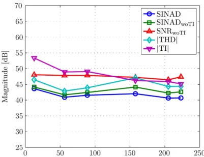
The measured SINAD, SNR, THD, and TI spurious components versus input frequency for a randomly selected die sample are shown in Fig 4. With a full-scale input tone, all metrics remain approximately flat up to the Nyquist frequency.
Fig. 4 Measured SINAD, SNR, THD, and TI spur versus fin at fs ≈ 464 MS/s and Vin ≈−0.1 dBFS
(time-interleaving spur is removed, i.e. “woTI”).
DUT with Internal Analog Input and Clock
In this case both the analog input signal and the clock signal are provided internally by means of PLLIN
and PLLCK, respectively. Thus, the complete BIST system is evaluated.
The amplitude of the sinusoidal signal generated by PLLIN directly influences the THD of the analog input signal to the ADC, because the voltage-controlled oscillator produces more distortion as the oscillation amplitude increases, and also because the linear buffer that follows the VCO and drives the track-and-hold stage of the ADC becomes more nonlinear as the input signal increases.
Since in this work the distortion of the VCO dominates and increases when the output differential amplitude of the VCO becomes larger than Vin = 600 mVpp,diff, we set the analog input amplitude to this
level. Given that the input full-scale range of the ADC is nominally 800 mVpp,diff, this level of Vin
corresponds to −2.5 dBFS. If we were not constrained by the distortion of the VCO, we would choose a larger analog input level, e.g., −0.1 dBFS (corresponding to 790 mVpp,diff in this case), in order to exercise
almost all output codes of the ADC.
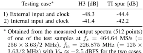
Table 3 summarizes the highest harmonic and TI tone from the measured output spectra for the evaluation cases. For a fair comparison, we use the same frequencies and amplitude for all cases. We note in case 1) that besides the fundamental tone, a set of odd harmonics, dominated by the third harmonic (−48.3 dB), and the TI spurious tone (−44.4 dB), which is the strongest in the spectrum.
In case 2), the third harmonic level is −41.4 dB and the TI spurious tones is −42.2 dB. We have a 6.9 dB difference in the third harmonic and a 2.2 dB difference in the TI spurious components level. The larger discrepancy in the third harmonic level is mainly due to the increased distortion introduced by the VCO of PLLIN (even though we are using a Vin ≈ −2.5 dBFS).
Similar conclusions can be drawn analysing the output spectra of other two randomly selected die samples.
In summary, we can say that the quality of the analog input and clock signals produced by the PLLs of the BIST scheme proposed in this work allows us to evaluate an ADC with a SFDR as high as about 41.4 dB when sampling an almost-Nyquist-frequency tone at about 500 MS/s.
Discussion
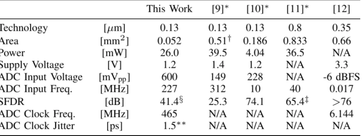
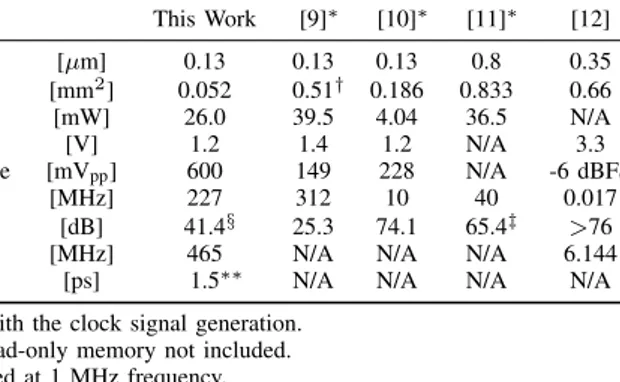
The BIST scheme proposed in this work can be compared with other works in the literature, as shown in Table 4.
One of the key requisites of a BIST circuitry is small area overhead, since the extra silicon area affects both the overall cost and yield of the ICs. As we can see in Table 4, our work has an almost fourfold area improvement compared with the most area-efficient implementation, even ignoring that the other works do not deal with the clock signal generation. This improvement is achieved by a judicious selection of circuit topologies and techniques. For instance, instead of using area-hungry LC oscillators to build up the voltage-controlled oscillators of the phase-locked loops, we use simple RC oscillators. We use a capacitance multiplication scheme to reduce the capacitances, and consequently the silicon area, of the loop filters of the PLLs.
The power dissipation of the BIST circuits is not very important because they are used only during a fraction of the operation time of the remaining (core) circuits, usually during the power-on or during idle time slots. After the self-test procedures, the BIST circuits are turned-off, dropping the power dissipated by these circuits to (almost) zero. Hence, even though the BIST circuits proposed in this work dissipate a relatively high power, 26 mW, this is acceptable for the target application.
We compare the quality of the analog input signal to the DUT using the SFDR metric. Even though the measured SFDR of this work is worse than that of [10]-[12], it is obtained for much higher analog input
frequencies and amplitudes. For example, the SFDR of 74.1 dB reported in [10] is for an analog input frequency as low as 10 MHz and for a low differential amplitude, 228 mVpp. In general, it is unfeasible or
very difficult to keep a high SFDR with high analog input frequency and/or amplitude, since the circuits suffer from higher distortions or bandwidth. This is shown in the SFDR of 25.3 dB reported in [9], where the input frequency is 312 MHz.
The main limitations of the generated analog input and clock signals of the proposed BIST scheme are the following:
• Distortion in the analog input signal. The sources of these distortions are the nonlinearity of the VCO
of PLLIN, and also the nonlinearity of the buffer that follows this VCO and drives the front-end track-and-hold of the ADC.
• Phase noise (or jitter) in the analog input and clock signals. The source of this noise is mainly the
noise in the active devices of the VCOs in PLLIN and PLLCK.
• Deterministic reference spurious tones, which are nonidealities (mainly mismatches) in the charge
pumps of both PLLCK and PLLIN.
These limitations can be minimized by improving the sizing of the circuits, by enhancements in the circuit topologies, and by careful layouts. Also, some of these limitations are more severe than others. For example, the deterministic reference spurs are not problematic, since they can be easily separated from the actual performance of the ADC under test. In this work, we achieve a worst-case (for three measured samples) SFDR as high as 41.4 dB for an analog input frequency of about 227 MHz with differential amplitude of 600 mVpp. The SFDR of the generated analog input signal is also dependent on the supply
voltage, since reducing this (which is the trend for newer CMOS technologies) equally reduces the voltage headroom available to keep the active devices operating in saturation. In other words, reducing the supply voltage increases the distortion of a given circuit topology, maintaining the same signal swing, unless topology changes (if viable) are made.
The phase noise (or jitter) present in both the output of two PLLs were not measured due to reduced number of I/O pins. By post-layout simulations, we can estimate the integrated rms jitter (above 1 MHz offset) of PLLCK as 1.5 ps, as indicated in Table 4. This result, however, cannot be compared with those of other works, since these works only address the analog input signal generation.
Table 4 – Performance summary and comparison with prior works.
CONCLUSIONS
In this paper we present an overview of challenges in testing ADCs at high frequencies, which will be a hot topic in near future, due to the continuous advances of CMOS technologies. We review the advantages and disadvantages of BIST approaches and show that BIST can be a promising solution for functional and dynamic testing of high speed ADCs.
We present a fully integrated BIST technique, together with experimental results, targeting high-frequency and moderate resolution ADCs. This fully integrated, low cost, and reconfigurable architecture for coherent self-testing of high speed ADCs is based on two synchronized PLLs, one to synthesize the analog input signal and another to synthesize the clock signal for the ADC under test. This synchronization is a key feature of the proposed approach, since it allows coherent sampling. With coherent sampling, the digital output data of the converter are well-behaved and their spectrum is unambiguous, since it is not necessary to worry with spectral leakage, windowing, etc. Hence, with a reduced record length and a relatively low-complexity DSP hardware, it is feasible to do a reliable spectral analysis to assess the dynamic performance of the ADC.
Even though the proof-of-concept is made with a moderate resolution converter, the method proposed can be extended to low- and high-resolution ADCs. The proposed BIST architecture for ADCs is reconfigurable: it is possible to synthesize different analog input and clock frequencies by simply changing
the frequency dividers values related to the PLLs. The frequency ranges depend on the locking ranges of the PLLs. The complete BIST system has been implemented in a 0.13 µm CMOS technology and experimentally evaluated to validate the proposed method.
REFERENCES
[1] P. Daponte, L. D. Vito, S. Rapuano and I. Tudosa, "Analog-to-information converters in the wideband rf measurement for aerospace applications: current situation and perspectives," in IEEE Instrumentation & Measurement Magazine, vol. 20, no. 1, pp. 20-28, February 2017.
[2] J. Blair, “Histogram measurement of ADC nonlinearities using sine waves,” IEEE Trans. Instrum. Meas., vol. 43, pp. 373– 383, Mar. 1994.
[3] J. Blair, “Selecting test frequencies for sinewave tests of ADCs,” in Proc. IEEE Instrumentation and Measurement
Technology Conference (IMTC’02), 2002, pp. 189–193.
[4] T. Sundstrom, C. Svensson, and A. Alvandpour, “A 2.4 GS/s, singlechannel, 31.3 dB SNDR at Nyquist, pipeline ADC in 65 nm CMOS,” IEEE J. Solid-State Circuits, vol. 46, pp. 1575–1584, Jul. 2011.
[5] M. L. Bushnell and V. D. Agrawal, Essentials of Electronic Testing for Digital, Memory and Mixed-Signal VLSI Circuits. New York: Kluwer Academic Publishers, 2002.
[6] Future Fab International, Special Focus: International Technology Roadmap for Semiconductors, vol. 36, Jan. 2011. [7] E. Santin, L. B. Oliveira, B. Nowacki, and J. Goes, “A fully integrated and reconfigurable architecture for coherent
self-testing of high speed analog-to-digital converters,” IEEE Trans. Circuits Syst. I, vol. 58, pp. 1531–1541, Jul. 2011.
[8] E. Santin, “A Built-In Self-Test Technique for High Speed Analog-to-Digital Converters,” Ph.D. dissertation, Universidade Nova de Lisboa, Lisbon, 2014. Accessed on: August 5, 2019. [Online]. Available: http://hdl.handle.net/10362/14389 [9] J. Wibbenmeyer and C.-I. H. Chen, “Built-in self-test for low-voltage high-speed analog-to-digital converters,” IEEE
Trans. Instrum. Meas., vol. 56, pp. 2748–2756, Dec. 2007.
[10] M. M. Elsayed and E. Sanchez-Sinencio, “A low THD, low power, high´ output-swing time-mode-based tunable oscillator via digital harmoniccancellation technique,” IEEE J. Solid-State Circuits, vol. 45, pp. 1061– 1071, May 2010.
[11] B. Dufort and G. W. Roberts, “On-chip analog signal generation for mixed-signal built-in self-test,” IEEE J. Solid-State
Circuits, vol. 34, pp.
318–330, Mar. 1999.
[12] H. C. Hong, F. Y. Su, and S. F. Hung, “A fully integrated built-in self-test ADC based on the modified controlled sine-wave fitting procedure,” IEEE Transactions on Instrumentation and Measurement, vol. 59, no. 9, pp. 2334–2344, Sept 2010.
Edinei Santin (S’07-M’15) was born in Marau, Brazil, in 1986. He received the BSc degree in Electrical Engineering from
Federal University of Santa Maria, Santa Maria, Brazil, in 2008, and the PhD degree in Electrical and Computer Engineering from Universidade Nova de Lisboa, Lisbon, Portugal, in 2014. From March 2015 to February 2018 he was a Senior Fellow at the European Organization for Nuclear Research, Geneva, Switzerland, working on the design of hybrid and monolithic silicon pixel detectors for medical imaging and future particle colliders. His research interests include analog and mixed-signal integrated circuits, data converters, monolithic and hybrid silicon pixel detectors, and built-in self-testing and self-calibration techniques.
Luis B. Oliveira was born in Lisbon, Portugal, in 1979. He graduated with a degree in electrical and computer engineering, and
a Ph.D. degree, in 2002 and 2007 respectively, from Instituto Superior Técnico (IST), Technical University of Lisbon. In 2007, he joined the teaching staff of the Department of Electrical Engineering of Faculdade de Ciências e Tecnologia, Universidade Nova de Lisboa, and is currently a researcher at CTS-UNINOVA.
Prof. Oliveira is an IEEE Senior Member, vice-chair of the IEEE Portugal Executive Committee, for the period 2018-2019, and chair of the Broadcast Technology Society, Circuits and Systems Society, and Consumer Electronics Society, IEEE Joint Chapter, since 2016. He is a member of the IEEE CASS Analog Signal Processing Technical Committee, ASPTC, (the largest within CASS), since 2008. He has more than 100 publications in International Journals and Conferences, and is co-author of two books: “Analysis and Design of Quadrature Oscillators” (Springer, 2008) and “Wideband CMOS Receivers”, (Springer, 2015). He is currently an Associate Editor of the IEEE Transactions on Circuits and Systems – II, TCAS-II, for the term 2018-2019.
Joao Goes received the B.Sc., M.Sc., and Ph.D. degrees in electrical and computer engineering from Instituto Superior Tecnico
(IST), Technical University of Lisbon, Lisbon, Portugal, in 1992, 1996, and 2000, respectively, and the Agregado degree (Habilitation degree) in electronics from the Universidade Nova de Lisboa (UNL), Caparica, Portugal, in 2012. Since April 1998, he has been with the Department of Electrical Engineering (DEE), Faculdade de Cincias e Tecnologia (FCT), UNL,
where he is currently a Full Professor and has been the Department Head since July 2012. Since 1998, he has been a Senior Researcher, responsible for the Micro/Nanoelectronics Research Unit, with the Centre of Technology and Systems (CTS), Instituto de Desenvolvimento de Novas Tecnologias (UNINOVA). In November 2012, he also became the Director of CTS. Since 1992, he has participated and led several national and European projects in science, technology, and training. He has also supervised (graduated) 12 Ph.D. theses, 24 M.Sc. theses, and nine graduation projects. He has published over 180 papers in international journals and leading IEEE conferences. He was the TPC Co- Chairman of IEEE ISCAS 2015 held in Lisbon on May, 2015 and the TPC Co-Chairman of PRIME 2016. He is currently an Associate Editor of the IEEE TRANSACTIONS ON CIRCUITS AND SYSTEMSII for the period 2016-2019.
Advantages Disadvantages vertical testability (wafer to system) area overhead
high diagnosis resolution performance penalties full-speed testing additional design time & effort reduced need for external test equipment additional risk to project
reduced test development time & effort difficulty to reach full accuracy reduced manufacturing test time & effort
reduced time-to-market
complete BIST system has been implemented in a 0.13 µm
CMOS tecnhology and experimentaly evaluated to validate the proposed method.
REFERENCES
[1] J. Blair, “Histogram measurement of ADC nonlinearities using sine waves,” IEEE Trans. Instrum. Meas., vol. 43, pp. 373–383, Mar. 1994. [2] J. J. Blair, “Selecting test frequencies for sinewave tests of ADCs,” in Proc. IEEE Instrumentation and Measurement Technology Conference (IMTC’02), 2002, pp. 189–193.
[3] T. Sundstrom, C. Svensson, and A. Alvandpour, “A 2.4 GS/s, single-channel, 31.3 dB SNDR at Nyquist, pipeline ADC in 65 nm CMOS,” IEEE J. Solid-State Circuits, vol. 46, pp. 1575–1584, Jul. 2011. [4] K. Poulton et al., “A 20GS/s 8b ADC with a 1MB memory in 0.18µm
CMOS,” in Proc. IEEE International Solid-State Circuits Conference (ISSCC’03), 2003, pp. 318–496.
[5] P. Schvan et al., “A 24GS/s 6b ADC in 90nm CMOS,” in Proc. IEEE International Solid-State Circuits Conference (ISSCC’08), Feb. 2008, pp. 544–634.
[6] Y. Ke, J. Craninckx, and G. Gielen, “A design approach for power-optimized fully reconfigurable ∆Σ A/D converter for 4G radios,” IEEE Trans. Circuits Syst. II, vol. 55, pp. 229–233, Mar. 2008.
[7] M. L. Bushnell and V. D. Agrawal, Essentials of Electronic Testing for Digital, Memory and Mixed-Signal VLSI Circuits. New York: Kluwer Academic Publishers, 2002.
[8] M. Burns and G. W. Roberts, An Introduction to Mixed-Signal IC Test and Measurement. New York: Oxford University Press, 2001. [9] E. Santin, L. B. Oliveira, B. Nowacki, and J. Goes, “A fully integrated
and reconfigurable architecture for coherent self-testing of high speed analog-to-digital converters,” IEEE Trans. Circuits Syst. I, vol. 58, pp. 1531–1541, Jul. 2011.
[10] F. M. Gardner, “Charge-pump phase-lock loops,” IEEE Trans. Commun., vol. COM-28, pp. 1849–1858, Nov. 1980.
[11] B. Razavi, Ed., Phase-Locking in High Performance Systems: From Devices to Architectures. Hoboken, NJ: Wiley-IEEE Press, 2003. [12] L. B. Oliveira, J. R. Fernandes, I. M. Filanovsky, C. J. M. Verhoeven, and
M. M. Silva, Analysis and Design of Quadrature Oscillators. Dordrecht: Springer, 2008.
[13] A. Kral, F. Behbahani, and A. A. Abidi, “RF-CMOS oscillators with switched tuning,” in Proc. IEEE Custom Integrated Circuits Conference (CICC’98), 1998, pp. 555–558.
[14] E. Hegazi, H. Sjoland, and A. A. Abidi, “A filtering technique to lower LC oscillator phase noise,” IEEE J. Solid-State Circuits, vol. 36, pp. 1921–1930, Dec. 2001.
[15] I. G. Finvers and I. M. Filanovsky, “Analysis of a source-coupled CMOS multivibrator,” IEEE Trans. Circuits Syst., vol. 35, pp. 1182–1185, Sep. 1988.
[16] V. von Kaenel, D. Aebischer, C. Piguet, and E. Dijkstra, “A 320 MHz, 1.5 mW @ 1.35 V CMOS PLL for microprocessor clock generation,” IEEE J. Solid-State Circuits, vol. 31, pp. 1715–1722, Nov. 1996. [17] K. R. Lakshmikumar, “Analog PLL design with ring oscillators at
low-gigahertz frequencies in nanometer CMOS: Challenges and solutions,” IEEE Trans. Circuits Syst. II, vol. 56, pp. 389–393, May 2009. [18] T.-H. Lin and W. J. Kaiser, “A 900-MHz 2.5-mA CMOS frequency
synthesizer with an automatic SC tuning loop,” IEEE J. Solid-State Circuits, vol. 36, pp. 424–431, Mar. 2001.
[19] C. S. Vaucher, I. Ferencic, M. Locher, S. Sedvallson, U. Voegeli, and Z. Wang, “A family of low-power truly modular programmable dividers in standard 0.35-µm CMOS technology,” IEEE J. Solid-State Circuits, vol. 35, pp. 1039–1045, Jul. 2000.
[20] J. Wibbenmeyer and C.-I. H. Chen, “Built-in self-test for low-voltage high-speed analog-to-digital converters,” IEEE Trans. Instrum. Meas., vol. 56, pp. 2748–2756, Dec. 2007.
[21] M. M. Elsayed and E. S´anchez-Sinencio, “A low THD, low power, high output-swing time-mode-based tunable oscillator via digital harmonic-cancellation technique,” IEEE J. Solid-State Circuits, vol. 45, pp. 1061– 1071, May 2010.
[22] B. Dufort and G. W. Roberts, “On-chip analog signal generation for mixed-signal built-in self-test,” IEEE J. Solid-State Circuits, vol. 34, pp. 318–330, Mar. 1999.
[23] H. C. Hong, F. Y. Su, and S. F. Hung, “A fully integrated built-in self-test Σ−∆ ADC based on the modified controlled sine-wave fitting procedure,” IEEE Transactions on Instrumentation and Measurement, vol. 59, no. 9, pp. 2334–2344, Sept 2010.
TABLE I
PROGRAMMABLE PARAMETERS AND FREQUENCY MAP FOR A6-BITADC (ALL FREQUENCIES ARE EITHER INMHZ ORMS/S). fref≡ 4 MHz fˆs1≡ 250 fˆs2≡ 500 fˆs3≡ 1000 N ≡ 6 bits Ns= 256 Mf 1= 4 M2= 2 M3= 1 s1= 256 fs2= 512 fs3= 1024 ˆ fin1/fs≡ 1/2 Np1= 127 fin11= 127 fin12= 254 fin13= 508 ˆ fin2/fs≡ 1/4 Np2= 63 fin21= 63 fin22= 126 fin23= 252 ˆ fin3/fs≡ 1/8 Np3= 31 fin31= 31 fin32= 62 fin33= 124 TABLE II
PROGRAMMABLE PARAMETERS AND FREQUENCY MAP FOR A6-BITADC (ALL FREQUENCIES ARE EITHER INMHZ ORMS/S).
fref≡ 4 MHz fˆs1 ≡ 250 fˆs2≡ 500 fˆs3≡ 1000 N ≡ 6 bits Ns= 256 Mf 1= 4 M2= 2 M3= 1 s1 = 256 fs2= 512 fs3= 1024 ˆ fin1/fs≡ 1/2 Np1= 127 fin11 = 127 fin12 = 254 fin13= 508 ˆ fin2/fs≡ 1/4 Np2= 63 fin21 = 63 fin22 = 126 fin23= 252 ˆ fin3/fs≡ 1/8 Np3= 31 fin31 = 31 fin32 = 62 fin33= 124
∗All frequencies are in MHz or MS/s.
PFD Main/Aux.CPs BPM CP V VBPACP LF Two-integratorVCO BPR RB V 0 vcoi nb ampl ctrl (from pad) Linear buffer BPLI NB V DIFF/SE converter vipbist vinbist BPD IFFS E V FD i p N ÷ pin pin 0,..., 6 7 pllin iref PLL IN GBC BPM CP V BPAC P V BPRR B V BPLI NB V BPDI FFS E V pllinvdda/vssa bypass 837pF ∼ vrefpfd / pllinvdda vssa / pllinvddd vssd pllinvddd/vssd bypass 206pF ∼
Fig. 3. Block diagram of the PLLIN.
divider Npi must have values of at least Np1,2 ={63, 127} in order to generate the intended frequency ranges. As a consequence, the frequency divider of PLLIN is programmable by means of the control bitspin0, pin1, . . . , pin6, shown in Fig. 3 and addressed later, allowing integer frequency division from 32 to 127.
In order to accommodate the two frequency ranges (i.e., around 250 and 500 MHz) without relying on considerable different VCO gains, the two-integrator VCO employs two discrete tuning characteristics, one for each frequency range. The selection between one discrete tuning curve or another is
done through vcoinb0, which comes from the configuration
logic block.
The amplitude of sinusoidal signals generated by the
two-integrator VCO can be adjusted by means of the amplctrl
signal, which is set through an external pin.
Another external pin, plliniref, is used to provide an on-chip independent reference current to PLLIN. This reference cur-rent is then mirrored by a global biasing circuit and distributed to the circuits of the PLLIN. This approach is important to distribute biasing signals separated by large distances in current domain instead of in the voltage domain (the latter
PFD Main/Aux.CPs BPM CP V VBPACP LF RelaxationVCO BPR RB V 0 vcoc kb ckbist FD s N ÷ pllckir ef PLL CK GBC BPM CP V BPA CP V BPR RB V BPD IFFS E V pllckvdda/vssa bypass 829pF ∼ vrefpfd / pllckvdda vssa / pllckvddd vssd pllckvddd/vssd bypass 245pF ∼ DIFF/SE converter BPD IFFSE V
Fig. 4. Block diagram of the PLLCK.
susceptible to IR drops and other sources of error).
Two separated power/ground domains (analog and digital) are used for PLLIN, as shown in Fig. 3. The digital domain is more noisy and it powers the DIFF/SE converter and the frequency divider, which operate at the maximum frequency of the PLL and, as a result, produce significant transient current impulses into the respective power/ground lines.
B. PLLCK Overview
The clock PLL is also based on an integer-N charge pump topology, as shown in Fig. 4. However, differently from the analog input PLL, it resembles a more conventional PLL used for ubiquitous clock generation.
The main function of PLLCK is to generate a low jitter and high frequency clock signal (ckbist) based on a relatively low frequency signal (vrefpfd), which is also shared with PLLIN. The sharing of vrefpfd allows both PLLs be synchronized when they acquire lock state (i.e., enter steady state regime). This in turn enables the DUT to sample the analog input signal in a coherent fashion. Moreover, it is interesting to note that any phase noise on vrefpfd within the loop bandwidth of the
TABLE III H3ANDTISPUR
Testing case∗ H3 [dB] TI spur [dB] 1) External input
and clock -48.3 -44.4
2) External input and
internal clock -51.7 -46.4 3) Internal input
and clock -41.4 -42.2
∗Obtained from the measured output spectra (512
points) of Sample 1 at fs = 464.64 MS/s (=
256 × 3.63/2 MHz), fin = 226.875 MHz (=
125 × 3.63/2 MHz) with Vin≈ −2.5 dBFS for
the three cases.
TABLE IV
PERFORMANCE SUMMARY AND COMPARISON WITH PRIOR WORKS. This Work [20]∗ [21]∗ [22]∗ [23]
Technology [µm] 0.13 0.13 0.13 0.8 0.35
Area [mm2] 0.052 0.51† 0.186 0.833 0.66
Power [mW] 26.0 39.5 4.04 36.5 N/A
Supply Voltage [V] 1.2 1.4 1.2 N/A 3.3
ADC Input Voltage [mVpp] 600 149 228 N/A -6 dBFS
ADC Input Freq. [MHz] 227 312 10 40 0.017
SFDR [dB] 41.4§ 25.3 74.1 65.4‡ >76
ADC Clock Freq. [MHz] 465 N/A N/A N/A 6.144
ADC Clock Jitter [ps] 1.5∗∗ N/A N/A N/A N/A
∗Do not deal with the clock signal generation. †Area of the read-only memory not included. ‡SFDR measured at 1 MHz frequency. §Ignoring PLLs reference spurs.
∗∗Jitter rms integrated above 1 MHz and estimated from simulation.
TABLE V H3ANDTISPUR
Testing case∗ H3 [dB] TI spur [dB] 1) External input and clock -48.3 -44.4 2) Internal input and clock -41.4 -42.2
∗Obtained from the measured output spectra (512 points)
of one of the test samples at fs = 464.64 MS/s (=
256 × 3.63/2 MHz), fin= 226.875 MHz (= 125 ×
3.63/2 MHz) with Vin≈ −2.5 dBFS for the two cases.
experimental results, targeting high-frequency and moderate resolution ADCs.
V. CONCLUSION
A fully integrated, low cost, and reconfigurable architecture for coherent self-testing of high speed ADCs is presented in this work. The proposed built-in self-test solution is based on two synchronized PLLs, one to synthesize the analog input signal and another to synthesize the clock signal for the ADC under test. This synchronization is a key feature of the proposed approach, since it allows coherent sampling.
With coherent sampling, the digital output data of the converter are well-behaved and their spectrum is unambiguous, since it is not necessary to worry with spectral leakage, windowing, etc. Hence, with a reduced record length and a relatively low-complexity DSP hardware, it is feasible to do a reliable spectral analysis to assess the dynamic performance of the ADC.
Special techniques and circuits were adopted to implement compact and dedicated PLLs for this particular application. These techniques allowed to reduce the area of the BIST circuitry considerably while producing good analog input and clock signals, in terms of phase noise and distortion. Even though the proof-of-concept is made with a moderate resolu-tion converter, the method proposed can be extended to low and high resolution ADCs. The proposed BIST architecture for ADCs is reconfigurable: it is possible to synthesize different analog input and clock frequencies by simply changing the frequency dividers values related to the PLLs. The frequency ranges depend on the locking ranges of the PLLs. The
complete BIST system has been implemented in a0.13 µm
CMOS tecnhology and experimentaly evaluated to validate the proposed method.
REFERENCES
[1] J. Blair, “Histogram measurement of ADC nonlinearities using sine waves,” IEEE Trans. Instrum. Meas., vol. 43, pp. 373–383, Mar. 1994. [2] J. J. Blair, “Selecting test frequencies for sinewave tests of ADCs,” in Proc. IEEE Instrumentation and Measurement Technology Conference (IMTC’02), 2002, pp. 189–193.
[3] T. Sundstrom, C. Svensson, and A. Alvandpour, “A 2.4 GS/s, single-channel, 31.3 dB SNDR at Nyquist, pipeline ADC in 65 nm CMOS,” IEEE J. Solid-State Circuits, vol. 46, pp. 1575–1584, Jul. 2011. [4] K. Poulton et al., “A 20GS/s 8b ADC with a 1MB memory in 0.18µm
CMOS,” in Proc. IEEE International Solid-State Circuits Conference (ISSCC’03), 2003, pp. 318–496.
[5] P. Schvan et al., “A 24GS/s 6b ADC in 90nm CMOS,” in Proc. IEEE International Solid-State Circuits Conference (ISSCC’08), Feb. 2008, pp. 544–634.
[6] Y. Ke, J. Craninckx, and G. Gielen, “A design approach for power-optimized fully reconfigurable ∆Σ A/D converter for 4G radios,” IEEE Trans. Circuits Syst. II, vol. 55, pp. 229–233, Mar. 2008.
[7] M. L. Bushnell and V. D. Agrawal, Essentials of Electronic Testing for Digital, Memory and Mixed-Signal VLSI Circuits. New York: Kluwer Academic Publishers, 2002.
[8] M. Burns and G. W. Roberts, An Introduction to Mixed-Signal IC Test and Measurement. New York: Oxford University Press, 2001. [9] E. Santin, L. B. Oliveira, B. Nowacki, and J. Goes, “A fully integrated
and reconfigurable architecture for coherent self-testing of high speed analog-to-digital converters,” IEEE Trans. Circuits Syst. I, vol. 58, pp. 1531–1541, Jul. 2011.
[10] F. M. Gardner, “Charge-pump phase-lock loops,” IEEE Trans. Commun., vol. COM-28, pp. 1849–1858, Nov. 1980.
[11] B. Razavi, Ed., Phase-Locking in High Performance Systems: From Devices to Architectures. Hoboken, NJ: Wiley-IEEE Press, 2003. [12] L. B. Oliveira, J. R. Fernandes, I. M. Filanovsky, C. J. M. Verhoeven, and
M. M. Silva, Analysis and Design of Quadrature Oscillators. Dordrecht: Springer, 2008.
[13] A. Kral, F. Behbahani, and A. A. Abidi, “RF-CMOS oscillators with switched tuning,” in Proc. IEEE Custom Integrated Circuits Conference (CICC’98), 1998, pp. 555–558.
TABLE III H3ANDTISPUR
Testing case∗ H3 [dB] TI spur [dB] 1) External input
and clock -48.3 -44.4
2) External input and
internal clock -51.7 -46.4 3) Internal input
and clock -41.4 -42.2
∗Obtained from the measured output spectra (512
points) of Sample 1 at fs = 464.64 MS/s (=
256 × 3.63/2 MHz), fin = 226.875 MHz (=
125 × 3.63/2 MHz) with Vin≈ −2.5 dBFS for
the three cases.
TABLE IV
PERFORMANCE SUMMARY AND COMPARISON WITH PRIOR WORKS. This Work [20]∗ [21]∗ [22]∗ [23]
Technology [µm] 0.13 0.13 0.13 0.8 0.35
Area [mm2] 0.052 0.51† 0.186 0.833 0.66
Power [mW] 26.0 39.5 4.04 36.5 N/A
Supply Voltage [V] 1.2 1.4 1.2 N/A 3.3
ADC Input Voltage [mVpp] 600 149 228 N/A -6 dBFS
ADC Input Freq. [MHz] 227 312 10 40 0.017
SFDR [dB] 41.4§ 25.3 74.1 65.4‡ >76
ADC Clock Freq. [MHz] 465 N/A N/A N/A 6.144
ADC Clock Jitter [ps] 1.5∗∗ N/A N/A N/A N/A
∗Do not deal with the clock signal generation. †Area of the read-only memory not included. ‡SFDR measured at 1 MHz frequency. §Ignoring PLLs reference spurs.
∗∗Jitter rms integrated above 1 MHz and estimated from simulation.
TABLE V H3ANDTISPUR
Testing case∗ H3 [dB] TI spur [dB] 1) External input and clock -48.3 -44.4
2) Internal input and clock -41.4 -42.2
∗Obtained from the measured output spectra (512 points)
of one of the test samples at fs = 464.64 MS/s (=
256 × 3.63/2 MHz), fin= 226.875 MHz (= 125 ×
3.63/2 MHz) with Vin≈ −2.5 dBFS for the two cases.
TABLE VI
PERFORMANCE SUMMARY AND COMPARISON WITH PRIOR WORKS. This Work [9]∗ [10]∗ [11]∗ [12]
Technology [µm] 0.13 0.13 0.13 0.8 0.35
Area [mm2] 0.052 0.51† 0.186 0.833 0.66
Power [mW] 26.0 39.5 4.04 36.5 N/A
Supply Voltage [V] 1.2 1.4 1.2 N/A 3.3
ADC Input Voltage [mVpp] 600 149 228 N/A -6 dBFS
ADC Input Freq. [MHz] 227 312 10 40 0.017
SFDR [dB] 41.4§ 25.3 74.1 65.4‡ >76
ADC Clock Freq. [MHz] 465 N/A N/A N/A 6.144
ADC Clock Jitter [ps] 1.5∗∗ N/A N/A N/A N/A
∗Do not deal with the clock signal generation. †Area of the read-only memory not included. ‡SFDR measured at 1 MHz frequency. §Ignoring PLLs reference spurs.
∗∗Jitter rms integrated above 1 MHz and estimated from simulation.
experimental results, targeting high-frequency and moderate resolution ADCs.
V. CONCLUSION
A fully integrated, low cost, and reconfigurable architecture for coherent self-testing of high speed ADCs is presented in this work. The proposed built-in self-test solution is based on two synchronized PLLs, one to synthesize the analog input signal and another to synthesize the clock signal for the ADC under test. This synchronization is a key feature of the proposed approach, since it allows coherent sampling.
With coherent sampling, the digital output data of the converter are well-behaved and their spectrum is unambiguous, since it is not necessary to worry with spectral leakage, windowing, etc. Hence, with a reduced record length and a
relatively low-complexity DSP hardware, it is feasible to do a reliable spectral analysis to assess the dynamic performance of the ADC.
Special techniques and circuits were adopted to implement compact and dedicated PLLs for this particular application. These techniques allowed to reduce the area of the BIST circuitry considerably while producing good analog input and clock signals, in terms of phase noise and distortion. Even though the proof-of-concept is made with a moderate resolu-tion converter, the method proposed can be extended to low and high resolution ADCs. The proposed BIST architecture for ADCs is reconfigurable: it is possible to synthesize different analog input and clock frequencies by simply changing the frequency dividers values related to the PLLs. The frequency ranges depend on the locking ranges of the PLLs. The