A Voltage Controlled Oscillator Using IGZO
Thin-Film Transistors
Tejaswini Keragodu
a, Bhawna Tiwari
a, Nishtha
a, Pydi Bahubalindruni
a, Joao Goes
b, Pedro Barquinha
c,
a IIIT-Delhi, Okhla Industrial Estate, Phase III, New Delhi, India - 110020b Department of Electrical Engineering, Universidade NOVA de Lisboa, CTS-UNINOVA, Campus de Caparica, 2829-516, Portugal c i3N/CENIMAT, Department of Materials Science and Technology,
Universidade NOVA de Lisboa and CEMOP-UNINOVA, Campus de Caparica, 2829-516 Caparica, Portugal
Abstract—This paper presents a voltage controlled oscillator (VCO) using amorphous Indium Gallium Zinc Oxide (a-IGZO) thin-film transistors (TFTs). This circuit consists of a high-gain OpAmp, a comparator and a relaxation oscillator. The implemented relaxation oscillator shows a power consumption of 700 µW, when it is simulated with a supply rails of ±5 V. It shows a frequency of oscillation range from 327 to 560 Hz, when the tuning capacitance value is in varying from 1.6 to 5 pF. On the other hand, the VCO has a power dissipation of 1.3 mW with frequency ranging from 400 to 556 Hz with a controlling voltage from -5 to 5 V. In-house oxide TFT model is used for circuit simulations in Cadence environment. This circuit would find potential applications in large-area flexible systems, namely smart packaging, biomedical and wearable systems, which needs clocks with different frequencies.
Keywords—Relaxation Oscillator, a-IGZO TFTs, comparator with oxide TFTs, positive feedback operational amplifier.
I. INTRODUCTION
Amorphous Indium Gallium Zinc Oxide (a-IGZO) thin-film transistors (TFTs) are gaining significant interest in various real-world applications including smart packaging, biomedical and wearable systems due to their low-temperature fabrication [1], relative high mobility (>10cm2/V.s) and the stability compared to the other competing low-temperature TFT technologies (a-Si:H and organic TFTs). However, these technologies impose challenges in circuit design due to the absence of a stable complementary device.
In order to ensure compact flexible systems, all the circuits need to be on-chip to eliminate external interface problems. On-chip clock generator is one of the important functional block with frequency of oscillation tuning ability. Though many ring oscillators were reported with IGZO TFTs, they have the limitation of inferior swing, very high supply voltages (≥ 15 V) and a single frequency of oscillation [2], [3], [4], [5]. Nevertheless, a ring oscillator with almost full swing is reported with bootstrapping load, this circuit is also limited to a single frequency of oscillation [6].
In order to address the above mentioned challenges, this work proposes a voltage controlled oscillator (VCO) using IGZO TFTs that contains an OpAmp, a comparator and a relaxation oscillator. Since there is an absence of stable and reproducible p-type oxide TFT, CMOS design techniques cannot be adapted directly, and all desired circuit blocks are
to be designed only with n-type transistors. As a first step, an OpAmp and a comparator are designed and characterized. Then the relaxation oscillator and VCO are implemented and simulated using an in-house oxide TFT model [7] in Cadence environment. It should be noted that the model is capable of predicting the circuit behavior very close to the measured response, when the circuit is fabricated under same conditions as the TFTs, whose data was used for model development [7]. The rest of the paper is organised as follows. Section II demonstrates the proposed circuit design and its operating principle. Section III presents the simulation results and dis-cussions and finally the conclusions are drawn in section IV.
II. CIRCUITDESCRIPTION
The VCO has been implemented as shown in Fig.1. It is comprised of a relaxation oscillator, which is implemented with comparator and an OpAmp. The design of all these circuits with only n-type oxide TFTs are explained as follows.
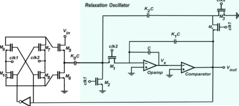
clk1 clk2 M4 M3 K1 K2C C C Vx Comparator Opamp K0C clk2 clk1 Vin M1 M2 M5 M6 M7 M8 M9 M10 Vout clk2 clk1
Fig. 1. Circuit diagram of voltage controlled oscillator.
Operational Amplifier: It is an important functional block in the relaxation oscillator circuit and it plays a vital role in minimizing stringent requirements of the comparator design presented in Fig. 1. Circuit schematic of the OpAmp is shown in Fig. 2, where the differential pair formed by transistors M1
-M4 form a positive feedback loop. The loop gain is Af as
shown in (1). It can be observed that this gain depends on aspect ratios of the transistors forming positive feedback. The aspect ratios of transistors are carefully selected to get the loop gain close to unity. When Af ≥ 1, the OpAmp can become
single ended converter, which is followed by a common-drain stage. M13 M4 M2 M11 M15 M3 M1 M12 Vout VDD VSS VSS VSS Vbias1 Vbias2 V in-Vin+ M8 M9 M6 M7 M16 M14 M5 M10
Fig. 2. Circuit diagram of operational amplifier with positive feedback
|Af| = gm7( 1 gm9||ro7||ro9 ) =gm7 gm9 (1)
The gain of the differential to single ended conversion stage is given by,
AS = gm11(
1 gm11||ro14||ro11
) (2)
and the overall gain of the Opamp is given by, Av= gm1( 1 gm9(1 − Af)||ro1||ro3 )gm11( 1 gm11||ro11||ro14 ) ≈ gm1ro1||ro3 (3)
Comparator: The architecture of the proposed comparator is shown in Fig.3. In order to ensure faster response, and get rid of clock feed-through and kickback noise, the proposed comparator consists of three preamplification stages and a static latch. Each preamplifier consists of a differential pair with positive feedback as shown in Fig.3a. This stage can ensure high-gain due to the positive feedback even with only n-type transistors, as explained in OpAmp design. A cascade of three such stages relax comparator and latch requirements. A regenerative latch together with preamplification stages can ensure faster response.
A latch is a positive feedback regenerative circuit with cross coupled TFTs as shown in Fig.3b. Its output is a growing exponential function of the differential input as per (4). The outputs of the third preamplification stage are applied as input to the latch. Based on the relative magnitude of these signals and threshold voltage of M11and M12, proper digital rails will
be resulted at the output of the latch.
Vd(t) = Vd(0).et(gm13−
1
R11)(C111 ) (4)
where Vd(t) is the difference between Vin− and Vin+ of
Fig.3b at time t, Vd(0) is initial difference voltage, gm13 is
transconductance of M13and R11and C11are total resistance
and capacitance seen at input of M11.
Relaxation Oscillator: The relaxation oscillator circuit schematic is presented in Fig. 1, which has capacitors K1C,
K2C and C along with switches, OpAmp and comparator. The
switches are controlled by non-overlapping clocks, clk1 and clk2. To understand the working of the oscillator, assume Vout
is at VSS. A charge of K2CVSS is stored in capacitor K2C
when clk1 is high. This charge is transferred to capacitor C when clk1 is low and clk2 is high. This makes Vxnegative by
K2VSS. If this charge is sufficient enough to drive Vx below
zero then the Vout is driven to VDD. In the next on-time of
clk1, the charge stored on capacitor K2C is K2C (VSS+ VDD)
makes the charge more positive and thus Vx becomes more
negative. In the following cycles, the voltage at Vx keeps on
charging to zero in the steps of K2VDD. The frequency of
Vout is given by (5). f =K2 K1 fclk 2 + VSS VDD + VDD VSS (5) where fclk is clock frequency of switching.
Voltage Controlled Oscillator: The relaxation oscillator was used to obtain a VCO as shown in Fig.1. The capacitor K0C,
a feed-in capacitor is controlled in such way that the positive Vinadds the charge to C with the same sign of K2C making
Vxreach zero earlier, thus increasing the frequency. With Vin
the charge added to C has opposite polarity comapared to that of K2C making Vxreach zero later leading to lower frequency.
The frequency of VCO is calculated using (6). f = (K2 4K1 )fclk+ Vin( K0 4K1VDD )fclk (6)
where Vinis voltage that contorls the oscillation of the circuit.
III. RESULTS ANDDISCUSSION
Using inhouse oxide TFT model the OpAmp, the Com-parator, the Relaxation Oscillator and the Voltage Controlled Oscillator have been designed and simulated in Cadence envi-ronment with a power supply rails of ±5 V.
The performance of the OpAmp: When the positive feedback operational amplifier shown in Fig. 2 is simulated, it is showing a gain of 61.7 dB. It is stable with a phase margin of 720, power consumption of 200 µW and has a unity gain
bandwdith of 158 kHz as shown in Fig.4.
The performance of the Comparator: As stated before, the comparator in the work has three preamp stgaes and a latch as shown in Fig. 3. Whereas, Fig.5 shows the gain and phase response of a single-stage preamplifier with a gain of 10 dB and phase margin of 68o. Fig.6 shows the output response of comparator having a swing of 4.32 to -4.21. Other performance metrics of the comparator are shown in Table I.
The performance of Relaxation Oscillator: The output Vout and the intermediate voltage level Vx has been shown
M12 VDD VSS a) b) Vin- VIn+ V Out-M11 M13 M14 c} c
c Preamp1 Preamp2 Preamp3
V in-VIn+ VSS VSS VDD VIn+ V Out-VOut+ VOut+ M1 M2 M3 M4 M5 M10 M7 M8 M6 M9 Vbias1 Vbias2 V in-c) Vop+
Vop-Fig. 3. Circuit diagram of a comparator: a) Preamplifier b) Latch c) Complete Comparator
Fig. 4. Response of operational amplifier showing gain and phase plots
Fig. 5. Response of single stage preamplifier showing gain and phase plots
Fig. 6. Output of comparator showing input and output voltages TABLE I. CALCULATEDPARAMETERS OFCOMPARATOR
S.NO. PARAMETERS VALUES 1. Systematic offset 60 mV
2. Slope 22 V/sec
3. Resolution 50 mV 4. Power consumption 300 µW
frequency of 10 kHz. The charging and discharging of capac-itor C in form of steps with sizes of K2VDD or K2VSS can
be seen as the voltage Vx.
The relation between the oscillating frequency and capac-itor K2C is linear as shown in (5) from theoretical prediction.
The simulated outcome is compared and validated with the expected value in Fig.8. The frequency increases from 327 to 560 Hz with the increase in K2/K1 value from 0.08 to
0.24 with K2C varying from 1.6 to 5 pF and K1C of 20 pF.
There is a slight deviation from predicted frequency because of non-idealities of the opamap and comparator. The proposed
Fig. 7. Output response of relaxation oscillator
relaxation oscillator has a power consumption of 700 µW at 500 Hz. The ratio of clock frequency to oscillation frequency is around 20:1 ratio. With the suitable K2/K1 ratio the circuit
can also work as frequency divider circuit.
Fig. 8. Plot between the simulated and predicted values of the relaxation oscillator
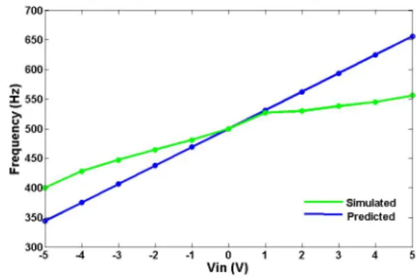
The performance of the Voltage Controlled Oscillator: The VCO has a power consumption of 1.3 mW. The variation of frequency has a slight deviation from calculated values in Fig.9, due to non-idealities of the devices and circuits. The linearity between the input voltage Vin of Fig.1 and the
frequency of Voutis evident from the graph and is in agreement
with (6).
It should be noted that the semiconductor is amorphous in nature and the field-effect mobility is around 10 cm2/V.s. This
device inferior performance lead to low frequency of oscilla-tion. Further improvement in the phase noise can be obtained by using design techniques consists of two comparators [9]
IV. CONCLUSIONS
This paper presented a voltage controlled oscillator with IGZO TFTs for the first time, which is capable of generating variable frequencies by tuning the voltage. The circuit can be used as on-chip oscillator with frequency tuning ability or as frequency divider (refering to relaxation oscillator) in
Fig. 9. Plot between the simulated and predicted values of VCO
flexible large-area systems, such as, smart packaging, wearable electronics and biomedical applications.
ACKNOWLEDGMENT
This work is supported by early career research grant with project ref. ECR/2017/000931. This work is also funded by FEDER funds through the COMPETE 2020 Programme and National Funds through FCT - Portuguese Foundation for Science and Technology under the projects numbers POCI-01-0145-FEDER-007688, Reference UID/CTM/50025 and UID/EEA/00066/2013. This work also received funding from the European Communitys H2020 program under grant agreement No. 716510 (ERC-2016-STG TREND), No. 644631 (Roll-Out) and No. 692373 (BET-EU).
REFERENCES
[1] K. Nomura, H. Ohta, A. Takagi, T. Kamiya, M. Hirano, and H. Hosono, “Room-temperature fabrication of transparent flexible thin-film transis-tors using amorphous oxide semiconductransis-tors,” Nature, vol. 432, no. 7016, pp. 488–492, 2004.
[2] Y. Chen, D. Geng, M. Mativenga, H. Nam, and J. Jang, “High-speed pseudo-CMOS circuits using bulk accumulation a-IGZO TFTs,” IEEE Electron Device Letters, vol. 36, no. 2, pp. 153–155, 2015.
[3] A. Suresh, P. Wellenius, V. Baliga, H. Luo, L. M. Lunardi, and J. F. Muth, “Fast all-transparent integrated circuits based on indium gallium zinc oxide thin-film transistors,” IEEE Electron Device Letters, vol. 31, no. 4, pp. 317–319, 2010.
[4] D. Geng, D. H. Kang, and J. Jang, “High-performance amorphous indium–gallium–zinc–oxide thin-film transistor with a self-aligned etch stopper patterned by back-side uv exposure,” IEEE Electron Device Letters, vol. 32, no. 6, pp. 758–760, 2011.
[5] M. Mativenga, M. H. Choi, J. W. Choi, and J. Jang, “Transparent flexible circuits based on amorphous-indium–gallium–zinc–oxide thin-film transistors,” IEEE Electron Device Letters, vol. 32, no. 2, pp. 170– 172, 2011.
[6] Y. Chen, D. Geng, T. Lin, M. Mativenga, and J. Jang, “Full-Swing Clock Generating Circuits on Plastic Using a-IGZO Dual-Gate TFTs With Pseudo-CMOS and Bootstrapping,” IEEE Electron Device Letters, vol. 37, no. 7, pp. 882–885, 2016.
[7] P. Bahubalindrun, V. Tavares, P. Barquinha, P. G. De Oliveira, R. Martins, and E. Fortunato, “InGaZnO TFT behavioral model for IC design,” Analog Integrated Circuits and Signal Processing, vol. 87, no. 1, pp. 73–80, 2016.
[8] Y.-C. Tarn, P.-C. Ku, H.-H. Hsieh, and L.-H. Lu, “An amorphous-silicon operational amplifier and its application to a 4-bit digital-to-analog converter,” IEEE Journal of Solid-State Circuits, vol. 45, no. 5, pp. 1028–1035, 2010.
[9] P. F. Geraedts, E. van Tuijl, E. A. Klumperink, G. J. Wienk, and B. Nauta, “A 90µW 12MHz Relaxation Oscillator with a-162dB FOM,” in Solid-State Circuits Conference, 2008. ISSCC 2008. Digest of Technical Papers. IEEE International. IEEE, 2008, pp. 348–618.