Jean Carlos da
Conceição Lorenzzi
Boron nitride thin films deposited by magnetron
sputtering on Si
3N
4Filmes finos de nitreto de boro depositados por
pulverização catódica em Si
3N
42007
Jean Carlos da
Conceição Lorenzzi
Boron nitride thin films deposited by magnetron
sputtering on Si
3N
4Filmes finos de nitreto de boro depositados por
pulverização catódica em Si
3N
4Dissertação apresentada à Universidade de Aveiro para cumprimento dos requisitos necessários à obtenção do grau de Mestre em Engenharia e Ciência dos Materiais, realizada sob a orientação científica do Dr. Rui Ramos Ferreira e Silva, Professor Associado do Departamento de Engenharia Cerâmica e do Vidro da Universidade de Aveiro .e do PhD. Jens H. Andreasen, Professor Associado do Departamento de Egenharia Mecânica da Universidade de Aalborg – Dinamarca.
It doesn’t matter how beautiful your theory is, It doesn’t matter how smart you are.
If it doesn’t agree with experiment, it’s wrong.
o júri
presidente Prof. Dr. Vitor Brás Sequeira Amaral
Professor associado da Universidade de Aveiro
Prof. Dr. José Manuel de Oliveira Castro Castanho
Professor auxiliar da Faculdade de Ciências e Tecnologia da Universidade de Coimbra
Prof. Dr. Rui Ramos Ferreira e Silva
Acknowledgments
Agradecimentos There are many people that must be acknowledged for their technical andmoral support that led to the completion of this work. I wish to express my sincere appreciation to everyone who contributed to this study.
First, I would like to express my gratitude to my supervisors PhD. Professor Rui Ramos Ferreira e Silva for giving me an opportunity to work under his guidance and also for assigning me to this very interesting project.
Then, I would like to thank Assoc. Professor PhD. Jens H. Andreasen, my Co-supervisor, for his guidance during the EMMS mobility in Aalborg-Denmark. A special acknowledgement goes to PhD. Mercedes Vila, who has always put aside her own projects to help me when I needed assistance. Her vast experience and creativity helped me greatly along the way, and it was essential to the completion of this thesis.
Special thanks to PhD. Filipe Oliveira for his strong support and advices, especially during those moments when my brain was out of order.
I would also like to acknowledge the technical assistance from PhD. Professor Armando Lourenço for sharing the experience in thin films by R.F. magnetron sputtering and also for his invaluable help during those long depositions. I would also like to express my thanks to Dr. Carlos Miguel Cardeal Enes Granadeiro, Ricardo João Borges Pinto for their help during the FTIR characterisation, Dra. Rosário Soares for her strong support during the XRD measurements and Prof. Dr. Albano Cavaleiro for his support during the mechanical characterisation.
To my fellow colleagues, António José Fernandes, Diogo Mata, MSc. Ermelinda Salgueiredo, Micaela Sousa, MSc. Filipa Neves, MSc. Flávia Almeida, Eng. Paulo Duarte, PhD. Margarida Amaral, at the Diamond Group of Ceramic and Glass Engineering Department, thanks for being there and providing support when I needed.
I would also like to thank my EMMS colleagues Eng. Júlio César Longo, Eng. Fábio Bertocco, Gil Gonçalves, Eng. Marcos Ghislandi, for their friendship and help, and also for many inspiring discussions.
The financial support of the Erasmus Mundus Programme is gratingly acknowledged.
And last, but not least, my Family Inês Wollinger da Conceição, Vilson José Lorenzzi, Elzira Wollinger da Conceição, João Maria da Conceição, Ana Carla da Conceição Lorenzzi and Estelle Mairesse who supported me during all this time and helped me overcome to my problems.
Sincerely Jean Carlos da Conceição Lorenzzi Aveiro, September 2007
Palavras-chave Filmes de nitreto de boro, Si3N4, Magnetron sputtering, FTIR, Nanodureza e tensões residuais
Resumo O Nitreto de boro é um material polimorfo, sendo as fases hexagonal (h-BN) e cúbicas (c-BN) as predominantes. A fase hexagonal do nitreto de boro apresenta uma estrutura em camadas sp2, semelhante a grafite, enquanto que a fase cúbica do nitreto de boro tem forte ligações sp3, como o diamante. O h-BN apresenta boas propriedades dieléctricas, é um material refractário, resistente a corrosão, é conhecido por ser um lubrificante sólido que tem aplicações na protecção de moldes de injecção e em outros processos mecânicos de elevadas temperaturas ou lubrificação em ambientes de elevada humidade. Contudo, o h-BN é extremamente macio. Em contraste, o c-BN apresenta excelentes propriedades térmicas, eléctricas e ópticas, sendo ainda um dos materiais conhecidos com dureza mais elevada (70 GPa). Além disso, c-BN apresenta propriedades superiores em relação ao diamante quando aplicado em ferramentas de corte na maquinagem de materiais ferrosos, devido a sua alta estabilidade química a altas temperaturas durante a maquinagem. Essa combinação de propriedades faz dele um forte candidato no campo das ferramentas de corte e em dipositivos electrónicos. No presente trabalho, filmes finos de nitreto de boro foram depositados por DC e RF magnetron sputtering, utilizando alvos de B4C e h-BN prensados a quente, numa atmosfera de deposição contituída por misturas de Ar e N2. Os filmes finos de BN foram depositados simultâneamente em dois tipos de substratos: cerâmicos de Si3N4 com diferentes acabamentos superficiais e em discos de Si(100). A influência dos parâmetros de deposição, tais como a temperatura do substrato, composição da atmosfera de deposição na espessura dos filmes, taxa de deposição, cristalinidade, tensão residual, fases presentes e dureza, foram sistematicamente investigados usando técnicas como, SEM, XRD, FT-IR e nanodureza. O h-BN foi a principal fase observada nas análises dos espectros de FT-IR e nos difractogramas de XRD. O estado de tensão dos filmes finos de BN films é estremamente afectado pela temperatura do substrato, composição do gás de trabalho e pelo acabamento superficial dos substratos. O estudo da influência da temperatura mostraram que a taxa de deposição aumenta com o aumento da temperatura do substrato. Tensões residuais elevadas ocorrem para altas concentrações de árgon e para substratos polidos em suspensão de diamante 15 μm. Nos espectros de FT-IR, a forma das bandas de vibração variam de uma forma alargada para uma configuração estreita, correspondendo a uma menor desordem da fase hexagonal do BN, devido a variação da composição da atmosfera de deposição. Os valores de dureza obtidos estão numa faixa que vai desde os valores do h-BN macio (6 GPa) até valores próximos dos limites encontrados para filmes contendo a fase cúbica (16 GPa ), acima de 40%.
Keywords BN thin films; Si3N4 substrate; magnetron sputtering; FTIR, Nanohardness and films stress.
Abstract Boron nitride is a polymorphic material, the hexagonal (h-BN) and the cubic (c-BN) being its main crystalline structure. The hexagonal boron nitride has a layered sp2-bonded structure, similar to graphite, while the cubic boron nitride has a hard sp3-bonded diamond-like structure. h-BN presents good dielectric properties, refractoriness, corrosion-resistant characteristics, low friction and low wear rate, and it is a well-known solid lubricant which has wide applications in metal-forming dies and other metal working processes at high temperatures or lubrication in high relative humidity environments. However, h-BN is mechanically soft. In contrast, c-BN presents excellent thermal, electrical and optical properties, with a hardness up to 70 GPa. Moreover, c-BN is superior to diamond as cutting tool for ferrous materials due to its high thermal chemical stability during machining. In the present work, thin films of boron nitride have been deposited by D.C. and R.F. magnetron sputtering from hot-pressed B4C and h-BN targets, using mixtures of Ar and N2, as working gases. The BN thin films were deposited simultaneously on two different substrates: Si3N4 ceramics with different surface finishing and Si(100) wafers. The influence of parameters such as substrate temperature and working gas composition ratio, on film thickness, deposition rate, cristallinity, residual stress, phase composition and hardness, were systematically investigated using techniques like SEM, XRD, FT-IR and nanohardness. h-BN was the main observed phase. The stress-state of the thin BN films is largely affected by the substrate temperature, working gas composition and the substrate surface finishing. The substrate temperature studies show that the deposition rate increases with an increasing of the substrate temperature. Large high residual stresses are developed for higher argon ratios and for substrate finishing with 15 μm diamond paste. In the FT-IR spectra, the shape of the vibration band changes from broad to narrow, corresponding to a less disorder h-BN phase, due to the working gas composition. The hardness values obtained are typical in the range of a soft h-BN (6 GPa) to values approaching the limit of the range reported for films containing a fraction of cubic phase (16 GPa ) up to 40%.
Contents
Chapter 1 - Introduction
……….……… 1Chapter 2 - Literature review
………..…... 42.1. Silicon nitride ……… 4
2.2. Boron nitride (BN) ……….… 9
2.3. Sputtering technique ……….…...……. 11
2.4. Boron nitride thin films ………...……….… 18
Chapter 3 - Experimental methods and characterisation techniques
… 213.1. Silicon nitride substrates (Si3N4) ………..…….... 21
3.1.1. Production of silicon nitride substrates ……… 21
3.1.2. Characterisation of silicon nitride substrates ………….…....… 23
3.2. BN thin films ……….……….….…… 25
3.2.1. Production and characterisation of the targets …….……...… 25
3.2.2. Coating deposition ………. 26
3.2.2.1. DC magnetron sputtering ………. 26
3.2.2.2. RF magnetron sputtering ………...…..… 28
3.2.3. Coating characterisation methods ……….….…….. 31
Chapter 4 – Results and Discussion
………..……….. 324.1. Silicon nitride substrates (Si3N4) ……….……..….... 32
4.2. Boron nitride thin films ……….………..… 37
4.2.1. Targets characterisation ……….. 37
4.2.2. DC magnetron sputtering ……….…… 39
4.2.3. RF magnetron sputtering ……….… 41
4.2.3.2. Working gas composition studies ……….… 50
Chapter 5 – Conclusions
……….……. 58Chapter 6 – Recommendation of future work
…………...……….. 60List of Figures
Fig. 1.1 - Fig. 2.1 - Fig. 2.2 - Fig. 2.3 - Fig. 2.4 - Fig. 2.5 - Fig. 2.6 - Fig. 2.7 - Fig. 2.8 - Fig. 3.1 - Fig. 3.2 - Fig. 3.3 - Fig. 3.4 - Fig. 3.5 - Fig. 3.6 - Fig. 3.7 - Fig. 3.8 - Fig. 4.1 - Fig. 4.2 - Fig. 4.3 - Fig. 4.4 - Fig. 4.5 -Illustration of new challenges related to thin films materials and devices [4] ………. Crystal structures of trigonal α-Si3N4 (space group P31c and with lattice parameter
a=0.7818 and c= 0.559) and hexagonal β-Si3N4 (space group P63/m and with lattice
parameter a=0.7595 and c= 0.29023), emphasizing the corner-sharing SiN4 tetrahedra
[16] ……….. Typical microstructure of a liquid-phase sintered Si3N4ceramics; (a) schematic and (b)
SEM micrograph [17], where: 1- Si3N4matrix grains, 2-crystalline secondary phase,
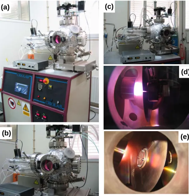
3-amorphous phase at triple junctions and grain boundaries ……… Structures of sp3-bonded and sp2-bonded phases for BN with their respective stacking sequences [39] ……….. Schematic representation of a crystal structure of c-BN [39] ………. Schematic diagram of a sputtering deposition [49] ………. Depiction of energetic particle bombardment effects on surfaces and growing films [50] … Schematic diagram of deposition on an on-axis mounted substrate [54] ……… Schematic deposition chamber and off-axis RF magnetron sputtering technique [55] ……. (a) graphite resistance heated furnace used to sinter the substrates, (b) uniaxial pressing mould, and (c) view of Si3N4 substrates after sintering ………..
Schematic diagram of the sintering cycle of silicon nitride (Si3N4) substrates ………
Flow chart for the preparation of Si3N4 substrates ………..
(a) SEM of a Vickers indentation defining indent and median crack parameters "a" and "c", respectively; (b) view of the cracks around a Vickers indentation ………. (a) Schematic diagram of HP cycle of the BN targets and (b) HP targets produced ………. Different views of the experimental set-up for the D.C. magnetron sputtering deposition from Physical Department at Aveiro University ………. Different views of RF magnetron sputtering equipment from Physics Department of Aveiro University ……… Schematic diagram of the BN thin film deposition system ………. (a-b) Scanning Electron micrographs of the sintered Si3N4 ceramics without surface
etching ……… SEM micrograph of Si3N4 after etching in (a) H3PO4 and (b) etched by CF4 plasma ………
(a-b) SEM micrograph of the fracture surface of the Si3N4 ceramic after etching in H3PO4.
X-ray Diffraction pattern of the powders mixture and the sintered Si3N4 using CuKα
radiation ………..
The FTIR absorption spectra for Si3N4 substrates ………..
1 5 7 9 11 12 13 15 17 22 23 23 25 26 27 28 29 33 33 34 34 35
Fig. 4.6 - Fig. 4.7 - Fig. 4.8 - Fig. 4.9 - Fig. 4.10 - Fig. 4.11 - Fig. 4.12 - Fig. 4.13 - Fig. 4.14 - Fig. 4.15 - Fig. 4.16 - Fig. 4.17 - Fig. 4.18 - Fig. 4.19 - Fig. 4.20 - Fig. 4.21 - Fig. 4.22 - Fig. 4.23 - Fig. 4.24 - Fig. 4.25 - Fig. 4.26 - Fig. 4.27 -
Scanning electron micrograph of Si3N4 indentation; (a) SEM of indentation, imprint (b)
SEM of an indentation crack ………... X-ray Diffraction pattern of h-BN hot-pressed target, using CuKα radiation. Intensity axis is in log (10) scale ………. X-ray Diffraction pattern of B4C hot-pressed target, using CuKα radiation. Intensity axis is
in log (10) scale ………. Fourier Transform Infrared (FTIR) absorption spectrum of h-BN hot-pressed target ……… Fourier Transform Infrared (FTIR) absorption spectrum of B4C hot-pressed target ………..
FTIR absorption spectra for BN films deposited by D.C. Magnetron sputtering under different conditions ……… SEM micrographs of the films deposited by DC sputtering at different conditions ………… FT-IR absorption spectra in transmittance mode of BN films deposited on Si3N4 substrates
(surface finishing 6μm) under different substrate temperatures ……… FT-IR absorption spectra in transmittance mode of BN films deposited on Si3N4 substrates
(surface finishing 15μm) under different substrate temperatures ………. Stress and peak position of the BN films deposited on Si3N4substrates (surface finishing
of 6 μm and 15 μm) under different substrate temperatures ………. FT-IR absorption spectra in transmittance mode of BN films deposited on Si(100) substrates under different substrate temperatures ……….. Glancing-angle X-ray Diffraction patterns of the BN film on Si(100) wafer substrates deposited at different substrate temperatures ……….. SEM micrographs of the surface of BN films on Si3N4 (surface finishing of 6 μm)
substrates deposited at different substrate temperatures ……….. SEM cross-sectional images of BN layer system on Si3N4 (surface finishing of 6 μm)
substrates deposited at different substrate temperatures ……….. Dependence of the thickness and deposition rate of BN thin films with substrate temperature (Ts) ……… Hardness and errors associate with the measurement as function of substrate temperature ……… FT-IR absorption spectra in transmittance mode of BN films deposited on Si3N4 substrates
(surface finishing of 6 μm) at 400ºC, using different working gas composition Ar/N2
(%vol.) ………. FT-IR absorption spectra in transmittance mode of BN films deposited on Si3N4 substrates
(surface finishing of 15μm) at 400ºC, using different working gas composition Ar/N2
(%vol.) ……….. Stress and peak position of the BN films deposited on Si3N4substrates (surface finishing
of 6 μm and 15 μm) under working atmospheres ratio (Ar/N2) ………..
FT-IR absorption spectra in transmittance mode of BN films deposited on Si(100) substrates at 400ºC, using different working gas composition Ar/N2 (%vol.) ………...
Glancing-angle (2º) X-ray diffraction patterns of the BN film on Si(100) wafer substrates deposited at 400ºC, using different ratios of Ar/N2 (%vol.) ………..
SEM micrographs of the surface of BN films on Si3N4 (surface finishing of 6 μm)
substrates deposited at 400ºC using gas mixtures of Ar/N2 (%vol.) as working gas …….. 36 37 38 38 39 40 41 43 43 44 45 45 47 48 49 50 51 51 52 53 54
Fig. 4.28 -
Fig. 4.29 -
Fig. 4.30 -
SEM cross-sectional images of BN layer system on Si3N4 (surface finishing of 6 μm)
substrates deposited at 400ºC using gas mixtures of Ar/N2 (%vol.) as working gas ……….
Dependence of the thickness and deposition rate of BN thin films with the N2 working gas
content ……… Hardness and errors associate with the measurement as function of working gas composition ………
55
56
List of Tables
Table 2.1 - Table 2.2 - Table 2.3 - Table 3.1 - Table 3.2 - Table 3.3 - Table 4.1 - Table 4.2 - Table 4.3 - Table 4.4 - Table 4.5 - Table 4.6-Typical properties (at room temperature) for hot-pressed and pressureless sintered silicon nitrides [17] ……….. Properties of BN Materials [40-47] ……….…... Comparison of physical properties of single-crystalline diamond and c-BN [45-47] ……. Composition and characteristics of the raw materials used to the produce Si3N4
substrates ……….. Deposition parameters for D.C sputtering using B4C target. (Ssf - substrate surface
finishing, DC - power applied to the target, Bias - bias applied to the substrate; Ar/N2
-gas composition, Pt - total pressure during deposition, , D-distance targesubstrate,
t-deposition time) ………. Deposition parameters for BN thin film deposition by RF sputtering using h-BN as target: (sb – Kind of substrate, Ssf – substrate surface finishing, RF -power applied to the target, Pt - total pressure during deposition, Ar/N2 – working gas composition, D
-distance target-substrate, t - deposition time, T - substrate temperature ) ………. Physical properties of silicon nitride used as substrates ……… Phase content and mechanical properties of silicon nitride substrates ………... Identification of the X-ray reflection planes, taken from Fig. 4.17, of the BN coating deposited on Si(100), substrate temperature studies ………... The physical and mechanical properties of BN thin films prepared by R.F magnetron sputtering using different substrate temperatures ………... Identification of the X-ray reflection planes, taken from Fig. 4. 26, of the BN coating deposited on Si(100), during the working gas (Ar/N2) ratio study ……….
The physical and mechanical properties of BN thin films prepared by R.F magnetron
sputtering using different working gas ratio (Ar/N2) ……….
7 10 11 21 27 30 32 36 46 49 54 56
List of Abbreviations
PVD CVD RF DC BN c-BN h-BN w-BN r-BN t-BN Si3N4 B4C HP HIP HT/HP GPS LPS IBAD PLD XRD SEM FT-IR KIC Hv E TO RTPhysical Vapour Deposition Chemical Vapour Deposition Radio frequency
Direct current Boron nitride Cubic boron nitride Hexagonal boron nitride Wurtzitic boron nitride Rhombohedral boron nitride Turbostratic boron nitride Silicon nitride
Boron carbide Hot pressing
Hot isostatic pressing
High temperature high pressure Gas pressure sintering
Liquid phase sintering Ion-beam assisted deposition Pulsed laser deposition X-ray Diffraction
Scanning Electron Microscopy Fourier transform Infrared Fracture Toughness (MPa.m1/2) Vickers Hardness (GPa) Young’s modulus (GPa) Transverse optical Room temperature
Introduction
The importance of synthesis of new coatings for the industry has resulted in a great increase of innovative thin film processing technologies. Presently, this progress goes hand-in-hand with the explosion of scientific and technological advances in microelectronics, optics and nanotechnology [1].
Thin films are essential in a significant number of components like, for example, thermal barrier coatings and wear protections, enhancing their service life by protecting materials against mechanical, thermal and atmospheric influences [2, 3]. Currently, the rapidly changing needs for thin film coated materials and devices are generating new opportunities for the development of new solutions. Fig. 1.1 shows the elements that undergo the Thin Film Science.
Fig. 1.1 – Illustration of new challenges related to thin films materials and devices [4].
It is very well known that cubic boron nitride (c-BN) is one of the hardest materials. It is a promising candidate as hard coating for cutting tools due to its extreme properties, similar to those of diamond in terms of hardness, thermal conductivity and optical transparency. But it has two advantages in comparison with diamond: i) c-BN is chemically inert in oxygen
atmospheres, even more stable against oxidation up high temperature than diamond; ii) boron and nitrogen atoms do not diffuse into ferrous [5] substrate materials under thermal loading, contrarily to carbon in diamond. Therefore, c-BN seems to be better suited for wear protection films on steel substrates [6].
These properties make c-BN a potential candidate for many thin film applications not only, as wear protecting layers on tools, but also as transparent protecting films on optical components or as heat dissipating films in electronics and laser diode technology. However, a disadvantage of c-BN is their cost and processing complexity.
In many cutting and forming operations, coated tools are indispensable for industrial production. Hard coatings for wear reduction, like TiN, TiCN, CrN and TiAlN or dry lubricant coatings like MoS2 are well established [7]. One consequence of increasing the productivity and product quality is the need to increase the tool performance. Particularly, the trend to operate under dry conditions, high speed cutting, cutting of hard materials, and machining of lightweight materials is still a challenge for the development of new tools and coatings.
The synthesis of c-BN can be performed in different ways, classically in bulk form at high temperature and high pressure (HT/HP), but to obtain thin films, PVD and CVD are the most common. Magnetron sputtering is a PVD method involving the removal of material from a solid cathode, while the substrate is placed in a low-pressure chamber between two electrodes assisted by a magnetron. It is commonly used for thin film deposition at room temperature.
In many cases, magnetron sputtered films now outperform films deposited by other PVD processes, and can perform the same functionality as much thicker films produced by other surface coating techniques. Consequently, magnetron sputtering has now a significant impact in application areas including hard, wear resistant coatings, low friction coatings, corrosion resistant coatings, decorative coatings and coatings with specific optical or electrical properties [8].
The commonly used magnetron sputtering techniques are: (i) Radio Frequency (RF) sputtering by applying a RF signal to the electrode (target) it can be used for both conductor and insulator targets; (ii) Direct current (DC) sputtering by applying a DC voltage to the electrode it can only be used with conducting targets and (iii) Reactive sputtering where a reactive gas is used with a inert gas during the deposition.
The deposition of boron nitride films by DC and RF magnetron sputtering envisaging enhanced wear resistance of industrial components namely, cutting tools, was thus the aim of the present work. This technique presents a great interest for industrial applications, due to its low work temperature and up scaling potential.
The BN thin films, partially comprising the c-BN phase, were produced in the Ceramic and Glass Engineering Department and in the Physics Department of Aveiro University.
Primary studies were performed using DC magnetron sputtering using B4C as target, but this technique was put aside because of some equipment restrictions. For this reason, RF magnetron sputtering was performed from a hot-pressed h-BN disc target.
The deposition processes were carried out in two different vacuum chambers (for DC and for RF magnetron sputtering), with mixtures of Ar and N2 as working gases. Several parameters were altered during film depositions in order to optimise the BN growth.
BN thin films (thickness between 180-500 nm) were grown on Si(100) wafers and silicon nitride (Si3N4) substrates, simultaneously. The use of silicon nitride as a substrate is related to its superior properties - high fracture toughness and mechanical strength, thermal shock resistance, good creep behaviour - and potential high interface compatibility with BN, similar to that with the diamond [9]. The Si3N4 ceramic substrates discs with a diameter of 10 mm were prepared by the powder technology at Aveiro University in the Ceramic and Glass Engineering Department. The Si(100) wafers were used as substrate in order to provide a support during the characterisation.
The characterisation of the Si3N4 substrates and the BN films was made at the Institute of Mechanical Engineering in Aalborg University, Denmark and also at Aveiro University. Several techniques were used in order to characterise the substrates and coatings, namely: Fourier Transform Infrared (FT-IR), X-ray diffraction (XRD) using the glancing incidence angle configuration, Scanning Electron Microscopy (SEM) and nanohardness.
Literature Review
The purpose of this chapter is to resume the most important theoretical concepts for interpretation of the experimental data on silicon nitride substrates processing and BN coating growth and properties. The chapter is divided into four parts. In the first and second ones, some background about silicon nitride and boron nitride compounds is presented. The third part reports the main concepts of Physical Vapour Deposition (PVD) chosen as coating technique in this work. The last section is an overview on literature concerning BN thin films.
2.1. Silicon
nitride
Silicon nitride (Si3N4) was developed in the 1960s and 1970s in a search for fully dense, high strength and high toughness materials [10]. A prime driver for its development was to replace metals with ceramics in advanced turbine and reciprocating engines to give higher operating temperatures and efficiencies. Although the ultimate goal of a ceramic engine has never been achieved, silicon nitride ceramics have been used in a number of industrial applications, such as engine components, bearings and cutting tools for machining cast irons and nickel-based alloys [11, 12].
Silicon nitride is a polymorphic material, presenting three crystallographic modifications designated as the α, β and γ phases. While the α and β modifications can be produced under normal nitrogen pressure and have great importance in the production of advanced ceramics, the recently discovered γ-Si3N4 can be formed only at extremely high pressures [13] and has no practical use yet.
In a simple chemical picture, chemical bonding in α- and β- Si3N4 are due to the overlap of the sp3 hybrid orbitals of silicon atoms with the sp2 hybrid orbitals of the nitrogen atoms. Each nitrogen atom has a remaining p atomic orbital which is nonbonding and that is occupied by a single pair of electrons [13, 14].
The basic unit of Si3N4 is the SiN4 tetrahedron. A silicon atom is located at the centre of a tetrahedron, with four nitrogen atoms at each corner. The SiN4 tetrahedra are joined by sharing corners in such a manner that each nitrogen is common to three tetrahedra. Thus nitrogen has three silicon atoms as neighbours [15]. The structural difference between α- and
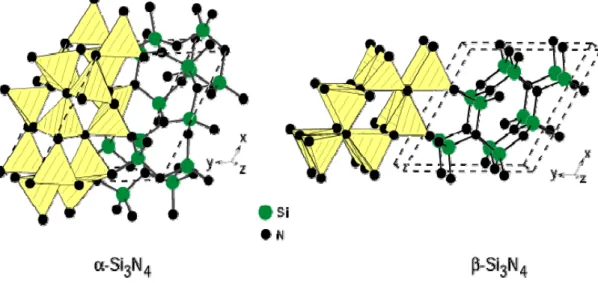
β- Si3N4 can be explained by different arrangements of Si-N layers, as it can be seen in Fig. 2.1. The basic units are linked together to form puckered six-membered rings which surround large holes. These basal planes form the building blocks for the structures of α and β- Si3N4.
Fig. 2.1 - Crystal structures of trigonal α-Si3N4 (space group P31c and with lattice parameter a=0.7818
and c= 0.559) and hexagonal β-Si3N4 (space group P63/m and with lattice parameter a=0.7595 and c=
0.29023), emphasizing the corner-sharing SiN4 tetrahedra [16].
The α- Si3N4 structure is formed by stacking the basal planes in the ABCDABCD... order, and β- Si3N4 is constructed of basal planes stacked in the ABAB... sequence [17]. The AB layer is the same in α- Si3N4 and β- Si3N4, and the CD layer in α- Si3N4 is related to the AB layer of β- Si3N4 by a c-glide plane. Regarding the unit cell dimensions, α- and β- Si3N4 structures are related by Aα ≈ Bβ.
The β- Si3N4 structure exhibits channels parallel to the c-axis which are about 0.15 nm in diameter enabling higher diffusion coefficients of ions when compared to the α-structure. These channels are changed into voids with seven nearest neighbouring nitrogen atoms in α-Si3N4. The α- and β-forms have trigonal and hexagonal symmetry, respectively.
The high degree of covalent bonding makes it very difficult to produce pure dense Si3N4 ceramics by solid state sintering. The main reason for this relies on the fact that the diffusion of silicon and nitrogen in the volume or at the grain boundaries of Si3N4 is extremely slow [18]. The densification of Si3N4 is thus conducted via the presence of a liquid phase with the help of oxide additives
At the sintering temperatures, typically in the range 1550 – 1750 ºC, the oxide additives react with the silica present on the Si3N4 powder particles, forming an oxynitride liquid phase which acts as mass transport medium [19]. However, at high temperatures Si3N4 starts to dissociate [20].
Many studies have been reported on Si3N4 ceramics with Y2O3 and Al2O3 as sintering additives because of their excellent sinterability and mechanical properties, such as bending
strength and fracture toughness. It is generally recognised that the kind and amount of sintering additives, as well as raw materials and sintering conditions, greatly affect the microstructure after sintering [21,22]. As a consequence, many different sintering techniques have been developed.
One common densification method is the nitridation of silicon compacts, leading to Reaction-Bonded silicon nitride materials. By this method, complex shapes can be produced using various ceramic forming methods (slip casting, injection moulding, die pressing, isostatic pressing) with low costs. However, the process leads to a material of limited density (about 70-88%) resulting in poor mechanical properties. Because of the residual porosity the strength of the reaction bonding silicon nitride materials is relatively low. Furthermore, the pore structure goes ahead to high oxidation rates and to small erosion resistance [23, 24]. Thus, low densities and pore structure limit the range of possible applications of the reaction bonding silicon nitride materials.
Hot-pressing (HP) of pure silicon nitride powder at high temperatures does not result in full density and also leads to the production of porous materials with properties similar to those of the reaction bonding silicon nitride [25]. In spite of this, the first dense Si3N4 ceramic was that accomplished by uniaxial hot pressing Si3N4 powders containing MgO as sintering additive [26]. Such kind of hot-pressed Si3N4 ceramics is a high strength material, which can be used at temperatures up to 1000°C without a decrease in strength. Because of high cost and difficulties to machine the components, hot-pressing, today, has limited use for the production of simple shaped parts and low quantities.
Another method used to produce dense Si3N4 material is by applying an isostatic pressure (>100 MPa) instead of uniaxial pressure, i.e. hot-isostatic pressing (HIP). During this process a high gas pressure is applied to consolidate a powder compact or to remove the residual porosity from pre-sintered bodies. The uniform manner of applying the high pressure results in fully isotropic material properties. The possibility to use much higher pressures than in uniaxial hot-pressing leads to an enhancement in the densification of the products. Thus, fully dense ceramic parts can be produced from powders of lower sintering activity and with smaller amounts of additives when compared with uniaxial hot pressing. Resulting materials combine excellent mechanical and thermo-mechanical properties, but the cost of the process is relatively high.
Another sintering method for high-strength Si3N4 ceramics is the gas pressure sintering (GPS), under 10 MPa. This method allows sintering of the complex-shaped parts with medium cost. However, the most economical method to sinter Si3N4 powder compacts with additives at atmospheric pressure and temperature around 1700°-1800°C, is pressureless sintering (PS).
In this study, the silicon nitride substrates were consolidate using PS technique. The resulting microstructure of dense Si3N4 consists mainly of β-Si3N4 grains and a mostly
amorphous grain-boundary phase in the form of thin layers or at triple junctions, Fig. 2.2a. During cooling or after heat treatment, crystalline secondary phases may arise in the intergranular transient (Fig. 2.2). This intergranular phase strongly affects the mechanical properties, especially at high temperatures. The thickness of the grain boundary film depends either on the types of additives as on the amount of liquid phase.
A typical feature of sintered Si3N4 ceramics is the morphology of the Si3N4 grains (Fig 2.2b). Residual α-grains are equiaxial while the β-phase exhibits an elongated grain structure with an aspect ratio (ratio between length and thickness) usually in the range of 5 to 10 [27]. The microstructural development is controlled mainly by the Si3N4 starting powders, the additives used and the sintering parameters.
Fig. 2.2 - Typical microstructure of a liquid-phase sintered Si3N4ceramics; (a) schematic and (b) SEM
micrograph [17], where: 1- Si3N4matrix grains, 2-crystalline secondary phase, 3-amorphous phase at
triple junctions and grain boundaries.
Typical data for the properties of hot-pressed and pressureless sintered Si3N4 are presented in Table 2.1.
Table 2.1- Typical properties (at room temperature) for hot-pressed and pressureless sintered silicon nitrides [17].
Property Hot pressed Si3N4 Pressureless sintered Si3N4
Density(g/cm3) >3.20 3.20
Thermal conductivity (W/mK) 29.3 15.5
Flexural strength (MPa) 1200 800
Compressive strength (MPa) 4500 4000
Thermal expansion (10-6/K) 3.2 3.4
Young’s modulus (GPa) 320 280
Toughness-KIC(MPa.m1/2) 8.3 5.4
Hardness (GPa) 18 16
It can be inferred from the given data, (Table 2.1) that Si3N4possesses high strength, good thermal-shock resistance due to the low coefficient of thermal expansion. Moreover, it
(b)
(a)
has a high resistance to oxidation when compared to other high-temperature structural materials [28].
The mechanical properties of Si3N4 ceramics depend on the presence of pores, cracks and inclusions. Among these factors, porosity has been demonstrated to have a pronounced effect on mechanical strength. Fracture toughness differs mainly with variations in the microstructure. The grain shape and size along with the phase composition of the grain-boundary phase have a strong influence. High fracture toughness of Si3N4based ceramics could be explained on the basis of similar toughening mechanisms as in whisker reinforced composite materials (grain bridging, pull-out, crack deflection, and crack branching [29]). However, these toughening mechanisms are only active when the dominant fracture mode is intergranular.
The ratio between transgranular and intergranular fracture depends on the strength of both intergranular phase and Si3N4grains. A material with higher toughness has a weaker grain boundary. On the other side, the strength of the grain-boundary phase is connected with the local residual stresses [30]. When the thermal expansion coefficient of the grain-boundary phase is higher than that of the Si3N4grains, the grain-boundary phase is under tensile stress and the fraction of intergranular fracture is higher. As a consequence, the fracture toughness increases. In contrast, ceramics with a grain boundary phase under compression have low fracture toughness because of a higher amount of transgranular fracture [31].
Thermal conductivity is another interesting property of Si3N4which combined with the excellent mechanical properties makes it a serious candidate for high-performance substrates under thermo dynamical loading [32].
2.2. Boron nitride (BN)
The elements boron and nitrogen, both neighbours to carbon in the Periodic Table, form 1:1 compounds, which are microstructural and isoelectronic to the polymorphs of carbon. The hexagonal modification of boron nitride (h-BN) has a layered sp2-bonded structure similar to graphite (Fig. 2.3a) and it is sometimes called “white graphite” [33]. Hexagonal BN was prepared for the first time in the mid-19th century [34, 35]. It remained a laboratory curiosity for more than hundred years, until hot-pressed h-BN shapes were firstly made in 1957 [36]. Hexagonal boron nitride is the only BN phase found in nature. The cubic modification (c-BN) is a hard sp3-bonded diamond-like phase with a cubic zinc-blende structure (Fig. 2.3d). In 1957, cubic BN was first grown in bulk crystalline form by using a high pressure and high temperature method [37]. In 1970, c-BN thin films deposited by a physical vapour deposition (PVD) were presented. Hexagonal and cubic BN are the only two stable phases of boron nitride.
The stacking sequences in h-BN and c-BN can vary, producing also metastable sp2- and sp3-bonded poly-types. By rearranging the basal planes of sp2-bonded BN in a staggered arrangement, rhombohedral BN (r-BN) is obtained (Fig. 2.3b). The metastable sp3-bonded modification of boron nitride is wurtzitic BN (w-BN, Fig. 2.3.c).
As with graphitic carbon, sp2-bonded boron nitride is often found in a disordered, turbostratic form (t-BN). This is the most commonly observed form of sp2-bonded material in boron nitride thin films. For a turbostratic structure, the two-dimensional in-plane order of quasi-hexagonal basal planes is largely retained, but these planes are stacked in a random sequence and with random rotation around the c-axis [38]. Thin films of boron nitride may also be formed without a distinct crystallographic order and without any distinctly identified phase. The films are then defined as amorphous boron nitride (a-BN).
Fig. 2.3 - Structures of sp3-bonded and sp2-bonded phases for BN with their respective stacking sequences [39].
Hexagonal boron nitride is widely used because of its combination of properties, e.g., low density, high temperature stability, chemical inertness, stability in air up to 1000°C, stability to thermal shock, easy workability of hot-pressed shapes, excellent electrical insulating character, very high thermal conductivity [33,39]. Bulk h-BN can therefore be used as a solid lubricant and as a ceramic insulating material in high temperature environments. It
can also be employed as a crucible for melting glass and metals, and as a neutron absorber and shield for nuclear reactors. A comprehensive list of physical properties of the most important phases of BN can be found in several material handbooks, and a short list of data is compiled in Table 2.2.
Table 2.2 - Properties of BN Materials [40-47].
Property c-BN h-BN a-BN
Space group cubF43m (216) P63mc (186)
Crystal structure cubic hexagonal zinc blende amorphous Lattice constant (Å) a = 3.6158 a = 2.50475
c = 6.6482
Density (g/cm3) 3.48 2.2 1.74
Hardness (GPa) 40–60 1-6 2-6
Band gap activation energy (eV) 0.19–0.23 0.05–0.41
Thermal conductivity (W.cm-1K-1) 2–9 0.68 0.36
Oxidation stability (ºC) 1200 - -
Elastic modulus (GPa) 850 30-100 -
Linear thermal expansion (10-6 K-1) 4.8 (700 K) 3.8 -
The cubic boron nitride (c-BN) form was first produced in 1957 by Robert H. Wentorf, a physical chemist for the General Electric Company [37], just two years after the first artificial diamonds were synthesized [42]. In analogy to the fabrication of diamond crystals, c-BN was produced from hexagonal boron nitride submitted to high pressure and high-temperature (HP/HT) conditions.
The interest in c-BN has increased tremendously since the late 1980’s, which is directly related to the fact that c-BN thin films can be routinely synthesized by a large variety of physical and chemical vapour deposition techniques.
The crystal structure of c-BN can be seen in the Fig. 2.4 [43] and consists in two unit cells of the cubic structure that are shown at the right-hand side. In the middle, the structure is projected along one of the threefold axes (cube diagonal). At the left-hand side, the tetrahedral environments around one kind of atoms are emphasized. Boron and nitrogen atoms occupy equivalent positions; hence the structure may be thought to be composed of NB4/4 as well as BN4/4 tetrahedra.
After diamond, it is one of the hardest materials known, with roughly 50-70 GPa Vickers hardness. However, c-BN exhibits a much better chemical inertness and thermal stability. Diamond readily reacts with iron, cobalt, and nickel at temperatures above 1000ºC or is subject to oxidation at temperature higher than 800ºC, which results in a disintegration of the diamond surface into gaseous CO2. In contrast, c-BN is chemically inert against iron group metals for temperatures of up to 1800ºC [43], and its high stability against oxidation is a
consequence of the formation of liquid or solid B2O3, which protects the surface against further oxidation [44].
Fig. 2.4 - Schematic representation of a crystal structure of c-BN [39].
Cubic boron nitride also has the potential to outclass diamond concerning electronic applications. It not only has a high band-gap and the second highest room temperature thermal conductivity after diamond, but, in contrast to diamond, it can be easily doped to obtain both n- and p-type conductivities [45, 46]. However, large scale industrial applications are still not possible, mainly because the c-BN crystals exhibit a rather high defect density and impurity concentration. A comparison between c-BN and diamond is given in Table 2.3.
Table 2.3 - Comparison of physical properties of single-crystalline diamond and c-BN [45-47]
Properties Diamond c-BN
Structure CubFd3m CubF43m (216)
Lattice constant (Å) 3.567 3.615
Interatomic distance (Å) 1.545 1.565
Atomic density (g/cm3) 1.77x10²³ 1.68x10²³
Density (g/cm3) 3.51 3.48
Hardness (GPa) 100 75
Elastic modulus (GPa) 1140 850
Thermal conductivity at RT (W/cm.K) 20-22 2-13 Thermal expansion coefficient (10−6K−1) 0.8 4.8
Melting point (K) 4027 3246
Oxidation stability (ºC) 600 1200
Band gap (eV) 5.45 6.4
2.3. Sputtering
technique
Sputtering is a PVD technique that involves the removal of material from a solid cathode, while the substrate is placed in a low-pressure chamber between two electrodes assisted by a magnetron. It is commonly used for thin film deposition at room temperature.
Sputtering is the phenomena of momentum transfer from an incident energetic projectile to a solid target resulting in the ejection of surface atoms or molecules. In the sputter deposition process, the target (a source of coating material) and the substrate are placed in the vacuum chamber and evacuated to a pressure typically in the range of10-4 to 10 -7 mbar [48].
A schematic diagram of the sputter coating process is shown in Fig. 2.5. Sputtering laboratory sources are usually magnetrons that use strong electric and magnetic fields to entrap electrons close to the surface of the magnetron, which is known as the target. They are connected to a negative voltage supply, and the substrate generally faces the target. A glow discharge is initiated after an inert gas (usually argon) is introduced into the evacuated chamber.
Fig. 2.5 - Schematic diagram of a sputtering deposition [49].
Non-metallic targets are generally prepared by hot-pressing of the powders. The metal and non-metals targets tend to have purities of 99.99% or higher. In addition, less than the theoretical densities are achieved during powder processing. These metallurgical realities are sometimes reflected in emission of particulates, release of trapped gases, non-uniform target erosion, and deposited films of inferior quality. Targets are available in a variety of shapes (e.g., disks, plates, etc.) and sizes. Prior to use, they must be bonded to a cooled backing plate to avoid thermal cracking and thermal degradation. Metal-filled epoxy cements of high thermal conductivity are employed for this purpose.
The number of atoms ejected from the surface per incident ion is called the sputter yield and is an important measure of the efficiency of the sputtering process. Besides, the sputter yield depends on the energy of the incident ions, the masses of the ions and target atoms, and the binding energy of the atoms in the solid [50].
Critical to the analysis and design of sputtering processes is an understanding of what happens when ions collide with surfaces [50]. Some of the interactions that occur are schematically shown in Fig. 2.6.
Fig. 2.6 - Depiction of energetic particle bombardment effects on surfaces and growing films [50].
Each interaction depends on the type of ion (mass, charge), the nature of the surface atoms involved, and, importantly, on the ion energy. Several of these interactions have been capitalised in widely used thin-film processing, deposition, and characterisation techniques [51].
Reactive Sputtering
Sputtering is an atomistic process and most of the atoms emitted from a target, regardless of whether it is an elemental or compound/alloy cathode, are emitted as atoms rather than molecules or clusters. Chemical reactions of these atoms moving from the cathode to the sample are rare, but it is completely possible that the freshly-deposited atom on a film surface chemically reacts with gas atoms that impinge on the surface to form a compound film. In other words, reactive sputtering can be explained as being the film deposition of compounds on substrates by sputtering from targets in the presence of a reactive gas, usually mixed with the inert working gas (invariably Ar).
There are two approaches to reactive deposition, one where the cathode is a metal plate, and the other where the cathode is composed by the material to be deposited, for instance, a nitride or an oxide. The most common compounds reactively sputtered (and the reactive gases employed) are briefly listed [52]:
• Oxides (oxygen) - Al2O3, In2O3, SnO2, SO2, Ta2O5; • Nitrides (nitrogen, ammonia) – BN, TaN, TiN, AlN, Si3N4; • Carbides (methane, acetylene, propane) - TiC, WC, SiC; • Sulfides (H2S) - CdS, CuS, ZnS;
The choice of whether to employ compound targets and sputter directly or sputter reactively is not always clear. If reactive sputtering is selected, then there is the option of using simple dc diode, RF, or magnetron configurations. Many considerations must be done before making these choices, such as [52]:
• Target purity - It is easier to manufacture purity metal targets than to make high-purity compound targets. Since hot pressed and sintered compound powders cannot be consolidated to theoretical bulk densities, the incorporation of gases, porosity, and impurities is inevitable. Film purity using elemental targets is high, particularly because high-purity reactive gases are commercially available.
• Deposition rates - Sputter rates of metals drop dramatically when compounds are formed on the targets. Decreases in deposition rate well in excess of 50% occur because of the lower sputter yield of the compounds relative to metals. The effect is very much dependent on the reactive gas pressure. Conditioning of the target in pure Ar is required to restore the pure metal surface and desired deposition rates. When high deposition rates are needed, the reactive sputtering mode of choice is either dc or RF magnetron.
• Stoichiometry and properties - Considerable variation in the composition and properties of reactively sputtered films is possible, depending on the operating conditions.
Magnetron Sputtering
The term “magnetron” was originally applied to describe tubes used to generate microwave power for radar applications. It is still used for this purpose, and the builder or owner of a microwave plasma system will use a “magnetron” power source to run the plasma. The same general magnetron effect found in these tubes can be somehow altered to make an extremely efficient sputtering cathode. These cathodes operate in a diode mode, either in RF or DC, but are rarely, if ever, called diodes. Magnetron sputtering sources are the current workhorse of the sputter deposition field, used in perhaps 95% of all sputtering applications.
The first paper on the magnetron as a sputtering device was reported in the 1960s [53]. Since then, magnetrons have suffered a continuous development in various industrial fields, especially microelectronic and surface processing, and are widely used for thin film deposition.
A magnetron uses a static magnetic field configured at the cathode location. The magnetic field is located parallel to the cathode surface. Secondary electrons which are emitted from the cathode due to ion bombardment are constrained by this magnetic field (B) to move in a direction perpendicular to both the electric field (E) (normal to the surface) and the magnetic field. This is known as an E×B (E cross B) drift, which is also the basis for the
Hall Effect. This drift causes electrons to move parallel to the cathode surface in a 90 degrees direction away from the magnetic field. If the magnetic field is set up correctly, this E×B drift can be arranged to close on itself, forming a current loop of drifting secondary electrons. A schematic diagram of the sputter coating process is shown in Fig. 2.7 [54].
Because of the higher efficiency of this ionization mechanism, the process can by operated at pressures around 1.5 mbar with high current densities at low voltages, thus providing high sputtering rates. There are several configurations of magnetron (e.g. cylindrical and planar) sputter sources.
The cylindrical magnetron is a very useful technique to prepare uniform coatings over large areas, since long cathodes are employed in these techniques. Furthermore, the cylindrical-hollow magnetron technique is effective for coating complex-shaped objects. The cylindrical-post magnetron can be used to substantially decrease the substrate bombardment by energetic particles, hence minimising the heat of the substrate. Metallic films and dielectric films can be deposited with high deposition rates using planar magnetron sputtering, when compared to diode sputtering [50].
Fig. 2.7 - Schematic diagram of deposition on an on-axis mounted substrate [54].
The sputtering process is limited by the low deposition rates, low ionisation efficiencies in the plasma. These limitations have been overcome by the development of magnetron sputtering and, more recently, of unbalanced magnetron sputtering. Magnetrons make use of the fact that a magnetic field configured parallel to the target surface can constrain the secondary electrons motion to the vicinity of the target. The magnets are arranged in such a way that one pole is positioned at the central axis of the target and the
second pole is formed by a ring of magnets around the outer edge of the target. Trapping the electrons in this way substantially increases the probability of an ionising electron-atom collision to occur. The increased ionisation efficiency of a magnetron results in a dense plasma in the target region. This, in turn, leads to an increased ion bombardment of the target, giving higher sputtering rates and, therefore, higher deposition rates at the substrate.
DC Sputtering
As mention before, sputtering is a complicated process with several operation parameters being correlated. In a simple DC sputtering system the target serves as the source material to be deposited. In DC sputtering a negative potential up to some hundred volts is applied to the target. As a result, the Ar+ ions are accelerated towards the target setting material free and also they produce secondary electrons. Argon is the most commonly used sputtering gas which serves as the medium where a glow discharge is initiated and sustained. Microscopically, argon ions in the discharge strike the target plate and eject neutral target atoms through energetic collisions [48]. These atoms enter and pass through the discharge region and they are eventually deposited on the substrate as growing film. The DC sputtering is restricted to conducting materials like metals or doped semiconductors.
At low pressures, the cathode sheath is wide and ions are produced far from the target; their chances of being lost to the walls are great. The mean-free electron path between collisions is large, and electrons collected by the anode are not replenished by ion-impact-induced cathode secondary emission. Therefore, ionization efficiencies are low, and self-sustained discharges cannot be maintained below approximately 15 mbar [49]. As the pressure is increased at a fixed voltage, the electron mean-free path is decreased, more ions are generated and larger currents flow. But if the pressure is too high, the sputtered atoms undergo increased collisional scattering and are not efficiently deposited. In general, the deposition rate is proportional to the power consumed or to the square of the current density, and inversely dependent on the electrode spacing.
RF Sputtering
The radio frequency (RF) magnetron sputtering technique, schematically shown in Fig. 2.8, consists in a target, which is a plate of a stoichiometric mixture of the material to grow, and a substrate located on a grounded sample holder positioned perpendicular to the target.
The glow discharge is initiated by applying power to the target in a controlled gas atmosphere and is constituted by partially ionized gas of ions, electrons and neutral species. The ejected material diffuses until it reaches and nucleates on the substrate. The duration of this process controls the thin film thickness [52].
The development of the RF sputter deposition technique made it possible to deposit films from non-conducting sputtering targets which cannot be sputtered by the DC methods due to the charge accumulation on the target surface.
Most ions are almost immobile, compared to electrons which can follow the temporal variations in the applied potential typical RF frequencies used for sputtering (5–30 MHz). When the electrode is coupled to an RF generator, a negative voltage is developed on the electrode due to the difference in mobility between electrons and ions [52]. Since the insulating target electrode constitutes a capacitor in the electrical circuit, there should be no DC component, so that the current can flow. Therefore, the voltage on the electrode surface is required to be self-biased negatively to compensate the difference in mobility of electrons and ions, and to satisfy the condition of net zero current (averaged over each cycle).
The magnitude of the resulting negative bias is almost the same as the zero-to-peak voltage of the RF signal. The period in which the electrode acts as an anode is very short and the electrode mostly acts as a cathode during the RF cycle.
Fig. 2.8 – Schematic deposition chamber and off-axis RF magnetron sputtering technique [55]. Therefore, one can expect the target to be sputtered as in the DC case. A significant number of ions are not accumulated on the target surface, while the electrode acts as a cathode due to the high frequency employed in RF sputtering (normally 13.56 or 27,12MHz). The deposition can be performed at considerably lower pressures, such as 10-2 to 10-6 mbar in RF sputtering, when compared to the planar DC discharge, since the electrons oscillating at high frequencies can obtain sufficient energy to cause ionizing collisions, thus reducing the number of electrons lost (without making collisions) [56]. RF sputtering is widely used to deposit several types of conducting, semiconducting, as well as insulating coatings despite the complexity of the RF power source.
2.4. Boron nitride thin films
Boron nitride thin films have a significant technological potential in electronics, namely h-BN is applied as semiconductors as a protective coating, as a gate insulator in a metal-insulator-semiconductor field-effect transistor (MISFET), as a diffusion source, and as a thin film varistor or voltage limiter. Cubic boron nitride films can also be used as transparent substrates for X-ray lithography masks, and as protective coatings [40, 57].
In addition, the development of c-BN coating for cutting tools, combining the advantages of a c-BN coating and of the cutting material, becomes of great importance for many branches of metalworking industry, particularly in those cases where the reactivity of diamond makes this unsuitable.
The synthesis of c-BN thin films under low pressure and temperature was firstly reported by Sokolowski et al. [58] in 1979. Great efforts have been made to grow c-BN thin films from a gaseous phase. From early 90s, deposition methods at low pressure and temperature start appearing from different laboratories for the preparation of c-BN films. The processes adopted by these researchers include c-BN prepared by physical vapour deposition (PVD) and chemical vapour deposition (CVD). The most usual CVD methods are plasma-assisted chemical vapour deposition [59, 60], inductively coupled plasma (ICP) CVD, electron cyclotron resonance (ECR) plasma assisted CVD and microwave plasma enhanced CVD [61, 62]. PVD methods, such as ion-assisted e-beam evaporation [63, 64], ion-assisted pulsed laser deposition [65, 66], and DC and RF magnetron sputtering are used in the deposition of c-BN films [67, 68].
Matsumoto and Zhang [69] reported the production of c-BN by plasma-jet CVD and microwave plasma CVD using Ar-N2-BF3-H2 gas. The obvious characteristic advantages of the plasma jet CVD are the involvement of fluorine ions and the high gas pressure of approximately 6.67 10-2 mbar [69], when compared to other PVD-like plasma-assisted CVD processes. The energy of ions hitting the surface of the film must be strongly reduced due to the scattering processes in the gas phase.
Processes like CVD plasma-assisted employ a high density plasma source and a low processing gas pressure under high vacuum conditions. The substrate is usually biased at several hundreds eV to extract the ions from the plasma. The plasma can be generated using a variety of source materials, e.g. plasma-assisted chemical vapour deposition (PACVD) methods use gaseous B-containing species such as diborane or borazine as plasma sources. In PVD-like processes the material is frequently provided by sputtering a B, BN or B4C target, either by using radio frequency (RF) or direct current (DC). Direct current sputtering is only possible with conducting targets like B4C, but it is usually accompanied by a higher growth rate than RF sputtering. The latter, though, does work with insulating targets like h-BN or pure B. This technique has been extended and modified in the past, e.g. applying a negative bias voltage to the sample has been shown to enhance the onset of c-BN nucleation [39]. In addition, the use of magnetic fields can increase the ion flux, thus allowing a higher deposition
rate, and both unbalanced magnetron sputter sources as well as conventional magnetron sources combined with external magnets or coils have been used to extend the plasma.
In ion-assisted processes, boron-containing species are provided by either electron beam evaporation (ion beam assisted deposition, IBAD), laser ablation (pulsed laser deposition, PLD) or ion beam sputtering (IBS) of a solid h-BN or B target. Boron atoms and/or BN molecules are then deposited with thermal energies onto the substrate. Simultaneously, the growing film is bombarded with nitrogen and noble gas ions with typical energies of several hundreds eV. The growth process is therefore rather complex and different effects such as condensation and thermal desorption, implantation of ions, recoil implantation of atoms deposited on the surface and re-sputtering have to be considered. Additionally, the interpretation of the obtained data within the existing c-BN growth models is difficult, because the substrate is not only irradiated with ions (which have well-defined energies) but also with neutral atoms, molecules and clusters. These problems do not exist for a specific type of PVD method, namely the Mass- Separated Ion Beam Deposition (MSIBD). In contrast to all other PVD techniques, thin films are prepared solely by deposition of alternating cycles of energetic B+ and N+ ions under ultra-high vacuum (UHV) conditions [70]. In this case, the deposition parameters, like ion energy, ion flux ratio of different ion species and the substrate temperature are well-defined and independently controllable. In contrast with IBAD, both nitrogen and boron are deposited as singly charged energetic ions and no noble gas or other ions, nor neutral atoms or molecules, are involved in an appropriate ion source. The ions are accelerated to a high energy in order to create an intense beam and to be magnetically mass separated. The amount of deposited ions can be accurately determined by measuring the ion charge. This relatively simple deposition process makes MSIBD the ideal tool to study the influence of the deposition parameters on the c-BN growth. However, its deposition rate is only in the order of several tenths nm/h, which makes an industrial application almost impossible.
Cubic boron nitride films synthesised by RF magnetron sputtering present a well-succeeded deposition. Several models were proposed to explain the growth process of such a metastable material. Reinke et al. [71] suggested a growth model which is based on the fact that sputter yield of c-BN was found to be lower than that of h-BN, and that c-BN deposition takes place just under the sputter region. However, this model cannot explain the growth of h-BN at high ion current densities reported by several workers [72]. RF bias sputtering has also been tried by Mieno and Yoshida [73] and Bewilogua et al. [74] in which a bias is applied to the substrate in order to enhance ion bombardment. In RF bias sputtering, interference dephasing between the RF power sources for target and substrate electrodes occurs. This may result in distraction of the energy distribution of charged particles and may modulate film deposition assisted by ions/or electrons [75]. Even though the ion-assisted methods worked well for the above groups, there are several researchers who reported the existence of a non cubic BN phase adjacent to the substrate followed by deposition of c-BN [76-77]. Thus, a better understanding of the deposition process is necessary for improving the
c-BN growth. Specifically, there are still significant problems regarding intrinsic stress and adhesion to the substrate for c-BN films deposited by different techniques. The most advantageous technology route is yet to emerge for the fruitful exploitation of this technologically import ant material.
A common feature to all PVD methods for c-BN thin film synthesis is the requirement of low energy ion bombardment of the growing film, which leads to the opinion that ion–solid interaction is directly or indirectly responsible for the formation of the cubic boron nitride phase. This is reflected in various growth models based on subplantation [78,79], stress induced c-BN phase formation [80,81], and thermal spike induced c-BN growth. Based on an extensive set of experimental data, which was for example compiled by Mirkarimi et al. [39] and recently Kulisch et al. [82], it was possible to establish experimental parameter regimes for c-BN growth.
Some parameters were identified to be decisive for the phase formed during PVD of boron nitride thin films [83]: ion energy – it is related with the power applied; ion mass – it is linked with the mixture of gas or pressure of gas during the deposition that can control the stoichiometry of films which are sputtered from a target; substrate bias – DC or R.F applied in the substrate which has the effect of accelerating electrons or ions towards the substrate or keeping them away; target-substrate distance, deposition pressure - pressure controls, how many collisions occur for the particles on their way from the target to the substrate and substrate temperature can have a strong impact on the growth behaviour with respect to crystallinity or density of the samples. These parameters are, however, not independent of each other. This parameter is suitable to predict the necessary deposition parameters to establish c-BN growth for a number of different growth techniques. However, the momentum transfer criterion may not be valid at low ion energies [39].
Experimental methods
and characterisation techniques
In this chapter, the experimental setup is presented. It has been divided into two parts. The first one refers to the production and characterisation of the silicon nitride substrates. The second part deals with the DC and RF magnetron sputtering deposition and physical characterisation techniques of the boron nitride thin films.
3.1. Silicon nitride substrates (Si
3N
4)
3.1.1. Production of silicon nitride substrates
The starting powders used to prepare the substrates of silicon nitride were: α-Si3N4 (H.C. Starck grade M11), with a β-Si3N4 content lower than 4 wt.(%); Y2O3 (H.C. Starck grade C), with a minimum purity of 99.95% and Al2O3 (ALCOA CT 3000 SG), with a purity of 99.6%. Y2O3 and Al2O3 act as sintering additives in this system. Table 3.1 gives some of the properties of these raw materials and their relative proportion used in the powder mixture.
Table 3.1 – Composition and characteristics of the raw materials used to the produce Si3N4 substrates.
Material Composition wt (%) Particle size (μm) specific surface area (m2.g-1) Density (g.cm-3) α-Si3N4 89.30 0.6 12 - 15 3.19 Y2O3 7.00 0.9 10 - 16 5.03 Al2O3 3.70 0.7 6.5 - 8.5 3.99 Mixture (α-Si3N4+Y2O3+Al2O3) 100 0.6 13-15 3.33
The powders were mixed in a planetary mill with isopropylic alcohol, as dispersion agent, for 8 h at 150 rpm, using an agate jar container with silicon nitride balls as milling media. Weighting of the milling media and the container before and after milling showed no contamination by the ball nor by the container to be negligible.
The powders mixture was dried in an oven in order to eliminate all the solvent. After that, the powder was sieved through a 100 μm mesh sieve, and thereafter, the powder was uniaxially pressed into discs with φ=15 mm, at 40 MPa during 1min. Then, the samples were isostatically compacted under a pressure of 200 MPa during 5 min.
Fig. 3.1 – (a) graphite resistance heated furnace used to sinter the substrates, (b) uniaxial pressing mould, and (c) view of Si3N4 substrates after sintering.
Pressureless sintering was performed in a graphite resistance heated furnace (Thermal Technology INC, Fig. 3.1a) with the samples placed into a graphite crucible involved by a powder bed (70 wt% powder mixture and 30wt.% BN), to avoid the mass losses during the sintering process.
The heating rate used was 10ºC.min-1, until 1750ºC, in a nitrogen atmosphere of 1.8 MPa. The sintering dwell time was 2 h long. After sintering, the samples were cooled inside the furnace at a rate of 10 ºC·min-1. The entire sintering cycle can be seen in Fig. 3.2. The procedures used for the preparation of the Si3N4 ceramic substrates are outlined in the flow diagram of Fig. 3.3.
(b)
(a)
Fig. 3.2 – Schematic diagram of the sintering cycle of silicon nitride (Si3N4) substrates.
Fig. 3.3 - Flow chart for the preparation of Si3N4 substrates.
3.1.2. Characterisation of silicon nitride substrates
The surfaces of the Si3N4 samples were ground and polished with 15 μm diamond suspension (DIAMIT industrial Diamond). The ceramic samples were ultrasonically cleaned in acetone and dried at 100ºC to measure density by the immersion method. After that, the samples were polished with diamond suspension in sequence: 6 μm, 1 μm and 1/4 μm (DIAMIT industrial Diamond). After the polishing, it was necessary to etch the Si3N4 specimens in order to reveal the grain boundaries and other microstructural details during the scanning electron microscopy (SEM) observation. It was used two different etching
![Fig. 1.1 – Illustration of new challenges related to thin films materials and devices [4]](https://thumb-eu.123doks.com/thumbv2/123dok_br/15870726.1087975/15.892.286.621.642.982/fig-illustration-new-challenges-related-films-materials-devices.webp)
![Fig. 2.3 - Structures of sp 3 -bonded and sp 2 -bonded phases for BN with their respective stacking sequences [39]](https://thumb-eu.123doks.com/thumbv2/123dok_br/15870726.1087975/23.892.179.736.419.940/fig-structures-bonded-bonded-phases-respective-stacking-sequences.webp)
![Table 2.3 - Comparison of physical properties of single-crystalline diamond and c-BN [45-47]](https://thumb-eu.123doks.com/thumbv2/123dok_br/15870726.1087975/25.892.142.758.637.991/table-comparison-physical-properties-single-crystalline-diamond-bn.webp)
![Fig. 2.6 - Depiction of energetic particle bombardment effects on surfaces and growing films [50]](https://thumb-eu.123doks.com/thumbv2/123dok_br/15870726.1087975/27.892.156.749.212.461/depiction-energetic-particle-bombardment-effects-surfaces-growing-films.webp)
![Fig. 2.7 - Schematic diagram of deposition on an on-axis mounted substrate [54].](https://thumb-eu.123doks.com/thumbv2/123dok_br/15870726.1087975/29.892.172.721.546.934/fig-schematic-diagram-deposition-axis-mounted-substrate.webp)