ISSN 1941-7020
© 2008 Science Publications
Corresponding Author: Mohamed Azaga, VLSI Design Center, Faculty of Engineering, Blok Inovasi 2, UKM, 43600 Bangi, Selangor, Malaysia
Source Couple Logic (SCL): Theory and Physical Design
1
Mohamed Azaga and 2Masuri Othman
VLSI Design Center, Faculty of Engineering, Blok Inovasi 2, UKM, 43600 Bangi, Selangor, Malaysia
Abstract: This study describes and presents the analysis for the Source-Coupled Logic (SCL) inverter as will as the effect of submicron layout parasitics. The SCL inverter circuit model and its operation is defined. The analysis for the SCL is carried from the point of view of input/output voltage characteristics and the effect of noise margin. The inverter gate delay model is described and the effect of biasing current on the delay is shown. The result shows that, the delay of the SCL inverter is decreased as biasing current increase. The simulation is done based on the 0.18 µ Silterra PDK. Different layouts for SCL inverter have been investigated for its effect on output voltage swing, switching noise and the area. The results show an important effect on the SCL output signals. Post-Simulation was carried out on all proposed layouts using HSPICE and using 0.35 µ MIMOS Berhad PDK. The layout was done using Virtuous from Cadence where as the extraction done using Mentor Graphic-Caliber Interactive tool.
Key Words: Source Couple Logic (SCL), CMOS layout, RC parasitic in layout, analog circuit layout INTRODUCTION
In the recent era, the interesting for high-speed high-resolution mixed-signal ICs has been growing due to the diffusion of applications based on digital signal processing, including audio and video signal processing, as well as over sampled sigma-delta Analog-Digital (A/D) and Digital-Analog (D/A) conversion[1-5]. In these ICs, analog and digital circuits are implemented on the same silicon substrate and the resolution of the analog circuitry is severely restricted by the amount of switching noise generated by the digital blocks[6-8]. Actually, due to the supply current spikes during switching, logic gates generate the power-supply switching noise[3,7,8-11], that couples with the analog circuits through supply lines and substrate coupling, thus degrading circuit resolution. In particular, the traditional CMOS static logic generates a high amount of noise and is thus not suitable for high-resolution applications. For instance, in[3], digital and analog blocks were implemented in two different chips to obtain the required resolution, even using analog circuits with a high noise rejection and exploiting techniques such as diffusion of guard bands, keeping separate analog and digital supply lines, pads and wires[6]. As a consequence, alternative logic styles with reduced supply current spikes during switching are needed to reduce the amount of switching noise. To
avoid the degradation of resolution in mixed-signal ICs, a number of approaches have been proposed at different design levels of abstraction, from technology to the system level[6,9,12-13]. At the circuit level, the standard CMOS logic is not a feasible approach when a high resolution is required and a different logic style with reduced switching noise is required[3,6,14]. Among the possible topologies[6,12,13,15–23], one of the most successful logic styles is the Source-Coupled Logic (SCL)[6,15,17,20,23-26], which is based on the source-coupled pair of NMOS transistors and permits switching noise reduction by two orders of magnitude compared to standard CMOS logic[15,17].
In general, compared to CMOS static logic, SCL logic style allows switching noise to be reduced by two orders of magnitude[15,17]. Since the low switching noise feature of SCL is obtained at the cost of static power dissipation, a design methodology of SCL gates is required to meet specifications, while keeping power consumption as low as possible. Moreover, design criteria to intentionally manage the power-delay tradeoff are required.
current low-voltage low-power circuits. Moreover, implementation of NAND/NOR functions often requires the use of multiple cascaded gates, since each gate has a fan-in limited to 2 or 3 for practical values of the supply voltage[17, 30-31], thus increasing the overall power consumption with respect to the case of a single gate.
In this study, the design procedure of SCL will be investigated and characterized. The SCL circuit topology and operation are explained. The SCL characterization, delay model and analytic model of noise margin is discussed and based on simulation, it is different characteristics are shown. Physical design and layout of SCL is considered for the effect of different layouts on SCL performance and amount of parasitics introduced as well as the noise effect. The simulation results of physical design are based on the post simulation using MIMOS Berhad PDK.
Topology and operation: SCL is a dual rail logic circuit that use both the variable and its complement (A,
Ā) as an input pair. The output of a dual rail circuit is also a pair (E, Ē) that drives the next gate(s) in the logic cascade. However, dual rail logic interprets the difference (E-Ē) as the logic variable instead of just one or the other. When viewed at the level of Boolean algebra, the use of both the variable and it is complement is superfluous; the result is the same as that found using a single-rail circuit. Moreover, dual rail networks are more complicated to wire[32].
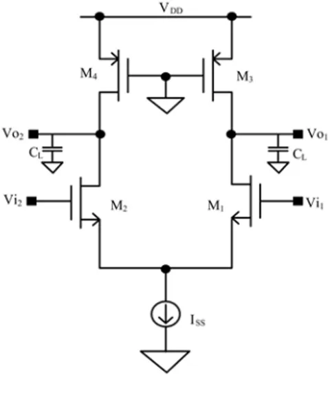
The circuit schematic of SCL inverter gate, shown in Fig. 1, is made up of an NMOS source-coupled pair having transistors working in the saturation or cut off region, that approximate well the behavior of a voltage-controlled current switch. The biasing current (Iss) is steered to one of the two output branches and converted into a differential output voltage by two PMOS transistor working in the linear region (Active load pull-up resistance)[26]. The logic function of the SCL is implemented by the logic block connected between the active load (PMOS) and the current source (Iss). For an inverter/buffer, the logic block is the differential pair constructed by NMOS transistors M1 and M2[33].
The SCL gate uses PMOS active load, but other types of load, such as physical resistor or a diode-connected NMOS/PMOS could be used. However, resistor load is not normally chosen since large silicon area needed and its parasitic capacitance can be high. For the second type of load, the output levels will loss the threshold voltage furthermore; the MOS diode load is slower than the PMOS active load for practical bias currents[34].
Fig. 1. SCL inverter
The operation of the SCL logic is based on the input differential pair circuit. The two inputs control the flow of current through the two branches of the differential pair. For example, if VGS (M2) is higher than VGS (M1), the current ID2 exceeds the current ID1. Therefore, the output voltage Vo2 begins to drop until it reach steady sate , where the current going through PMOS active load (M4) matches the ID2. In mean time Vo1 is charged to VDD through M3.
The output voltage swing Vswing is defined as voltage difference between Vo1 and Vo2 at steady state. The amount of current passing through the ON branch (M2) controls the delay of the logic gate transition (1→0), while the PMOS active load (M3) controls the charging of the output nodes (0→1 transition). Defining
∆V as the voltage drop of M3(M4) due to the drain current equal to Iss, the logic swing of the gate, Vswing equal 2∆V. To achieve best performance , all current must pass through the ON branch and the load resistance (PMOS) should be small in order to reduce the RC delay. This guarantees that the voltage is VDD - Iss.RD, where Iss is the current flowing through current source and RD is the PMOS equivalent linear resistance[33].
SCL Characteristics:
Using the standard BSIM3v3 MOSFET model[35], under the static condition, PMOS transistor can be suitably approximated by an equivalent linear resistance RD given by:
int D DS R R R 1 R int − (1)
where RDS = (RDSW 1e-6)/Wp models the source/drain parasitic resistance which depends on the empiric model parameter RDSW as well as the PMOS transistor effective channel width Wp. Rint is given by:
1 p
int eff ,p ox dd th,p p
W
R C (V | V |)
L
−
= µ −
(2)
This represent the intrinsic resistance of PMOS transistor in the linear region (it does not account for the parasitic drain/source resistance). In Eq. 2 the µeff,p represents the effective hole mobility, parameter Lp is the PMOS effective channel length, Cox is the oxide capacitance per area and Vth,p is the threshold voltage[26].
The output voltage Vo(Vi) SCL inverter can be evaluated by substituting the equivalent resistance RD in 1.
Thus, the differential output voltage Vo is equal Vo = Vo1 – Vo2 = -RD (iD1 – iD2) (3) The minimum differential input (Vi) required to fully switch the entire tail current Iss to one side is give by[36]:
2 ss
ss n ox i i n ox
1 W 2I
I C V V
W
2 L C
L
= µ →
µ
(4)
Which gives output transfer characteristics:
SS
D SS i
n ox n n
eff ,n ox n SS n
SS 2
o i D SS i
n ox n n eff ,n ox n
i SS n
SS
D SS i
n ox n n
2I
R I if v
C W L
C W
I L 2I
v (v ) vR I if | v |
C W L
C W
v
I L
2I
R I if v
C W L
〈− µ µ = − ≤ µ
µ
− 〉
µ
(5)
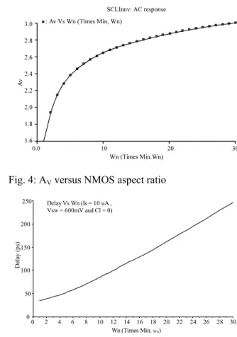
Fig. 2: Differential output voltage varying with the aspect ration of PMOS
Where, Vi = Vi1 - Vi2 (Differential input). From 5, VOL = -RD Iss and VOH = RD Iss, then the logic swing is equal to[34]:
Vswing= VOH - VOL = 2 RD Iss = 2 ∆V (6) From 5, that output voltage swing (Vswing) is a function of RD for fixed Iss. RD is controlled by the aspect ratio of PMOS, so for desired Vswing, the aspect ratio can be varied accordingly.
To verify the theoretical analysis, the simulation was carried out on the SCL inverter gate. For evaluate the Vswing, DC simulation is done by varying the aspect ratio of the PMOS with fixed Iss =10µA.
Figure 2 shows the differential output voltage of SCL inverter as function of differential input (Vi) , when (Vi) is greater certain value the SCL inverter fully switch to either side and passing all Iss to that side. The value of output voltage is function of RD and it is controlled by the aspect ratio of PMOS.
The Vswing /2 (Iss.RD) must be kept low enough to ensure the NMOS transistors M1-M2 are not in the triode region. In particular, when the gate voltage of an NMOS transistor is high (equal to VDD), the drain voltage is equal to VDD- Iss.RD, the triode region can be avoided if the gate-drain voltage VGD is lower than threshold voltage by:
GD DD DD D SS D SS th ,n
Noise Margin (NM): Due to the symmetrical property, the logic threshold is equal to zero (VLT = 0) and the associated small-signal voltage gain is gm,n.RD, (where gm,n is the small-signal transconductance of transistor M1-M2 with ID1,2 = Iss /2)[26].
Since vi1 = vi2 = vo1 = vo2 = VDD - ∆V/2 and ID1,2 = Iss /2, when the gate is biased around logic threshold, voltage VDS of transistor M1-M2 is equal to their VGS. Hence, the resulting expression of the voltage gain AV is[26]:
n
V m,n D eff ,n ox
n ss
W 1
A g R V C
L I
= = ∆ µ (8)
The NM is equal to NML (for Low-Logic) and similar to NMH (for High-Logic) due symmetrical property, which is defined as NMH = VOHmin - VIHmin (NML = VILmax - VOLmax) where VILmax and VIHmin are the input voltage values such that ∂vo/∂vi = -1. VOLmax and VOHmin are the corresponding output voltages (VOLmax = Vo(VIHmin) and VOHmin = Vo(VILmax))[34]. By differentiating (5) for vi and setting it to -1, VIHmin results is
(
2)
SS SS
IH min 2 V
n n V
eff ,n OX eff ,n OX
n n
2I I 1
V 1 8A 1
W W A
C 2 C
L L
− + +
µ µ
ss IH
n V
eff ,n ox n
2I 1
V 1
W 2A
C L
≅ −
µ
(9)
Where AV >>1/√8 has been assumed.
Approximating VOHmin to -∆V leads to the following expression of NM:
V V V
2 1 2
NM V 1 1 1
A 2A A
= ∆ − − ≅ −
(10)
Where AV >>1/√2 was assumed. The value of NM is proportional to half the logic swing[34].
Simulations were performed by setting Vswing to 600 mV, Iss to 10 uA and varying the NMOS aspect ratio (dimensions in nm). The effect of AV is shown in Fig. 3, which shows how ∂vo/∂vi changes with Wn. AV increases for low values of NMOS aspect ratio then asymptotically tends to a constant value as illustrated in Fig. 4. The SCL inverter gate output delay increases linearly as Wn increases thus limiting us to small Wn, as shown Fig. 5.
Fig. 3: Change of ∂Vo/∂Vi with different Wn
Fig. 4: AV versus NMOS aspect ratio
Delay Vs Wn (Is = 10 uA ,
Vsw = 600mV and Cl = 0)
0 50 100 150 200 250
0 2 4 6 8 10 12 14 16 18 20 22 24 26 28 30
Wn (Times Min. Wn)
De
la
y
(p
s)
Fig. 5: SCL inverter delay versus Wn
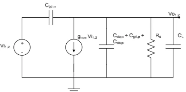
Delay analysis: To model the propagation delay,
Fig. 6: Equivalent linear half-circuit of the SCL inverter applies, since the circuit is symmetrical and it’s input is differential[25].
Figure 6, shows the small-signal model of the half-circuit concept. The half-circuit has time constant (τ) that can be evaluated by applying the open-circuit time constant method[37]. It gives the resulting delay as 0.69τ, assuming a step input waveform and neglecting the high-frequency zero. Hence, the propagation delay
τPD,SCL of the SCL gate is given by[34]:
τPD,SCL= 0.69∗RD(Cgd,n+Cdb,n+Cgd,p+Cdb,n+CL) (11) The NMOS capacitance Cgd,n, in (11) is evaluated in the saturation region. Thus its value equal to the overlap capacitance Cgd0.Weff between the gate and the drain. Junction capacitances Cdb,n and Cdb,p can be linearized by modifying their value in a zero-bias condition via coefficients Kj according to[39]. Capacitance Cgd,p is equal to the sum of the overlap contribution Cgd0Weff,p and the intrinsic contribution associated with the channel charge of the PMOS transistors working in the linear region, Cgd,p,int. In particular, we can adopt the BSIM3v3 capacitance model[36], which express capacitance Cgd,p,int as the derivative of charge flowing into drain QD with respect to the voltage VD[25]:
D
gd,p,int bulk ,max OX D
Q 3
C A WLC
V 4
∂
= ≅
∂ (12)
This derivation assumes the gate, source and bulk voltage are constant and using Abulk,max (maximum bulk charge effect) slightly greater than unity and assuming
VSD << VSG - |Vth|/Abulk.
To validate the delay model, the bias current was varied from 10-100 µA, the transistor aspect ratios were sized to obtain the typical value Vswing = 600 mV, AV = 1.94 and the load capacitance CL was set to 0 F, 100 fF and 1 pF, respectively.
SCL Delay Vs Iss with Diff. Cload
0 5000 10000 15000 20000
10 20 30 40 50 60 70 80 90 100 Iss (uA)
D
el
ay
(p
s)
Cload = 0 F Cload = 100f Cload = 1p F
Fig. 7: Delay versus bias current ISS withCL= 0, 100 fF and 1pF respectively
Fig. 8: Interconnection parastics capcitances among CMOS layers
Figure 7 show the results. As expected, the delay is decreased by increasing the bias current Iss and asymptotically tends to a constant value.
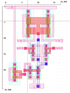
Fig. 9: 1st layout of SCL inverter
Those interconnects have an important contribution through their R and C components on the electrical circuit parameters such as delay, crosstalk or matching, especially in deep submicron technologies and that's why it becomes more important to take these effects into account during the IC simulations[40,41].
All mentioned parasitics are dependent on the way of laying out the circuit in the IC design; the way of laying out the circuit is the amount of RC parasitic is added, so, that is affecting all performance of the circuit. In the next sections different techniques of laying SCL inverter will be applied to examine the effect of RC parasitic on the output signals by employing post-simulation with input dual opposite pulses shown in Fig. 2, the limits and constrain of all layouts are the design rules of the MIMOS 0.35u PDK. First layout: Direct layout is applied and each transistor is laid as discrete component according to layout design rule. Whole W and L of NMOS/PMOS transistors are laid directly. The signal paths among different interconnections terminals are made directly as short as possible with minimum path width. Two metal layers are used M1 and M2 for signal paths. This layout utilizes 14 S/D interconnections. This layout is shown in the Fig. 9.
Second layout: Fingering technique is applied to divide the W of NMOS and PMOS on two transistors connected in parallel as shown in the Fig. 10. This layout utilizes 17 S/D interconnections and two layers M1 and M2. This layout utilizes more area than first one due of fingering.
Fig. 10: 2nd layout of the SCL inverter
0 5 10 15 19.110
0
5
10
13.760
Fig. 11: Comb layout of SCL inverter
Third layout: Comb In this layout the NMOS and PMOS transistors are laid in comb way, which reduces the area and drain/source interconnections, also its provides interdigitized and common centroide structure as shown in Fig. 11. This layout utilizes 11 S/D interconnections.
Forth layout: Fingering and Comb Both, fingering and comb techniques are applied in this time as shown in Fig. 12 and 14 S/D interconnections are used. Comparing with third layout, area is increased.
0 5 10 15 20 25.650
0
5
10
12.640
Fig. 12: Fingering and comb layout of SCL inverter
Fig. 13: Outputs of SCL inverter netlist and layouts for 100/200ns input pulses
Fig. 14: Outputs of SCL inverter netlist and layouts for 10/20ns input pulses
RC parasitic on the performance of the SCL inverter. For same inputs, the result shows that the output Vswing of the 2nd and 4th SCL inverter layout is greater than 1st and 3rd due of more interconnections of drain and source by using fingering which cause more parasitic resistance. The parasitic capacitance in 2nd layout is more than in 4th layout as more S/D interconnections are used, so more areas, which clear from switching noises. Even, the 3rd layout introduces more parasitic capacitance than 1st for the same reason. All layouts introduce some amount of resistance due of paths and
interconnections which increase the Vswing than netlist Vswing, Fig. 13, shows the outputs of SCL inverter net list and it is four layouts for input pulses of 100ns/200ns.
As the frequency of inputs pulses increases, the shape of output signals get distorted totally as the RC parasitic is function of signal frequency and the signal delay become superfluous Fig. 14.
CONCLUSION
The study work presents the basic theory and operation of SCL logic as well as the effect of layout on the SCL performance. The delay of inverter SCL gate is validated by Cadence-Spectre simulation using a 0.18µ Silterra PDK. Different parameters which affect the SCL logic are characterized. The SCL delay is decreased by increase of biasing current. The output voltage swing is small which reduce the dynamic power consumption. The SCL logic draws a fixed static current from the supply. The other advantages of SCL which inherited from its differential design include common mode noise rejection, insensitivity to process change and friendliness to neighboring analog circuit components.
The layouts introduce RC parasitic capacitance by signal paths and the way of transistor layout. The different ways of laying out the SCL inverter shows important effect on the performance and signal delay. The post-simulation shows that, the Vswing and switching noise are affected by the layout technique; also the total area of the circuit can be reduced significantly. The outputs of four different layouts of SCL show the effect of parasitics on signal delay and output resistance. The introduced parasitics by layouts are increased by increasing of inputs signal frequency. All post-simulation was carried out by using HSPICE, where the layout is done using Virtuoso - Cadence and the extraction done by using Mentor Graphic - Caliber Interactive tool on MIMOS 0.35u PDK.
REFERENCES
I. Fujimori, et al., 1997. A 5-V single chip delta-sigma audio A/D converter with 111 dB dynamic range. IEEE J. Solid-State Circuits, 32: 329-336, DOI: 10.1109/4.557630.
2. Jantzi, S.K. Martin and A. Sedra, 1997. Quadrature bandpass Sigma Delta modulator for digital radio. IEEE J. Solid-State Circuits, 32: 1935-1949, DOI: 10.1109/ISSCC.1997.585339.
4. Leopold, H.G.W., P. O'Leary, K. Ilzer and J. Jernej, 1991. A monolithic CMOS 20-b analog-to-digital converter. IEEE J. Solid-State Circuits, 26: 910-916, DOI: 10.1109/4.92009.
5. Del Signore, B.D.K., N. Sooch and E. Swanson, 1990. A monolithic 20-b delta-sigma A/D converter. IEEE J. Solid-State Circuits,
25: 1311-1317, DOI: 10.1109/ISSCC.1990.110181.
6. Allstot, D.S.C., S. Kiaei and M. Shristawa, 1993. Folded source-coupled logic vs. CMOS static logic for low-noise mixed-signal ICs. IEEE Trans. Circuits Syst. 40: 553-563, DOI: 10.1109/81.244904.
7. Su, D.M. Loinaz, S. Masui and B. Wooley, 1993. Experimental results and modeling techniques for substrate noise in mixed-signal integrated circuits. IEEE J. Solid-State Circuits, 28: 420-430, DOI: 10.1109/4.210024.
8. Masui, S., 1992. Simulation of substrate coupling in mixed-signal MOS circuits. In: IEEE Proceeding of Symposium on VLSI Circuits, 4-6 June, Seattle, WA, pp: 42-43, DOI: 10.1109/VLSIC.1992.229245.
9. Stanistic, B.N. Verghese, R. Rutenbar, L. Carley and D. Allstot, 1994. Addressing substrate coupling in mixed-mode ICs: Simulation and power distribution synthesis. IEEE J. Solid-State Circuits, 29: 226-238, DOI: 10.1109/4.278344. 10. Rabaey, J. and M. Pedram, 1996. Ed. Low Power
Design Methodologies, 1st Edition, Norwell, Kluwer, MA.
11. Lee, H.D. Hodges and P. Gray, 1984. A self-calibrating 15-bit CMOS A/D converter. IEEE J. Solid-State Circuits, 19: 813-819, URL: http://ieeexplore.ieee.org/xpl/freeabs_all.jsp?arnum ber=1052231.
12. Choy, C.C. Chan and M. Ku, 1995. A feedback control circuit design technique to suppress power noise in high speed output driver. In: IEEE Proceeding of International Symposium on Circuits and Systems, ISCAS'95, 28 April - 3 May, Seattle, WA, Vol.1, pp: 307-310, DOI: 10.1109/ISCAS.1995.521512.
13. Choy, C. C. Chan, M. Ku and J. Povazanec, 1997. Design procedure of low-noise high-speed adaptive output drivers. In: IEEE Proceedings of International Symposium on Circuits and Systems, ISCAS'97, 9-12 June, Hong Kong, Vol.3, pp: 1796-1799, DOI: 10.1109/ISCAS.1997.621494.
14. Takaramoto, T.S. Harajiri, M. Sawada, O. Kobayashi and K. Gotoh, 1991. A bonded-SOI-wafer CMOS 16-bit 50-KSPS delta-sigma ADC. In: IEEE Proceedings of Custom Integrated Circuits Conference, 12-15 May, San Diego, CA,
pp: 18.1/1-18.1/4, DOI: 10.1109/CICC.1991.164100.
15. Kiaei, S.S. Chee and D. Allstot, 1990. CMOS source-coupled logic for mixed-mode VLSI. In: IEEE Proceeding of International Symposium on Circuits Systems, 1-3 May, New Orleans, LA, vol.2, pp: 1608-1611, DOI: 10.1109/ISCAS.1990.112444.
16. Kiaei, S. and D. Allstot, 1992. Low-noise logic for mixed-mode VLSI circuits. Microelectron. J., 23: 103-114, DOI: 10.1016/0026-2692(92)90042-Y 17. Maskai, S. S. Kiaei and D. Allstot, 1992. Synthesis
techniques for CMOS folded source-coupled logic circuits. IEEE J. Solid-State Circuits, 27: 157-1167, DOI: 10.1109/4.148324.
18. Sàez, R.M. Kayal, M. Declercq and M. Schneider, 1996. Digital circuit techniques for mixed analog/digital circuits applications. In: IEEE Proceedings of the Third IEEE International Electronics, Circuits, and Systems, ICECS '96, Rodos, Greece, Vol.2, pp: 956 – 959, DOI: 10.1109/ICECS.1996.584544.
19. Senthinatan, R. and J. Prince, 1993. Application specific CMOS output driver circuit design techniques to reduce simultaneous switching noise. IEEE J. Solid-State Circuits, 28: 1383-1388, DOI: 10.1109/4.262016.
20. Kundan, J. and S. Hasan, 1997.Current mode BiCMOS folded source-coupled logic circuits. In: IEEE Proceedings of International Symposium Circuits and Systems, ISCAS '97, 9-12 June, Hong Kong, Vol.3, pp: 1880-1883, DOI: 10.1109/ISCAS.1997.621516.
21. Saez, R., M. Kayal, M. Declercq and M. Schneider, 1997. Design guidelines for CMOS current steering logic. In: IEEE Proceedings of International Symposium on Circuits and Systems, ISCAS'97, 9-12 June, Hong Kong, Vol.3, pp: 1872-1875, DOI: 10.1109/ISCAS.1997.621514. 22. Ng, H. and D. Allstot, 1997. CMOS current
steering logic for low-voltage mixed-signal integrated circuits. IEEE Trans. VLSI Syst., 5: 301-308, DOI: 10.1109/92.609873.
24. Rabaey, J. and M. Pedram, 1996. Low Power Design Methodologies, 1st Edition, Norwell. Kluwer, MA.
25. Alioto, M.G. Palumbo and S. Pennisi, 2002. Modeling of source coupled logic gates. Int. J. Circuit Theor. Appl., 30: 459-477, DOI: 10.1002/cta.188.
26. Alioto, M. and G. Palumbo, 2003. Design strategies for source coupled logic gates. IEEE Trans. Circuits Syst., 50: 640-654, DOI: 10.1109/TCSI.2003.811023.
27. Wilson, G.R., 1990. Advances in bipolar VLSI. Proc. IEEE, 78: 1707-1719, DOI: 10.1109/5.63299. 28. Treadway, R.L., 1989. DC analysis of current
mode logic. IEEE Circuits Devices Mag., 5: 21-35, DOI: 10.1109/101.19320.
29. Ng, P.T. Balsara and D. Steiss, 1997. Performance of CMOS differential circuits. IEEE J. Solid-State Circuits, 31: 841-846, DOI: 10.1109/4.509871. 30. Greub, H.J., J.F. Mcdonald, T. Creedon and
T. Yamaguchi, 1991. High-performance standard cell library and modeling technique for differential advanced bipolar current tree logic. IEEE J. Solid-State Circuits, 26: 749-762, DOI: 10.1109/4.78245. 31. Razavi, B.Y. Ota and R. Swartz, 1994. Design
techniques for low-voltage high speed digital bipolar circuits. IEEE J. Solid-State Circuits, 29: 332-339, DOI: 10.1109/4.278358.
32. John, P. Uyemura, 2001. CMOS Logic Circuit Design.1st Edition, Dordrecht: Kluwer Academic Puplisher .
33. Mohamed, W. Allam and Mohamed I. Elmasry, 2001. Dynamic Current Mode Logic (DyCML): A new low-power high-performance logic style. IEEE J. Solid-State Circuits, 36: 550 – 558, DOI: 10.1109/4.910495.
34. Massimo, A. and G. Palumbo, 2005. Model and Design of Bipolar and MOS Current-Mode Logic: CML, ECL and SCL Design Circuit. 1st edition, Dordrecht, Springer.
35. Cheng, Y. and C. Hu., 1999. MOSFET Modeling and BSIM3 User's Guide. 1st edition, Boston, Kluwer, MA .
36. Michael, M. Green and Ullas Singh, 2003. Design of CMOS CML circuits for high-speed broadband communication. In: IEEE Proceeding of International Circuits and Systems symposium, ISCAC’03, 25-28 May, Bangkok, Thailand, 2:
204-207, URL: http://ieeexplore.ieee.org/xpl/freeabs_all.jsp?arnum
ber=1205937.
37. Cochrun, B. and A. Grabel, 1973. A method for the determination of the transfer function of electronic circuit. IEEE Transact. Circuit Theor., 20: 16-20, URL:
http://ieeexplore.ieee.org/xpl/freeabs_all.jsp?arnum ber=1083615.
38. Rabaey, J., 1996. Digital Integrated Circuit A Design Prospective. 1st edition, Englewood Cliffs, Prentice-Hall, NJ.
39. Albina, C.M. and G. Hackl, 2006. Layout parasitic limitations in high-speed circuits. Int. Semiconductor Conf., 2: 375-378, DOI: 10.1109/SMICND.2006.284023.
40. Jason, D.Z., P. Cong and P.V. Srinivas, 2001. Improved crosstalk modelling with applications to noise constrained interconnect optimization. In: Proceedings of the Asia and South Pacific Design Automation Conference (ASP-DAC), ASP-DAC 2001, Yokohama, Japan, Jan-Feb., pp: 373-378, DOI: 10.1109/ASPDAC.2001.913335.