Brazilian Journal of Physics, vol. 36, no. 2A, June, 2006 361
Growth and Structural Characterization of PbTe/PbEuTe Double Barrier
A. M. P. dos Anjos, E. Abramof, and P. H. O. Rappl
Laborat´orio Associado de Sensores e Materiais, Instituto Nacional de Pesquisas Espaciais, Caixa Postal 515, 12245-970, S˜ao Jos´e dos Campos-SP, Brazil
Received on 4 April, 2005
A series of PbTe/PbEuTe double barrier samples with different barrier widths were successfully grown on BaF2substrates by molecular beam epitaxy. The electron concentration of PbTe spacer and well layers was
controlled by the deviation from stoichiometry, while the buffer and cap layers were intentionally doped with bismuth to obtain low-resistivity layers to be used as top and bottom contacts. Assuming 50% of band offset, a barrier height of 150 meV was determined by infrared transmission measurements, corresponding to a PbEuTe barrier with 5% of europium content. The structural parameters of the samples were accurately determined by combining the measurement in a high-resolution x-ray diffractometer in the triple-axis configuration with a simulation within the framework of dynamical theory of diffraction.
Keywords: PbTe/PbEuTe double barrier; BaF2substrates; Molecular beam epitaxy
I. INTRODUCTION
Molecular beam epitaxy (MBE) has been successfully ap-plied for the growth of PbEuTe/PbTe heterostructures. New interesting research possibilities were opened by alloying the binary and also ternary lead salts with rare-earth elements to produce compounds with higher energy gaps and their respec-tive multi-layer heterostructures [1-5]. Usually, PbTe is used for the quantum wells and ternary Pb1−xEuxTe with x≤0.05 for the barriers. The advantage of using Pb1−xEuxTe in lead salt heterostructures is the pronounced increase of the energy band gap with Eu content. For instance, Pb1−xEuxTe with x = 0.06 (Eg = 530 meV at 295 K) yields a barrier of 110 meV, considering a band offset of 50% [4,5].
Transport measurements in PbTe/PbEuTe structures have led to interesting results like weak electron localization in Pb1−xEuxTe layers at low temperature [6], observation of the integral quantum Hall effect in PbTe/Pb1−xEuxTe multi-quantum wells [7], and conductance quantization in small constrictions in PbTe layers [8]. All these transport measure-ments have been performed with current flowing in the sample plane. To our knowledge, no publication in the literature deals with vertical transport (charge flowing parallel to the growth direction) in IV-VI compounds. The objective of this paper is to grow and characterize the structure of PbTe/PbEuTe double barrier samples. These devices are designed to the measure-ment of resonant tunnelling.
Here, we report on the growth of a series of PbTe/PbEuTe double barrier (DB) samples on BaF2substrates, using a MBE system dedicated to the IV-VI compounds and related eu-ropium alloys. The Eu content of the barriers was determined by infrared transmission [5] on reference Pb1−xEuxTe layers. The electrical characteristics of these layers were obtained by Hall effect measurements. In order to determine the structural parameters of the DB’s, the x-ray spectra of all samples were measured in a high-resolution diffractometer in the triple-axis configuration.
II. EXPERIMENTAL AND RESULTS
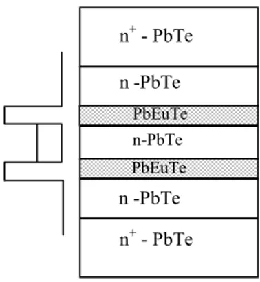
The layer sequence of the PbTe/PbEuTe double barrier structures, which we intend to grow here, is shown in Fig. 1. The structure is composed of an n+-PbTe buffer layer (∼3µm) grown on top of a BaF2substrate, followed by a 14 nm n-PbTe spacer layer, the double barrier itself (PbTe well sandwiched between two PbEuTe barriers), another 14 nm n-PbTe spacer, plus a 45 nm n+-PbTe cap layer. The n+-PbTe bottom and top layers are to optimize electrical contacts.
All samples were grown on freshly cleaved (111) BaF2in a Riber 32P MBE system equipped with effusion cells contain-ing solid sources of PbTe, Te(1), Eu, Te(2) and Bi2Te3. The first tellurium effusion cell is used to control the stoichiometry of the PbTe layers, while the second one to balance the beam fluxes during the growth of PbEuTe layers. To achieve elec-tron concentration higher than 1017 cm−3, it is necessary to dope PbTe extrinsically through the Bi2Te3cell. In a previous work [9], we demonstrated the successful n-type doping of PbTe layers with well-controlled doping levels ranging from 1017to 1020cm−3.
n+ - PbTe
n -PbTe
n-PbTe PbEuTe
PbEuTe
n -PbTe
n+ - PbTe
FIG. 1: Layer sequence of a PbTe/PbEuTe double barrier structure.
struc-362 A.M.P. dos Anjos et al.
ture. During this experiment, the PbTe effusion cell temper-ature was kept fixed at 647 ˚ C, and the layers were always deposited at a substrate temperature of 300oC. In these condi-tions the growth rate was about 2 ˚A/s.
The temperature of the Te(1) effusion cell was adjusted to control the stoichiometry deviation and obtain an n-type PbTe layer with an electron concentration close to 1x1017 cm−3. The bismuth telluride beam flux was set to achieve an n+ -PbTe layer with electron concentration in the range of high 1019cm−3. To determine the electrical properties of the refer-ence layers, Van der Pauw geometry samples were prepared by soldering Au wires with In pellets. The measurements were performed at 300 and 77K in a Keithley Hall effect sys-tem with a magnetic field of 7000 Gauss, and the results are summarized in Table 1. To obtain these layers, the Te(1) and Bi2Te3effusion cell temperature was set to 275 and 460 ˚ C, respectively.
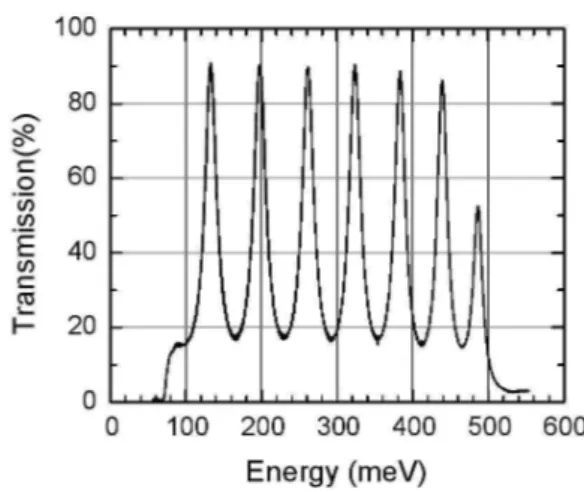
Note that the bismuth addition to the n-PbTe layer increases the concentration from 1.4x10¹⁷to 9x1019 cm−3at 77K and decrease the resistivity from 1.8x10⁻² to 1.3x10⁻⁴ Ω cm. The n+-PbTe layer is then appropriated for the top and bot-tom contacts in the DB samples. The carrier mobilities are naturally reduced due to the increase in carrier concentration. The europium content of the Pb1−xEuxTe barrier was con-trolled by the Eu effusion cell temperature and the Te(2) beam flux is adjusted to maintain a Te/Eu beam flux ratio of 2 dur-ing growth. To determine the Eu content, the energy gap of Pb1−xEuxTe reference layers was obtained from infrared transmission spectrum [4,5]. The measurements were per-formed at 300K in a Perkin Elmer FTIR 1600 Fourier trans-form spectrometer in a frequency range from 500 to about 4500 cm−1 (55 to about 550meV). Fig. 2 shows the trans-mission spectrum of a Pb1−xEuxTe reference layer grown on a BaF2substrate with Eu and Te(2) effusion cell temperature of 335 and 300 ˚ C, respectively. The energy gap is determined by the cut-off energy at the right-hand side of the spectrum. The Eu content x is then obtained by the following expression [5], which relates the energy gap at 300K to the Eu content for Pb1−xEuxTe layers.
Eg(meV) =321+3487.32x
The Eu content calculated for the reference layer in Fig. 2 was x = 0.05. This energy gap leads to a potential barrier of 150 meV for PbTe in the DB structure in both conduction and valence bands, assuming 50% for the band offsets. The electrical properties of this p-type Pb1−xEuxTe reference layer are also shown in Table 1.
After the calibration procedure for the individual layers, the remote MBE shutter control was programmed to obtain the desired double barrier structure. For this series, we decided to vary the PbEuTe barrier thickness, but still keep it below the critical value, in order to maintain the whole DB structure co-herent, i.e., with the same in-plane lattice parameter of PbTe. The critical thickness of Pb1−xEuxTe with x∼0.05 on top of PbTe was evaluated from the simple relation tc=1/ f (in mono-layers) [10], where f is the lattice misfit between both layers. Using 6.460 and 6.473 ˚A for PbTe and Pb0.95Eu0.05Te lattice
FIG. 2: Infrared transmission spectrum of a Pb1−xEuxTe reference layer. The energy gap is determined by the cut-off at the right side.
constants, respectively, we get a critical thickness of about 180 nm. Considering this top limit, we varied the growth time of PbEuTe from 15 to 400s in our series, keeping the time of 25s for the growth of PbTe well.
In situ RHEED at 12keV was performed in order to evalu-ate the surface and interface quality of the films during epitax-ial deposition. The RHEED transitions from islands to layer-by-layer growth mode occurred at about 50 nm of growth. For the heteroestructure on top of n-PbTe buffer, the RHEED pat-tern remained totally streaked during the entire double barrier growth process, indicating the persistence of a smooth surface throughout the stack.
In order to determine the structural parameters of the PbTe/PbEuTe double barrier, the x-ray spectra of all sam-ples were measured in a high-resolution diffractometer in the triple-axis configuration. Our Philips X’Pert diffractometer was configured with a four-crystal Ge(220) monochromator in the primary optics (between the Cu x-ray tube and the sam-ple) and a Ge(220) channel-cut analyzer immediately before the detector to increase substantially the resolution in the 2θ direction.
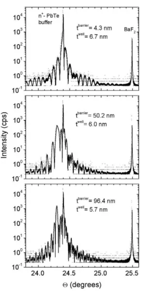
Figure 3 shows theω/2θscan around the (222) Bragg dif-fraction peak for three PbTe/PbEuTe DB samples with differ-ent barrier thickness. The spectra shows the n+-PbTe buffer layer as the most intense peak, the BaF2substrate peak, which was used as a reference for theΘscale, and the interference pattern form the DB structure itself. Note that the intensity of the diffraction pattern due to the DB structure is two to four orders of magnitude lower than that of the PbTe buffer layer. For this reason, we had to use a large integration time (5s) for each angular step. Observe also that, as the barrier width increases, the most intense peak of the DB diffraction pattern moves to lower angles away from the PbTe buffer peak, and increases in intensity.
Brazilian Journal of Physics, vol. 36, no. 2A, June, 2006 363
TABLE I: Resistivity (ρ), Hall mobility (µ)and carrier concentration (n/p)for individual layers at 77 and 300K.
Layer T
(K)
ρ
(Ωcm)
µ (cm2/Vs)
n/p (cm−3)
n-PbTe 77 1.86 x 10⁻² 23100 1.45x10¹⁷
300 1.01x10⁻¹ 459 1.33x10¹⁷
n+-PbTe 77 1.34x10⁻⁴ 514 9.02x10¹⁹
300 3.94x10⁻⁴ 195 8.10x10¹⁹
p-Pb1−xEuxTe 77 1.72 x10⁻¹ 113 3.18x10¹⁷
x=0.05 300 3.51x10⁻¹ 38 4.61 x10¹⁷
FIG. 3:ω/2Θscans around the (222) Bragg diffraction peak of three PbTe/PbEuTe double barrier samples, with different barrier thick-nesses, grown on BaF2substrates.
TABLE II: Double barrier structural parameters obtained from the x-ray analysis: lattice parameter (a) of PbTe and PbEuTe and thickness (t) of the well (W), barrier (B), spacer (S), and cap (C) layers.
Sample a ( ˚A) t ( ˚A)
PbTe PbEuTe W B S C
4050 6.4600 6.4741 60 45 144 432 4019 6.4603 6.4743 67 43 162 486 4100 6.4608 6.4750 57 242 138 414 4099 6.4607 6.4735 60 502 144 432 4098 6.4600 6.4734 57 964 138 414
[3,11] and compared to the measuredω/2θscans.
For the simulation, we take the sample structure shown in Fig. 1 and assumed that the PbEuTe barriers are completely strained to the PbTe layer, which is confirmed by the bell shape of the diffraction pattern. First of all, the lattice con-stant of PbTe is adjusted to fit both PbTe buffer and BaF2 (a=6.2000 ˚A) substrate peaks. The value found for the PbTe lattice constant for each sample is shown in Table 2. A mean value of 6.4604 ˚A is encountered. In the fitting program, the thickness of each individual layer was calculated by the growth rate multiplied by the respective MBE shutter open-ing time. The PbEuTe growth rate was considered to be (1+x) times the PbTe growth rate. In this manner, the PbTe growth rate and the PbEuTe lattice constant remained as the main fit-ting parameters. The values found for the PbEuTe relaxed lattice constant are also shown in Table 2.
364 A.M.P. dos Anjos et al.
III. CONCLUSION
We have successfully produced a series of PbTe/PbEuTe double barrier structures, with different barrier thickness, grown on BaF2substrates by molecular beam epitaxy. The electron concentration of the PbTe spacer and well layers was controlled by the deviation from stoichiometry, while the buffer and cap layer were intentionally doped with bismuth to obtain low-resistivity layers to be used as top and bottom contacts. It was possible to have a good control on the eu-ropium content of the PbEuTe layers. A value of x=0.05 was
chosen for this series. The x-ray analysis allowed an accurate determination of the structural parameters, and the agreement between the measured and calculated x-ray spectra indicated that coherent double barrier structures with sharp interfaces were obtained.
Acknowledgement
We are grateful to partial support of FAPESP (Grant Nr. 00/12529-6) and CAPES (scholarship of first author).
[1] G. Springholz and G. Bauer, J. Cryst. Growth 144, 157 (1994). [2] D. L. Partin, IEEE J. Quantum Electron. QE-24, 1716 (1988). [3] E. Abramof, P. H. O. Rappl, A. Y. Ueta, and P. Motisuke, J.
Appl. Phys. 88, 725 (2000).
[4] E. Abramof, E. A. de Andrada e Silva, S. O. Ferreira, P. Mo-tisuke, P. H. O. Rappl, and A. Y. Ueta, Phys. Rev. B 63, 085304 (2001).
[5] S. Yuan, H. Krenn, G. Springholz, A. Y. Ueta, G. Bauer, and P. J. McCann, Phys. Rev. B. 55, 4607 (1997).
[6] A. Prinz, G. Brunthaler, A. Y. Ueta, G. Springholz, G. Bauer, G. Grabecki, and T. Dietl, Phys. Rev. B 59, 12983 (1999). [7] G. Sprinholz, G. Ihninger, G. Bauer, M. M. Olver, J. Z.
Pasta-lan, S. Romaine, and B. B. Goldberg, Appl. Phys. Lett. 63, 21 (1993).
[8] G. Grabecki, J. Wr´obel, T. Dietl, K. Byczuk, E. Papis, E. Kaminska, A. Piotrowska, G. Spingholz, M. Pinczolits, and G. Bauer, Phys. Rev. B 60, R5133 (1999).
[9] A. M. P. dos Anjos, E. Abramof, P. H. O. Rappl, A. Y. Ueta, and H. Closs, Braz. J. Phys. 34, 653 (2004).
[10] D. J. Dunstan, S. Young, and R. H. Dixon, J. Appl. Phys. 70, 3038 (1991)