Abstract— This article presents the design of K-band Substrate
Integrated Waveguide (SIW) Band-pass filter with high rejection, by using the topology with iris and the SIW resonators. The simulated results of this filter have shown that the passband is from 17.3 GHz to 19.3 GHz, while the insertion loss is 1.35 dB within 10.9 % bandwidth around 18.3 GHz and input return loss in the passband is better than 15 dB, with high rejection of -57.88 dB at the frequency 24.07 GH. All the structures are designed on a single substrate of Rogers R04003 permittivity 3.55. The compatibility with planar circuits is provided via a specific microstrip transition (microstrip tapered transitions).
Index Terms— SIW cavity resonator, microwave filters, transition,
SIW-microstrip technology.
I. INTRODUCTION
A High selectivity, low insertion loss, small size and limited cost are so many essential questions in
the design and the manufacturing of microwave circuits. Unfortunately, the traditional technology,
either planar or non-planar, is incapable to provide all these characteristics at the same time. In fact,
the rectangular waveguides present low insertion losses and good selectivity. However, their
production is costly and their integration with other planar circuits requires a specific transition. For
planar circuits have a low quality factor, but they have a good compatibility and low cost
manufacturing. These constraints led us to use the SIW technology to combine the respective
advantages of the technologies previously mentioned.
The SIW concept associates the use of planar technology microstrip and the functioning of cavities
in which are going to exist volume modes. Technically, cavities are included in the substratum and are
delimited for the upper and lower faces by the metal plane and for the side faces by rows of metallic
holes. This vias have a diameter and spacing small to appear as electric walls [1]-[10].
The SIW (Substrate Integrated Waveguide) structures have been of great interest and with a specific
transition that this technology is compatible with some planar technologies [11], [12]. The SIW has
been applied successfully to the conception of planar compact components for the microwave and
Design of K-Band Substrate Integrated
Waveguide Band-Pass Filter with High
Rejection
Ahmed Rhbanou, Mohamed Sabbane
Department of Mathematics, FSM, Moulay Ismail University, Meknes, 50000, Morocco
E-mail:[email protected] Seddik Bri
millimeter wave applications. Such as filters [13]-[17].
In this paper, the properties of the SIW bandpass filter in the K-band with iris topology are carefully
studied in their equivalent circuit and their design. Then the equivalent circuit of SIW bandpass filter
with high rejection was studied using the rules and conventional synthesis tools to define the coupling
matrix of this filter. After defining the equivalent circuit, the second phase will be the study of the
design, but before an important part will be devoted to resonators SIW, for produce the bandstop. The
use of resonators and SIW bandpass filter allows the design of a filter having the peculiarity of
offering a very high rejection located and close to the bandwidth. The simulations of the equivalent
circuits were made by the method of moments (MoM) based on commercial software package (ADS).
On the other hand the simulations of the structures were made by the finite element method (FEM)
based on a commercial software package (HFSS). The results obtained by HFSS simulation are
compared and discussed with the results in [18].
II. DESIGN OF THE CAVITY RESONATOR SIW AND QUALITY FACTOR
The propagation properties in the SIW and in the conventional metallic rectangular waveguide are
very similar. In particular, the electromagnetic field distribution is TE101 [1], Thus, the initial
dimensions of the SIW resonator cavity can be determined by the conventional resonant frequency
formula of metallic waveguide resonator (fc101), where the length and width of the metallic cavity, Leff
and Weff, should be replaced by the equivalent width WSIW and length LSIW of the SIW cavity because
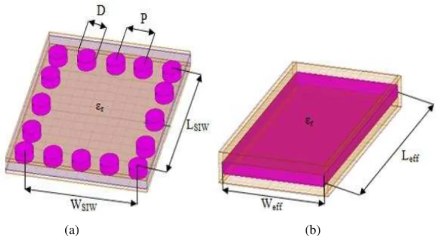
of the presence of vias sidewall as shown in Fig. 1.
(a) (b)
Fig. 1. (a) Cavity resonator SIW. (b) Rectangular cavity waveguide filled with dielectric.
A SIW cavity can be designed by using the relations 1, 2 and 3 provided that P < λ0*( r/2) 1/2
and P < 4*D with r relative permittivity, D and P are the diameter of the metallic via and the period
of via holes respectively [2]-[9].
2 2
1 1
2
1 0 1
L
W
f
eff eff r cc
(1)P
D
W
W
eff SIWP
D
L
L
eff SIW95 . 0 2 (3)
The quality factor (Qpr) of a SIW cavity is presented by the following equation 4 [10]:
Q
Q
Q
pr d c1 1 1
(4)
With (Qd) resulting from the power loss in the lossy dielectric material filling the cavity and (Qc)
resulting from the power loss in the walls which have finite conductivity.
tan
1
Q
d (5)F
s r c
Q
(6)Where (tan ) is the loss tangent of the dielectric, (λr) is the free-space wavelength in the dielectric
to the cavity resonant frequency and ( s) is called the skin depth. (F) is the shape factor of the SIW
cavity, for resonance in TE101 mode, the expression of (F) is given by equation 7.
L
h
W
L
W
W
h
W
L
W
SIW SIW SIW SIW SIW SIW h SIW h SIW h F 2 2 2 2 2 2 2 2 / 31
1
(7)The parameters WSIW, LSIW and h are respectively the width, the length and the height of the SIW
cavity.
III. THEORETICAL STUDY OF BAND PASS FILTER AND PROPOSED TRANSITIONS
Generally, the microstrip transitions are very required to combine SIW and microstrip technologies.
Tapered transition shown in Fig. 2 has been studied. This kind of transition consists of a tapered
microstrip line section that connects a 50 microstrip line and the integrated waveguide. The physical
characteristics of microstrip line (the width WM) and the dimensions (width WT and length LT) of a
transition are widely detailed in [11], [12].
Fig. 2. SIW Guide with tapered transitions.
The microwave band-pass filters are presented by an equivalent circuit [13]. This circuit consists of
impedance inverters and parallel resonant circuits. The number of the resonators or the order of the
filter (N) is determined by equation 8 applicable in the case of Chebyshev synthesis [13]. With LAs is
frequency [13], whose cut-off frequency is Ωc=1 rad/s.
S
L L N
Ar As
cosh
10
10
cosh
1 1 . 0
1 . 0 1
1 1
(8)
The resonators in equivalent circuit are modeled by inductance and capacitance in series [13]. The
coupling coefficients between resonators are provided by impedance inverters Ki,i+1(0≤ i ≤n) [13], so
the filter coupling matrix is presented in following form:
Fig. 3. Coupling matrix of the microwave bandpass filter circuit.
The indices S and L correspond to the source and to the load respectively, in other words to the
accesses. The indices going from 1 to n correspond to the resonators.
On the other the waveguide filters are formed with resonator distributed elements interconnected by
impedance inverters or admittance. The equivalent circuit of the band-pass filter SIW is presented by
impedance inverter and phase shifts [14]. The impedance inverters Ki,i+1(0≤ i ≤n) are given by the
formulas in [15].
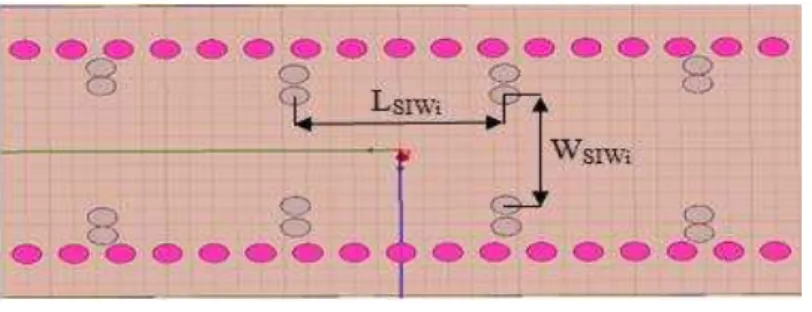
The SIW filter with iris is influenced by the lengths LSIWi(i=1,2,3…,n) the resonators and also by
the coupling, That is an opening in the wall between two adjacent cavities. This type of opening is
called iris (the widths WSIWi (i=0,1,2…..n) the resonators), as illustrated in Fig. 4.
Fig. 4. SIW filter with iris.
The widths WSIWi (i=0,1,2…..n) of the resonators in SIW technology are determined by the abacus
of the estimated width in rectangular waveguide [16]. The lengths LSIWi (i=1,2,3,…n) the resonators
IV. RESULTS
A. SIW filter with inductive post-wall irises in the K-band
In this work, all the structures are designed on a single substrate of Rogers R04003 permittivity r
=3.55 and height h = 0.508 mm.
Generally to determine the parameters of SIW guide, designed in the K-band [15-22] GHz from a
conventional wave guide with dimensions a= 12.954 mm and b= 6.477 mm, using the formulas given
by equations 1, 2 and 3 for mode TE10. With the diameter of the metallic via D = 0.5 mm and the
period of the vias P =1 mm. Following this approach, the distance between the rows of the centres of
via is WSIW =7.13 mm and the length of SIW guide is LSIW =Leff =80 mm because does not bring
significant change in the propagation phenomenon.
A microstrip transition (taper) is used to interconnect SIW to the planar transmission lines. There is
a tapered section which is used to match the impedance between a 50 Ω microstrip line and the SIW.
The 50 Ω microstrip line, in which the dominant mode is quasi-TEM, can excite well the dominant
mode TE10 of the SIW, as their electric field distributions are approximate in the profile of the
structure.
The dimensions of the transition and the microstrip line are WM=1.13, WT =2.4 mm and LT =14.565
mm. A schematic view of a SIW with two tapered transitions is shown in Fig. 5.
Fig. 5. SIW with two tapered transitions.
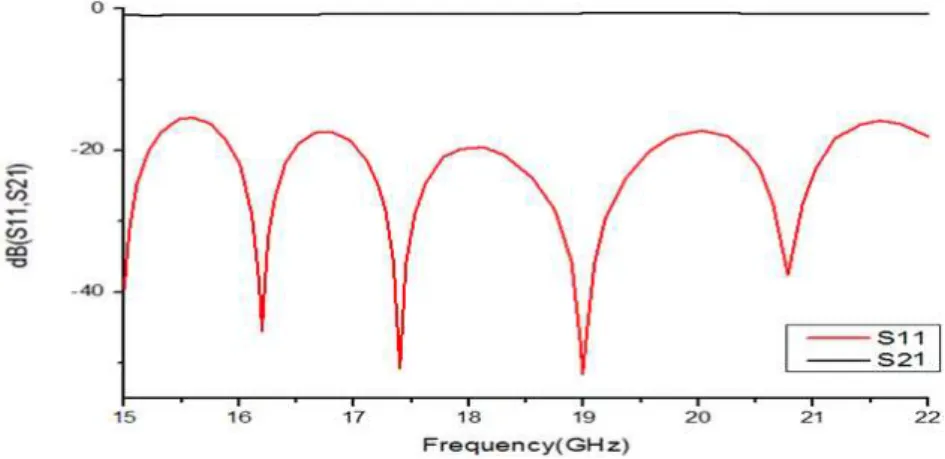
This structure is simulated by using HFSS. The simulated S-parameters of SIW with two tapered
transitions in the frequency band [15-22] GHz are shown in Fig. 6.
Fig. 6. Frequency response of SIW with two tapered transitions.
The results illustrated in Fig. 6, indicate that the reflection coefficient S11 remains below -15 dB
across the entire band and the transmission coefficient S21 is around 0.8 dB.
using software 2D simulation (ADS). This filter has a centre frequency f0= 18.35 GHz, the absolute
bandwidth 2 GHz and the relative bandwidth FBW = 10.9 %, the ripple is 0.01 dB. The filter must
submit a rejection of -20 dB at 20.8 GHz. Therefore, a 4rd degree SIW filter, the circuit model of
microwave filter in ADS is shown in Fig. 7.
Fig. 7. Circuit model of microwave filter in ADS.
K0.1 and K4.5 correspond to access coupling coefficients, K1.2, K2.3 and K3.4 correspond the coupling
coefficients between resonators. The function tuning of ADS is used to enable adjustment of the
coupling coefficients Ki,i+1 (0≤ i ≤4). Finally, the coupling matrix is shown in Fig. 8.
Fig. 8. Coupling matrix of the microwave bandpass filter circuit.
The indices S and L correspond to the source and to the load respectively, in other words to the
accesses. The indices going from 1 to 4 correspond to the four resonators. The ideal frequency
response circuit in the K-band is shown in Fig. 9.
Fig. 9. Ideal frequency response of the model circuit in ADS.
The result simulated by ADS in Fig. 9, shows that the full frequency passband is from 17.3 to 19.3
GHz. the center frequency f0= 18.3 GHz, the absolute bandwidth 2 GHz and the relative bandwidth
FBW= 10.9 %. The return loss is better than 20 dB between 17.64 GHz and 18.98 GHz. You can be
seen that the filter respects well the tender specifications.
the Rogers R04003 substrate for comparing with the results in [18]. The structure of SIW bandpass
filter in the K-band with iris topology a 4rd order is shown in Fig. 10.
Fig. 10. SIW filter with stepped transition using post-wall irises.
Using the method of the abacus, to find the results which are going to be optimized by HFSS, the
final dimensions of the structure are: LSIW1=LSIW4=4.43 mm, LSIW2=LSIW3=5.17 mm, WSIW0=WSIW4=4.4
mm, WSIW1=WSIW3=3.2 mm, W SIW2=2.94, WT=2.4 mm, LT=14.565 mm, D = 0.5 mm, P =1 mm, WSIW
= 7.13 mm, WM =1.13 mm. Fig. 11 illustrated the reflection coefficient S11 and the transmission
coefficient S21 of SIW bandpass filter in the K-band with iris and also the results in [18].
(a)
(b)
The result simulated by HFSS shows that the full frequency passband is from 17.3 to 19.2 GHz. the
center frequency f0= 18.25 GHz, the absolute bandwidth 1.9 GHz and the relative bandwidth
FBW= 10.4 %. The insertion loss around 18.25 GHz is approximately 1.3 dB, the return loss in the
passband is better than 20 dB between 17.56 GHz and 18.87 GHz.
On the other side, the result simulated by HFSS in [18] shows that the full frequency passband is
from 17.3 to 19.3 GHz. the center frequency f0= 18.3 GHz, the absolute bandwidth 2 GHz and the
relative bandwidth FBW= 10.9 %. The insertion loss around 18.3 GHz is approximately 1.3 dB, the
return loss in the passband is 10 dB, with high rejection of -57.88 dB at the frequency 24.07 GHz.
Both results are in good agreement, but the result simulated by HFSS in [18] shows a high
rejection, because of the use of resonators SIW.
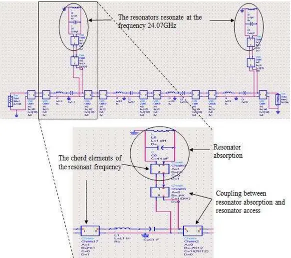
B. Equivalent circuit SIW bandpass filter in the K-band with high rejection
The equivalent circuit of SIW filter in the K-band is realized (Fig. 7). For to have an rejection in
24.07 GHz, using the same (LC) resonators as the other resonators, which model the absorption
cavities dimensioned to resonate at frequencies to reject (24.07 GHz) and added to the filter, the
frequencies to be rejected are adjusted using the chord elements that model a parallel reactance.
Moreover, each resonator receives a parallel reactance, to adjust their resonant frequency after adding
the absorption resonators. Modeling circuit of this modification, with the addition of a resonator in
Fig. 12. Circuit model of SIW filter with resonators absorption.
The ADS tuning tool will be called upon to adjust the various settings that are the coupling
coefficients and the parallel reactors, for obtain the coupling matrix shown in Fig. 13.
Fig. 13. Coupling matrix of the microwave bandpass filter circuit integrating absorption resonators.
BSRC1 and BSRC2 correspond to the two resonators absorption (Band-Stop Resonator Cavity),
they resonate at the frequency of 24.07 GHz, the diagonal elements corresponding to the absorption
Fig. 14. Frequency response of the circuit model.
The result simulated by ADS in Fig. 14, shows that the full frequency passband is from 17.3 GHz to
19.3 GHz. the center frequency f0=18.3 GHz, the absolute bandwidth 2 GHz and the relative
bandwidth FBW= 10.9 %. The return loss is better than 15 dB between 17.61 GHz and 18.86 GHz,
with high rejection of -68 dB at the frequency 24 GHz.
C. Configuration of the resonators SIW
The design of a filter having the peculiarity to offer a very high rejection located and close to the
bandwidth, needs to use the resonators for to produce the bandstop response.
A square cavity (Weff =Leff) in TE101 mode, allows it away to the parasitic modes in the spectrum.
The width and the length of the cavity resonator SIW are WSIW=LSIW=4.7 mm, with the dimensions of
the transition and the microstrip line are: WM=1.13, WT =2.4 mm and LT =14.565 mm, the quality
factor (Qpr) of this cavity resonator SIW is 370.
The structure and the dimensions of the cavity resonator SIW with two tapered transitions are
shown in Fig. 15.
Fig. 15. Resonator SIW with two tapered transitions.
The transmission coefficient S21 and the reflection coefficient S11 of the cavity resonator SIW with
Fig. 16. Frequency response of resonator SIW with two tapered transitions.
The simulation of the resonator SIW in Fig. 16 showed that the resonance frequency was at 23.12
GHz. After studying the cavity resonator SIW bandpass, passing the bandstop response, by using a
SIW guide connects to the cavity resonator SIW (Fig. 17).
Fig. 17. Configuration of cavity resonator SIW bandstop with two tapered transitions.
Where (B) and (A) are the width and the length of SIW cavity that affects the bandstop response,
the value (C) is the input length of resonator. To reach the 24.07 GHz by varying the width of the
cavity while the rest of the dimensions are being kept constant.
The transmission coefficient S21 of resonator SIW bandstop is shown in Fig. 18, for the values of
the width (B) equal to 4.7 mm, 3.435 mm and 2.935 mm respectively, with the length (A) and the
other dimensions are constant (D =0.5 mm, P =1 mm, WM=1.13, WT=2.4 mm, LT=14.565 mm, C = 4
Fig. 18. Transmission coefficient S21 as a function of frequency of variation of (B) for the resonator SIW bandstop with two tapered transitions with dimensions D = 0.5 mm, P = 1 mm, WM=1.13 mm, WT =2.4 mm, LT=14.565 mm, C = 4 mm,
A= 4.7 mm.
The results simulated by HFSS of resonator SIW bandstop in three different values of the width (B)
are shown in Table 1.
TABLE I. FREQUENCY RESPONSE OF VARIATION OF (B) FOR RESONATOR SIW BANDSTOP WITH DIMENSIONS D=0.5 MM,P=1 MM, WM=1.13,WT=2.4 MM,LT=14.565 MM,C=4 MM,A=4.7 MM
B (mm) Centre Stopband Frequency (GHz) Attenuation(dB) 3dB Stopband Bandwidth (GHz) insertion loss (dB)
4.7 20.88 -18.28 20.7 to 21 2.06
3.435 21.46 -19.8 21.26 to 21.7 1.64
2.935 21.67 -20.13 21.44 to 21.92 1.38
The results show that a decrease in the width (B) a resulted in an increase in the centre stopband
frequency and stopband bandwidth, by against the attenuation and insertion loss are decreased.
A single cavity is not sufficient to expect the frequency 24.07 GHz. using two resonators of the
same dimensions, the model of the structure is shown in Fig. 19.
Fig. 19. Configuration of cavity resonator SIW bandstop with two tapered transitions.
The dimensions of the structure are: D = 0.5 mm, P = 1 mm, WM=1.13, WT=2.4 mm, LT=14.565
mm, A1= 4.7 mm and B1=2.935 mm, with the input length of resonator is C= 4 mm.
The transmission coefficient S21 and the reflection coefficient S11 of the cavity resonator SIW
Fig. 20. Frequency response of resonator SIW bandstop with two tapered transitions.
The result obtained by Fig. 20, shows that the resonance frequency is 24.07 GHz.
D. Design of SIW bandpass filter in the K-band with high rejection
After designing the SIW filter in the K-band and the resonators SIW stopband, by combining the
two structures for to have a SIW bandpass filter in the K-band with high rejection, the structure is
shown in Fig. 21.
Fig. 21. SIW bandpass filter iris in the K-band with high rejection.
The final dimensions of the structure are:
LSIW1=LSIW4=4.43 mm, LSIW2=LSIW3=5.17 mm, WSIW0=WSIW4=4.4 mm, WSIW1=WSIW3=3.2 mm,
WSIW2=2.94, WT=2.4 mm, LT=14.565 mm, D = 0.5 mm, P =1 mm, WSIW= 7.13 mm, WM=1.13 mm,
A = 4.7 mm, B=2.935 mm and C=4 mm.
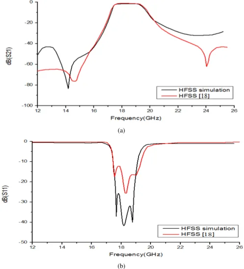
Fig. 22 illustrated the reflection coefficient S11 and the transmission coefficient S21 of SIW
(a)
(b)
Fig. 22. Frequency response of SIW bandpass filter iris with high rejection. (a) Transmission coefficient S21 as a function of frequency. (b) Reflection coefficient S11 as a function of frequency.
The results simulated by HFSS are in good agreement with the results in [18]. The results simulated
by HFSS shows that the full frequency passband is from 17.3 to 19.3 GHz. the center frequency
f0= 18.3 GHz, the absolute bandwidth 2 GHz and the relative bandwidth FBW= 10.9 %. The insertion
loss around 18.3 GHz is approximately 1.35 dB, the return loss in the passband is better than 15 dB,
with high rejection of -57.88 dB at the frequency 24.07 GHz.
This filter have a small size can be directly integrated with other circuits. This makes them
favorable for the applications of multimedia services.
V. CONCLUSION
In this work, a bandpass SIW filter with high rejection was presented for K-band applications.
Which are designed by three steps, the first is the design of the SIW bandpass filter in the K-band
based on the iris topology, the second is the design of cavity resonator SIW bandstop and finally
combine the two structures for to have a SIW bandpass filter in the K-band with high rejection.
The simulated results of this filter have shown that the passband is from 17.3 to 19.3 GHz. the
center frequency f0= 18.3 GHz, the absolute bandwidth 2 GHz and the relative bandwidth
passband is better than 15 dB, with high rejection of -57.88 dB at the frequency 24.07 GHz.
These filters are easy for integration with other planar circuit compared by using conventional
waveguide. The design method is discussed; the results from our analysis are in good agreement with
previous research done on this topic. These bandpass SIW filter with high rejection is suitable for
practical applications.
REFERENCES
[1] Garima Pathak, “Substrate integrated waveguide based RF εEεS cavity filter,” International Journal of Recent Technology and Engineering, vol. 2, pp. 46-49, 2013.
[2] Bouchra Rahali and εohammed Feham, “ Design of K-Band substrate integrated waveguide coupler, circulator and power divider,” International Journal of Information and Electronics Engineering, vol. 4, no. 1, pp. 47-53, 2014. [3] D.V.B.Murthy, Alonso Corona Chávez and José L. Olvera-Cervantes, “Design and development of miniaturized filters
using substrate integrated semicircular cavities,” International Journal of Microwave and Optical Technology, vol. 5, no. 5, pp. 287-291, 2010.
[4] Yasser Arfat, Sharad P. Singh, Sandeep Arya, Saleem Khan, “εodelling, design and parametric considerations for different dielectric materials on substrate integrated waveguide,” Wseas Transactions on Communications, vol. 13, pp. 94-98, 2014.
[5] B. H. Ahmad, Siti Sabariah Sabri and A. R. Othman, “Design of a compact X-Band substrate integrated waveguide directional coupler,” International Journal of Engineering & Technology, vol. 5, no 2, pp. 1905-1911, 2013.
[6] Yongmao Huang, Zhenhai Shao and δianfu δiu, “A substrate integrated waveguide bandpass filter using novel defected ground structure shape,” Progress In Electromagnetics Research, vol. 135, pp. 201-213, 2013.
[7] Damou Mehdi, Nouri Keltouma, Taybe Habib Chawki Bouazza and εeghnia.Feham, “Design of substrat integerated waveguide bandpass filter of SCRRs in the microstrip line,” International Journal of Engineering Research and General Science, vol. 2, pp. 302-314, 2014.
[8] M. N. Husain, G. S. Tan, K. S. Tan, “Enhanced performance of substrate integrated waveguide bandstop filter using circular and radial cavity resonator,” International Journal of Engineering and Technology, vol. 6, no. 2, pp. 1268-1277, 2014.
[9] K. Cheraghi, R. Sarraf Shirazi and Gh. εoradi, “Frequency sensitivity of a substrate integrated waveguide devices by finite element method,” International Journal of Advanced Research in Electrical, Electronics and Instrumentation Engineering, vol. 2, pp. 4580- 4584, 2013.
[10]Pozar, David ε., “εicrowave engineering, fourth edition,” John Wiley and Sons, 2012.
[11]Hemendra Kumar, Ruchira Jadhav and Sulabha Ranade, “A review on substrate integrated waveguide and its microstrip interconnect,” Journal of Electronics and Communication Engineering, vol. 3, pp. 36-40, 2012.
[12]K. Nouri, ε. Feham, εehdi Damou and Tayeb Habib Chawki Bouazza, “Design of substrate integrated waveguide micro-wave planar directional coupler,” International Journal of Scientific & Engineering Research, vol. 5, pp. 1239 -1242, 2014.
[13]Jia-Sheng Hong and ε. J. δancaster, “εicrostrip filters for RF/εicrowave applications,” John Wiley and Sons, 2001. [14]Nouri Keltouma, Feham εohammed and Adnan Saghir, “Design and characterization of tapered transition and
inductive window filter based on substrate integrated waveguide technology (SIW),” International Journal of Computer Science Issues, vol. 8, no. 3, 2011.
[15]Woon-Gi Yeo, Tae-Yoon Seo, Jae W. δee, and Choon Sik Cho, “H-Plane sectoral filtering horn antenna in PCB substrates using via fences at millimetre-wave,” Proceedings of the 37th European εicrowave Conference, pp. 818 - 821, 2007.
[16]N. εarcuvitz, “Waveguide handbook,” ε.I.T. Rad. δab. Ser, vol. 10. New York: εcGraw-Hill, 1951.
[17]D. Zelenchuk, V. Fusco, “δow insertion loss substrate integrated waveguide quasi-elliptic filters for V-band wireless personal area network applications,” IET εicrowaves, Antennas and Propagation, vol. 5, no. 8, pp. 921-927, 2010. [18]B. Zheng, Z. Zhao, and Y. δv, “A K-Band SIW filter with bypass coupling substrate integrated circular cavity (SICC)