Abstract—In this article, a high-order frequency selective band-stop EMC (electromagnetic compatibility) shield is designed using multilayer square loop while each loop resonates at the specific desired frequency.
The glass material is picked out as the preferred substrate for the designing process. In contrast to the computationally intensive numerical approaches (software), the equivalent circuit model offers a simple alternative method in FSS (frequency selective surface) analyses which is useful for quickly predicting the performance of FSS. The proposed FSS can be synthesized based on microwave filter theory and the synthesized FSS can control transmission-zero frequencies. A three zero-transmission transparent window is designed using the proposed method, in which 30dB insertion loss is achieved for 6 to 10 GHz bandwidth and optical opacity of the structure is 85%.
The response of the analytical model is compared with the results of full-wave simulation. As a result, it predicts quite well the resonant frequencies of the designed FSS.
Index Terms— Frequency Selective Surfaces, Band Stop Filter Design,
Shielding Application, Equivalent Circuit Model.
I. INTRODUCTION
Solving the periodic electromagnetic problems has been long faced with many challenges due to their complex equations.
There are a few problems that lead to the closed form relation solutions employing analytical methods. The advent of the numeric and software-based methods has opened a new horizon for communication engineering researchers. Owing to the modeling capability, any numeric software can break down a substantial act of problems. But, the software user must have a proper physical vision about the problem in order to reach the desired results. The user moves to the desired answer points using the software optimizations toolbox or trial-and-error. In a complex nature problem, the designer could not control the whole processing of the response and the design process will be very time consuming. Thus, the proper use of approximation theory is worthwhile in analytical relationships and
Design of Frequency Selective Band Stop
Shield Using Analytical Method
Mahmoud Fallah1, Alireza Ghayekhloo2 , AliAbdolali3
1-3
modeling periodic complex electromagnetic field problems. Although this approach may not lead to a final answer, it creates the initial values of the parameters in the designing process, which reduces the optimization time of the problems.
Analyzing wave interaction with periodic structure like frequency selective surface (FSS) is a complex procedure. There are approximate analytical relations for the basic unit cell shapes, some of which were studied in [1] for square and hexagon patch-strip unit cells. The conditions of applying analytical relations and the matching of this solution with the full-wave response were investigated in this reference, too. By improving the analytical relations in this article, electromagnetic filters for the application of glass in the windows of buildings were designed. The designed FSS structure was fabricated with the thin film acetate applying high electrical conductivity in the ink; then, acetate was placed on the glass substrates. Therefore, the introduced theoretical designs had the possibility of simple manufacturing. The designed filters passed the light (as the visible range of the electromagnetic spectrum) and block part of the microwave band. Thus, the indoor communication link was prevented from the outside of the building access. Also, the access to various parts of a building in the communication range from other parts could be restricted as shown in [2]. Single band [3], dual [4], and tri-band [2] structures have been developed for exploiting in the wall of the constructions. These designs filter certain frequencies. In other researches, the location of wave transmitters in certain rooms or areas of the building is assumed to be fixed and the aim is only to transmit the desired bandwidth of the designer [5-7]. This approach is entirely dependent on the geometry of the buildings, places of the transmitters, and different sensitivities of FSS to the frequency and incidence angle of the radiated wave. This approach is also investigated with active FSSs in order to electronic control and cover of the different wave band regions in the building [8]. Based on the need, the access of different rooms or halls of a building to the variety of bandwidths can be restricted from a control center. In other works, the flexible FSS design has been carried out on the glass or transparent layers in front of the light. So, it is used as a window, separating in the buildings, and glass facade of the commercial/office towers [7] [9-11].
However, in all of these papers, the design is based on the trial-and-error (or software optimization). FSS design is much easier for coding inside the room walls than glass. In the design on glass, there exist some limitations in terms of the substrate thickness (glass), electrical conductivity coefficient of glass, number of layers, and area of the metal covering the glass. However, in the case of designing FSS for inside of the room walls, none of these limitations exist and more has been done for such kind of design.
Most of the structures are designed as a single screen and considered only on one side of the regular dielectric substrate. Bandwidth is limited in these structures. In this paper, two- and three-pole filters are designed using the analytical equations with the applicable thickness of glass.
expressed. Then, the frequency response obtained from the analytical relations and full-wave methods is compared. Approximations which could be used to simplify the analytical relations are introduced according to the comparison response of full-wave method and circuit model. The purpose of applying these approximations is to establish a suitable design process for this type of FSS unit cell. Educational aspects in regularizing the design process are more important than the achieved results in this report which include two practical applications.
II. Applying analytical relations and comparison with the full-wave response
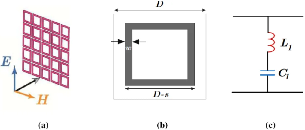
A plane wave with the polarization shown in Fig. 1-a propagates perpendicularly through FSS with the square metal ring cells. The frequency response of this structure is obtained exploiting the analytical relations. We consider FSS as a periodic metal surface without substrate in free space for a start. D, s, and w are respectively the periodicity of the rings, width of the gaps among two adjacent rings, and width of the strips. The geometrical characteristics of the unit cell are presented in Fig. 1-b. When the transverse magnetic field (in Fig. 2) faces the vertical strips, it induces current in the loop. This current leads to a secondary magnetic field around the strips, within which magnetic energy is stored. Thus, the vertical strips have an inductive effect. Further, a vertical electric field is created between the gaps of two adjacent rings. This field induces positive and negative electric charges (with alternate times change), which lead to a secondary electric field between the gaps. Thus, the horizontal gaps (in Fig. 2)have a capacitive effect. The overall effect of the arrayed structure versus the wave would be represented as an inductive component in series with a capacitive component (Fig. 1-c). A FSS should have stable performance with respect to different wave polarizations and incidence angles, since for practical applications, it would be illuminated by waves in different situations. With 90 degree rotation of the polarization, the same action happens to the horizontal strips and vertical gaps. So, the stability of the FSS can be guaranteed for different polarizations.
Fig. 1. a) Transverse electromagnetic wave (TEM) irradiates the extremely large metal array of square loops. b) Unit cell of array c) An array of square ring faces the electromagnetic wave and acts as an inductive component in series with a
capacitive component at low frequencies.
Fig. 2. Vertical strips and horizontal gaps of the arrayed square loops face the wave and act as the inductor and capacitor, respectively.
If we only look at the structure with the circuit perspective, we have to consider two parallel inductors which are equivalent to two parallel adjacent strips in a cell. The point is that the magnetic field which involves the two adjacent strips of these two loops orbits both the two strips together (Fig. 3). In other words, the magnetic field energy stored around the two parallel strips is not twice the magnetic energy of one strip with w width, but is equal to the energy of a strip with 2w width. It should be noted that it is not probably possible to fully analyze the electromagnetic structures with circuit relations.
Fig. 3. The magnetic field surrounding the two adjacent strips. Capacitive
Effect Inductive
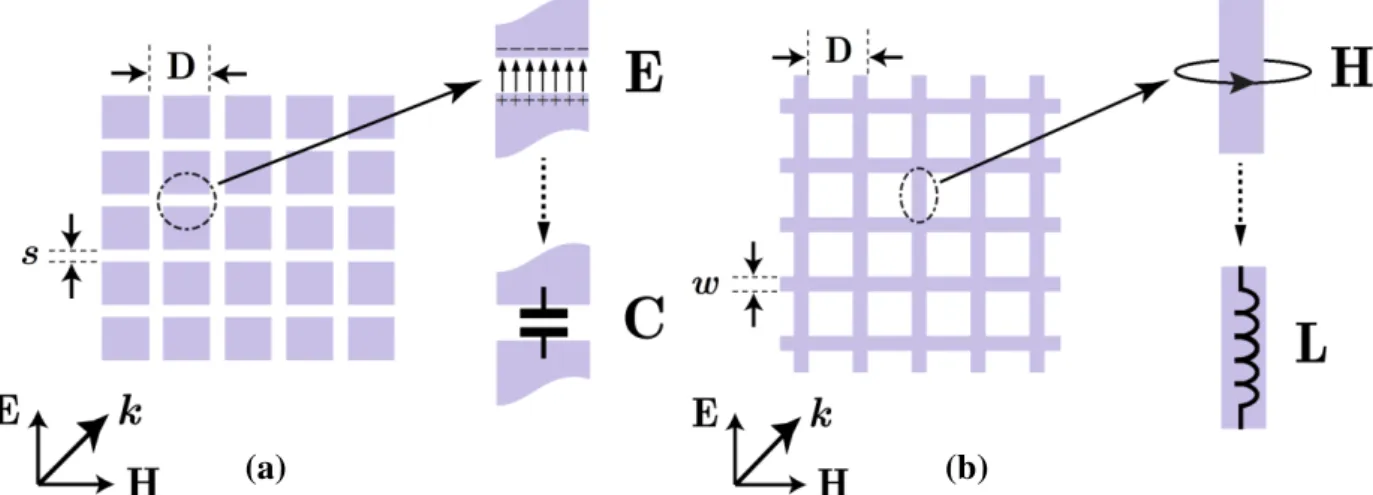
Fig. 4. (a) The geometric configuration of square patch array. This array acts as a capacitor exposed by a TEM incident wave with the shown polarization. (b) The geometric configuration of square strip array. This array acts as an inductor exposed by
a TEM incident wave with the shown polarization [12].
Values of the capacitor and inductor (in one unit cell) for an array of (horizontal) capacitive gaps and (vertical) inductive strips versus a plane wave with the shown polarization in Fig. 4 are obtained respectively from equations (1) and (2) [1,12].
(1)
) , , , ( 2 cos4
D H D s
C eff
(2)
) , , , ( 2cos
D H D w
L eff
It is assumed thatis the angle of the incident wave with the perpendicular direction to the surface,
eff
is the effective dielectric constant around the capacitive array, effis effective magnetic
permeability coefficient around the inductive array, D is the periodicity of the array, s is the width of the capacitive array gap and is wavelength. The H parameter is:
(3)
) , , , ( 2 sin ln 1 s D G D s H And the G coefficient is obtained from the following relation:
(4)
A A A A B B A A A A B B G 6 3 2 2 2 1 2 4 5 . 0 (5)
1 cos sin 2 1 1 2 D D A(6)
D s 2 sin (7)
2
2 1 1(9)
8 4 1 4 2 3 BAs it is shown in Fig. 1 to 2, the two parallel strips of the two adjacent square loops are considered as one strip with 2w thickness and space gap with the D-s overlap length. Thus, the values of the capacitance and inductance of the square ring array unit cell are respectively obtained in equations (10) and (11).
(10)
) , , , ( 2 cos ) ( 41
D H D s
D s D C eff
(11)
) , , 2 , ( 2 cos ) (1
D H D w
D s D
L eff
In Fig. 5, the transmission coefficient of an array of the square loop is analyzed in full-wave solution using CST Microwave Studio software.
The structure that we want to simulate is an unlimited periodic surface, whose constituting cell is a square conductor ring on the electric substrate. For simulating such a structure, the boundary condition "Unit cell" as a periodic boundary condition in the simulator software should be used.
A computer is only capable of calculating problems that have finite expansion; hence, we need to specify the boundary conditions. We should enter the boundaries property sheet, the modeled structure is displayed with a surrounding bounding box. So, we connect two opposite boundaries with a definable phase shift such that the calculation domain is simulated to be periodically expanded in the corresponding direction. Thus, changing one boundary to periodic state always changes the opposite boundary to the periodic state as well.
In practice, this structure can be realized by printing conductive silver ink on glass. Electrical
conductivity of this substance is2.6106 s/m. After the printing process, the printed meshed on the substrate is cured at 120ºC in an oven with atmospheric air. The thickness of the printed conductor is found to be 10 μm with the help of post curing profile measurement[13]. In CST software, the electrical conductivity of the metals used in simulations can be valued as desired. Therefore, considering that square rings are made of silver ink, electrical conductivity of this substance should be used in the simulations.
This result is compared with Equations (10) and (11) in the chart. This scenario is simulated
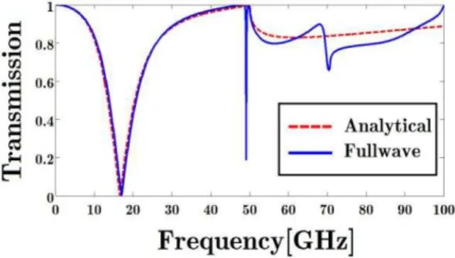
excitation source. This model is very complicated. Because H is dependent on the frequency due to the G term, the values of capacitance and inductance are dispersive in Equations (10) and (11). A complex equation has to be solved while extracting geometry of the structure for a particular resonant frequency. Now, we want to achieve the effect of the G phrase in the modeling. To find out more, we simulate it again. But in this case, the G phrase is removed from the analytical relations and results can be observed in Fig. 6. According to the results, the frequency response could be obtained by
applying the equations without the dispersive part for the area ofD. In Fig. 6, the resonant frequency of the structure employing the analytical equations is
obtained fr 1/(2 LC)17.16GHz. This result has a little difference from 17.00GHzwhich is obtained from the full-wave simulation (Fig. 6). L and C are computed without G phrase here.
Fig. 5. Comparing full-wave simulation and analytical results for the transmission coefficient of the arrayed square loop considering the dispersive part (G phrase).
Fig. 6. Comparing full-wave simulation and the analytical results for the transmission coefficient of the arrayed square loop without considering the dispersive part (G phrase).
III. APPLICATION OF MICROWAVE SHIELDING FOR GLASS
The frequency selective surfaces which transmit the visible light have many applications such as the transparent antennas and the design of electromagnetic shield windows.
block a specific microwave bandwidth and there is no need to pass other frequency components out of the band perfectly, only the transmission of the visible spectrum is important.
To begin with, we must consider two panels of the first-order band-stop FSSs on two sides of the
glass substrate with the relative permittivity coefficient of r 5.7. The two zeros of transmission
using analytical Equations (10) and (11) are f14.4GHz andf27GHz . Also, due to the
permittivity coefficient of glass and the thickness of/4, the corresponding frequency and thickness
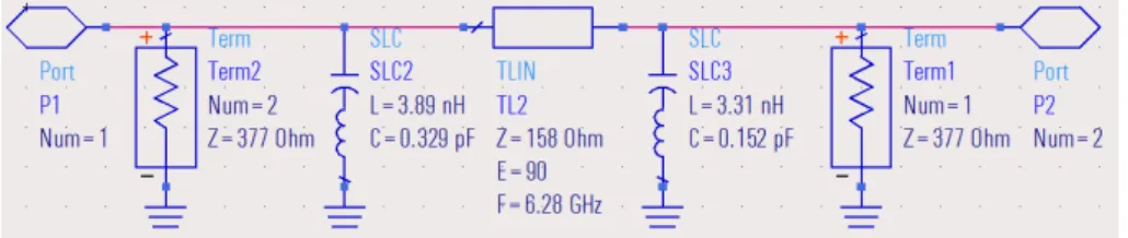
are considered about 6 GHz and 5mm, respectively. Then, f c/(4d r)6.3GHz . The equivalent circuit of the structure is shown in Fig. 7 from ADS software. The geometry values of the layers are provided in Table I from the analytical relations. In this table, h is the thickness of glass as the substrate. It should be noted that the resonant frequencies of the two surfaces are calculated separately. This means that the two surfaces are assumed to have no effect on each other's resonant frequency. If the thickness of the glass is not too small or the dielectric constant is not too high, this assumption is verified. The design process could not be ended only with the calculated resonant frequencies, but ADS software can be used to precisely adjust the circuit frequency response again.
The next step of the design procedure involves determining the initial geometric parameters of the unit-cell structure using the obtained inductor and capacitor values from the circuit model. It should be noted that the method presented in this paper consists of a part of the design processwith a trial-and-error method. The main difference of this method used here to implement in circuit software (such as ADS) is that it is very fast. However, other conventional approaches used by researchers are the trial-and-error approach in Full-wave software that takes much longer time.
Another point for increasing the accuracy is that the dispersive part (G) would be added to the analytical relations. And instead of using circuit software (ADS) to obtain the frequency response (without dispersive part), a Matlab code including dispersive part can be used, because defining dispersive inductor and capacitor in ADS is difficult.
Fig. 7. The second-order band stop filter circuit in ADS software.
Table I
The geometric parameters of the second-order band stop FSS
t
r
h w
2
s
1
s D
mm
01 . 0 7 . 5
mm
5
mm
2 . 0
mm
5 . 1
mm
5 . 0
mm
5
total area of the unit cell. There is 85% transparency in the visible range. Two curves are compared in Fig. 8 for full-wave simulation and the circuit model response. As seen in the chart, there is 25dB loss in the range of 4.7 to 7.5 GHz.
Fig. 8. Comparing full-wave and circuit model responses of the second-order band stop filter.
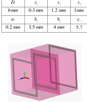
It is clear that we must make the resonant frequencies of the two-layer FSS close together if we want to have more loss in the stop band. In this case, the stop bandwidth is reduced. But, by increasing the number of FSS surfaces, an additional loss is obtained and simultaneously the bandwidth remainsconstant. In the next example (as example 2), the three-layer FSS is investigated. A scheme of the FSS is shown in Fig. 12. The geometry of the structure is provided in Table II, in
which h1andh2are the applicable thicknesses of the commercial glass. The circuit model of example
2 in ADS software is shown in Fig. 9.
Table II The geometric parameters of a third-order band stop FSS (example 2)
3
s
2
s
1
s D
mm
05 . 1
mm
3 . 1
mm
8 . 0
mm
6
r
2
h
1
h w
7 . 5
mm
5 . 3
mm
3
mm
2 . 0
Fig. 10. Comparing full-wave response and the circuit model response of the band stop third-order filter (example 2).
Fig. 10 shows the comparison of the circuit model simulation and full-wave one. As can be seen in the chart, for 2 GHz bandwidth which is similar to the previous example, there is 50 dB loss for the three-layer design. It is now expected that the bandwidth is enhanced by increasing the distance between the zeros and, in return, the loss is lessened. There is 84% transparency in the visible spectrum. In the next example (example 3), the distances between each zero are increased. The circuit model and the geometric characteristics of the structure are given in Fig. 11 and Table III, respectively.
Fig. 11. Equivalent circuit of the third-order band stop filter with the increased distance between zeros in ADS software (example 3).
Table III Geometric parameters of the third-order band stop filter (example 3) with the increased distance zeros
3
s
2
s
1
s D
mm
1
mm
2 . 1
mm
3 . 0
mm
6
r
2
h
1
h w
7 . 5
mm
4
mm
5 . 3
mm
2 . 0
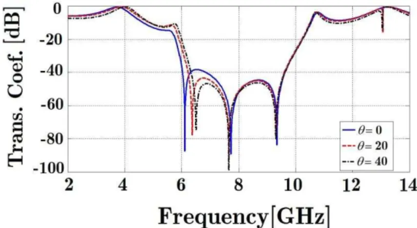
The unit cells of the structure prevent 17% of the incident light (for the normal incident case). Therefore, there is 83% transparency in the visible electromagnetic wave band. Fig. 13 is about the comparison of the results of two simulations for circuit model and full-wave method. There is 30 dB loss in the 6 to 10 GHz interval according to this figure. The transmission coefficients of FSS at various oblique angles of incidence are also calculated using full-wave EM simulations in CST software and the results are presented in Fig. 14. It is observed that the structure demonstrates a stable frequency response as the angle of incidence is increased.
Fig. 13. Comparing the full-wave response and circuit model for a band stop third-order filter with the increased distance of the zeros.
Fig. 14. Comparing full-wave responses of the band stop third-order filter for different incidence angles.
IV. CONCLUSIONS
the transparency of 83%, 30 dB loss for 6 to 10 GHz frequencies, and the stability of the electromagnetic response to the varied wave angle.
REFERENCES
[1] M. Fallah, M. H. Vadjed-Samiei, “Design of Bandpass FSS Based on Analytical Method Using Hexagon Patch-strip cell”, UEMG, Electromagnetics, vol. 35, no. 1, pp. 25–39, Dec. 2015.
[2] D. Kim, J. Yeo, J. Choi, “Compact Spatial Triple-Band-Stop Filter for Cellular/PCS/IMT-2000 Systems”, ETRI Journal, vol. 30, no. 5, Oct. 2008.
[3] R. Natarajan, M. Kanagasabai, S. Baisakhiya, R. Sivasamy, S. Palaniswamy, J. K. Pakkathillam, “A Compact Frequency Selective Surface With Stable Response for WLAN Applications”, IEEEAntennas and Wireless Propagation Letters, vol. 12, pp. 718-720, May 2013.
[4] A. Ray, M. Kahar, S. Biswas, D. Sarkar, P. P. Sarkar, “ Dual Tuned Complementary Structure Frequency Selective Surface for WLAN Applications”, Journal of Microwaves, Optoelectronics and Electromagnetic Applications, vol. 11, no. 1, Jun. 2012.
[5] M. Raspopoulos, S. Stavrou, “Frequency Selective Buildings through Frequency Selective Surfaces”, IEEE Transactions on Antennas and Propagation, vol. 59, no. 8, Aug. 2011.
[6] P. S. Taylor, A. C. M. Austin, E. A. Parker, M. J. Neve, J. C. Batchelor, J. T. -P. Yiin, M. Leung, G. B. Rowe, A. G. Williamson and K. W. Sowerby, “Angular independent frequency selective surfaces for interference control in indoor wireless environments”, Electronics Letters 19th vol. 48, no. 2, Jan. 2012.
[7] J. Roberts, J. M. Rigelsford and K. L. Ford, “Diffraction from Frequency Selective Surfaces for Secure Building Applications”, 6th European Conference on Antennas and Propagation (EUCAP), IEEE, Prague,pp. 2388-2391,Mar. 2012.
[8] L. Subrt, P. Pechac, “Controlling Propagation Environments Using Intelligent Walls”, 6th European Conference on Antennas and Propagation (EUCAP), IEEE, Prague,pp. 1-5,Mar. 2012.
[9] S. I. Sohail, K. P. Esselle, G. Kiani,“Design of a Bandpass FSS on Dual Layer Energy Saving Glass for Improved RF Communication in Modern Buildings”, Antennas and Propagation Society International Symposium (APSURSI), IEEE, Chicago, IL, pp. 1-2, Jul. 2012.
[10]L. B. Wang, K. Y. See, B. Salam, A. C. W. Lu, l. W. Zhang, S.Tengiz, “Tri-Band Frequency Selective Band-Stop Shield Using Screen Printing Technique”,Asia-Pacific Symposium on Electromagnetic Compatibility (APEMC), IEEE,
Singapore, pp. 661-664, May 2012.
[11]J. V. Rodriguez,“Radiowave Propagation through Window Panes and Reinforced Concrete Structures-An application of Frequency Selective Surface techniques”, Thesis, Department of Electroscience Lund University, 2001.
[12]M. Fallah, M. H. Vadjed samiei,"Design of Square Patch-Strip Bandpass FSS Using Equivalent Circuit Model", Journal of Modeling in Engineering, vol. 13, no. 41, sep. 2015.