Brazilian Journal of Physics, vol. 34, no. 2B, June, 2004 605
Monte Carlo Studies of Miniband Conduction
in Extreme Type-II Superlattices
A. B. Henriques
∗, R. Deacon
†, and R. J. Nicholas
†∗
Instituto de F´ısica, Universidade de S˜ao Paulo, Caixa Postal 66318, 05315-970 S˜ao Paulo, Brazil
†
Clarendon Laboratory, Oxford University, Oxford OX1 3PU, U.K.
Received on 31 March, 2003
Miniband charge transport was investigated by Monte Carlo simulations of electronic motion in short period superlattices of type-II energy band alignment (InAs/GaSb composition). The strong decrease of the miniband energy width when the electronic in-plane energy increases, characteristic of type-II superlattices, leads to a conductivity that is very sensitive to a magnetic field applied parallel to the axis of the superlattice. For structures with a miniband energy width greater than the optic phonon energy, the differential conductance can be changed from positive to negative by the magnetic field, due to the suppression of optic phonon emission.
1
Introduction
Miniband conduction in a superlattice is characterized by a negative differential resistance when the intensity of the electric field exceeds a critical value,Fc, which is required for electrons to reach high enough crystal momentum val-ues (about one third of the mini-Brillouin width), to mani-fest Bragg reflections by the superlattice [1]. The Esaki-Tsu model [2] is the simplest one to describe miniband trans-port. It assumes catastrophic scattering and leads to an an-alytical electronic drift velocity. A more complete descrip-tion, however, requires the inclusion of multiple scattering processes, with a complicated dependence of the scattering amplitude on sample parameters and external fields. In such a case, Monte Carlo simulations have been used to model the conductivity for various type-I band alignment systems [3, 4], which produces a semiclassical description in which Wannier-Stark quantization [5] is not included.
An InAs/GaSb heterojunction forms an extreme type-II band alignment, where the conduction band of InAs lies be-low the top of the valence band of GaSb. In short period InAs/GaSb superlattices, quantum confinement leads to a positive difference between the energy of conduction band and valence band states, and a semiconducting energy gap is recovered. However, in opposition to the behavior seen in type-I systems, the carrier tunneling probability between ad-jacent wells, and hence the miniband width, decreases very rapidly when the in-plane energy of the carriers increases, in sharp contrast to type-I superlattices.
In this work, we studied theoretically the miniband transport in InAs/GaSb superlattices in a quantizing mag-netic field applied along the axis of the superlattice, us-ing Monte Carlo simulations. The magnetic field causes the electronic miniband to develop into a series of Landau level minibands (LLMB). The characteristic parameters of the LLMB’s were obtained from 8-bandk·pcalculations, and they were used as input in the Monte Carlo
simula-tions. The Monte Carlo simulations showed that at low mag-netic fields, electrons gain kimag-netic energy from the external electrical field, climb the ladder of Landau levels through quasi-elastic scattering, and relax their energy through opti-cal phonon emission; in this range of magnetic fields, elec-trons may have on average a high crystal momentum, and conductivity can be high. As the magnetic field rises, the energy separation between adjacent LLMB’s increases, and ultimately a complete transition into a quantum box super-lattice transport regime is reached. The transition into the quantum box superlattice regime occurs when the funda-mental LLMB width becomes less than the cyclotron en-ergy. For high enough magnetic fields, the miniband energy width will also become less than the optical phonon energy; in this range of magnetic fields, optical phonon scattering is completely suppressed, and electron scattering becomes limited to quasi-elastic transitions between states of oppo-sitekz, leading to a low average electronic crystal momen-tum, and hence a low vertical conductivity. These effects are specific to the extreme type-II structures, in which the miniband width decreases with applied magnetic field.
2
Model
When a magnetic field is applied parallel to the axis of the superlattice, the continuous in-plane kinetic energy spec-trum of electrons, ~22k2m∗, is broken into a ladder of discrete Landau levels of energy~ωc(N+12), whereωc=eB/m∗is the in-plane cyclotron frequency for electrons. In the tight-binding approximation, the total energy spectrum of elec-trons will be given by a set of LLMB’s
E(N, kz) =~ωc
µ N+1
2 ¶
−∆
2 coskzd, (1)
606 A. B. Henriques, R. Deacon and, R. J. Nicholas
taken to be independent ofNandB, however, for a type-II superlattice,∆will be dependent on the in-plane energy. For an InAs/GaSb superlattice, we performed 8-bandk·p cal-culations, and found that the energy width of the electronic miniband,∆(N, B), on magnetic field intensity,B, can be fitted for all Landau levels, N, with a single parameter α, such that
∆(N, B) = ∆0e−
α(N+1 2)~ωc
(2) where∆0andαare parameters, obtained by fitting the
the-oretical result of thek·pcalculations with Eq. (2). Table 1 summarizes the miniband parameters obtained from the 8-bandk·pcalculations for three InAs superlat-tices: all three structures had the same thickness in the InAs layers (50 ˚A), but differed in the width of the GaSb layers (60 ˚A for structure #1, 70 ˚A for structure #2, and 80 ˚A for structure #3).
Table I. Structure parameters extracted fromk·p calcula-tions and used as input in the Monte Carlo simulacalcula-tions.
Structure period d ∆0 α
( ˚A) (meV) (eV−1)
#1 110 34.5 18.1
#2 120 24.2 21.8
#3 130 17.5 25.6
Monte Carlo calculations were done for all three struc-tures. The electric field was applied parallel to the superlat-tice axis. The natural basis states for electrons are the LLMB states|N, X, kz>: the integer for the Landau level (N), the guiding center coordinate (X), and the wavevector along the superlattice direction (kz). The effect of the electric field is taken into account using the acceleration theorem. We fol-lowed the usual Monte Carlo scheme, described in Ref.[3], which consists of modeling the motion of an electron as a se-quence of free flights interrupted by collisions. The duration of each flight, the scattering mechanism operating at the end of the flight, and the quantum state of the electron after the instantaneous scattering process, were chosen stochastically using a random number generator. At the end of the flight electrons were scattered by acoustic or optic phonons, in-cluding Umklapp processes. The average crystal momentum was computed after 500 thousand flights. All calculations were done assuming a level broadening ofγ = 0.5 meV. Figure 1 shows the average electron drift velocity as a func-tion of applied electric field, obtained from the Monte Carlo calculations for the structures described in Table 1, when
B = 0. The conductance increases when the width of the miniband increases; this is because for very short period structures, the miniband width is larger than the LO opti-cal phonon energy (~ωLO=30 meV). As a result, electrons have a very efficient route to relax their energy, i.e. by optic phonon emission, and the electrons may acquire a large av-erage crystal momentum. In contrast, if the miniband width is less than the optical phonon energy, electrons can relax energy only through quasi-elastic acoustic phonon emission. This process is much less efficient, and for the same electric field the electron’s average momentum is much smaller, due
to an increased probability of Bloch transport. Further, for a structure with a miniband width greater than~ωLO, (struc-ture #1) electrons have a small probability of acquiring crys-tal momentum beyond∼π/3d, and the negative differential conductivity regime is almost absent.
Figure 1. Electronic drift velocity as a function ofF/Fcfor
struc-tures described in Table 1.
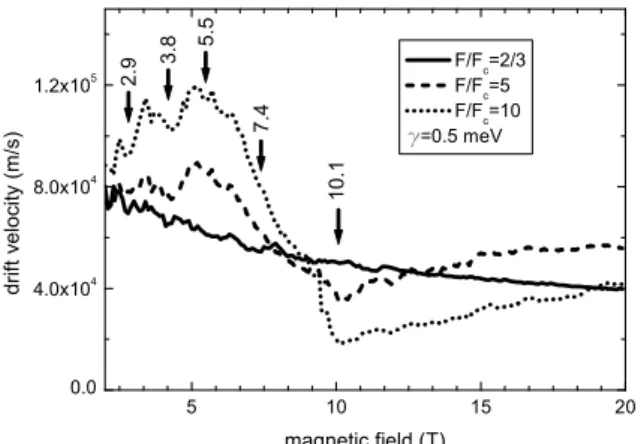
Figure 2. Electronic drift velocity as a function ofBfor structure #1 (Table 1).
Next we examine the effect of a magnetic field applied perpendicular to the layers. Figure 2 shows the calculated drift velocity,vd, for structure #1 described in Table 1, for a range of electric fields, F/Fc = 2/3, F/Fc = 5, and
Brazilian Journal of Physics, vol. 34, no. 2B, June, 2004 607
positive to one of negative differential resistance. This fea-ture is unique to type-II superlattice systems, whereby the miniband energy width depends on the in-plane kinetic en-ergy. The Monte Carlo study also shows conductivity steps at the magnetic field values where an excited Landau level is shifted out of energy resonance with the fundamental one (10.1T, 5.5T, 3.8T 2.9T,...) . At these fields, elastic inter Landau level scattering is reduced and the probability of electrons climbing the ladder of Landau levels to states with enough energy to emit an optical phonon decreases, leading to a decrease in conductivity (Fig.1). These steps, however, are not equally spaced in reciprocal field, as expected for type-I systems, due to the strong dependence of the mini-band energy width on the magnetic field.
3
Conclusion
Thek·pcalculation showed that in extreme type-II super-lattices of InAs/GaSb composition the width of the LLMB’s decrease with applied magnetic field, and the dependence of the width on magnetic field can be approximated by an ex-ponential function quite well. The Monte Carlo calculations showed that a magnetic field applied parallel to the super-lattice axis could strongly suppress conductivity, due to the
increasing isolation of the LLMB’s from one another. For structures with a zero-field miniband energy width greater than the optic phonon energy, the differential conductance can be changed from positive to negative by an applied mag-netic field, due to the suppression of optic phonon emission.
Acknowledgments
A.B.Henriques acknowledges support from FAPESP (Pro-jeto No. 99/10359-7) and CNPq (Pro(Pro-jeto No. 306335/88-3).
References
[1] Semiconductor Superlattices, edited by H.T.Grahn, World Scientific, Singapore (1995).
[2] L.Esaki and R. Tsu, IBM Journal of Research and Develop-ment 14, 61 (1970).
[3] A. Sibille, J.F.Palmier, M.Hadjazi, H.Wang, G.Etemadi, E.Dutisseuil, and F.Mollot, Superlatt. Micr. 13, 247 (1993).
[4] N. Mori, C.Hamaguchi, L.Eaves, and P.C.Main, VLSI Des.
13, 45 (2001).