UNIVERSIDADE FEDERAL DO RIO GRANDE DO NORTE
TELECOM PARISTECH
METAMATERIAL INSPIRED IMPROVED
ANTENNAS AND CIRCUITS
DAVI BIBIANO BRITO
UNIVERSIDADE FEDERAL DO RIO GRANDE DO NORTE
TELECOM PARISTECH
Metamaterial Inspired Improved Antennas and
Circuits
Davi Bibiano Brito
Natal, RN - Brazil
December 2010
D.Sc. Dissertation presented to the
Metamaterial Inspired Improved Antennas and Circuits
A Thesis Presented to The Academic Faculty
by
Davi Bibiano Brito
In Partial Fulfillment Of the Requirements for the Degree Doctor of
Science in Electrical Engineering
Advisor:
Prof. Dr. Adaildo Gomes d’Assunção (UFRN)
Advisor:
Prof. Dr. Xavier Begaud (Telecom ParisTech)
Co-Advisor: Prof. Dr. Humberto César Chaves Fernandes (UFRN)
Examiner:
Prof. Dr. José Ricardo Bergmann, (PUC-Rio)
Examiner:
Prof. Dr. Tan-Phu Vuong (INPG-Grenoble)
Examiner:
Prof. Dr. Gervásio Protásio dos Santos Cavalcante (UFPA)
Examiner:
Prof. Dr. Bernard Huyart (Telecom ParisTech)
Acknowledgements
Foremost, I would like to express my sincere gratitude to my advisors Prof. Adaildo
Gomes D’Assunção, Prof. Xavier Begaud and Prof. Humberto César Chaves Fernandes for
the continuous support of my Ph.D study and research, for their patience, motivation, and
immense knowledge. Their guidance helped me in all the time of research and writing of this
thesis. Besides my advisors, I would like to thank my fellow labmates at UFRN and Telecom
ParisTech for the stimulating discussions and for all the fun we have had in the last four years.
Last but not the least, I would like to thank my family for all their love and
encouragement. My Grandparents Rafael, Dione and Maria for their love and support. My
Uncle José for his help. For my parents Dacio e Roberta (for giving birth to me at the first
place) who raised me with a love of science and supported me in all my pursuits. And most of
all for my loving, supportive, encouraging, and patient Pollyana whose faithful support during
List of Publications
D. B. Brito, “Metamaterial Inspired Improved Antennas and Circuits”, Tese de Doutorado,
PGGEEC - UFRN, COMELEC – TELECOM PARISTECH, Natal-RN, dezembro de 2010,
102 p.
D. B. Brito, X. Begaud, A. G. D'Assuncao, and H. C. C. Fernandes, “Ultra wideband
monopole antenna with Split Ring Resonator for notching frequencies”, EuCAP 2010. 4th
European Conference on Antennas and Propagation, pp. 1 - 5, Barcelona, Espanha, Abril
2010.
D. B. Brito, X. Begaud, A. G. D'Assuncao, and H. C. C. Fernandes, “Ultra Wideband
Monopole Antenna using Split Ring Resonator”, COSTic0803 3rd Management
Committee/Working Group, Meeting and Workshop, Atenas, Grécia, Outubro 2009.
D. B. Brito, H. C. C. Fernandes, “Unilateral Fin Line Directional Coupler”. International
Table of Contents
Chapter 1 Introduction ... 15
Chapter 2 Metamaterials ... 17
2.1 Metamaterials Overview ... 17
2.2 Electromagnetic Wave Propagation in a Metamaterial Media ... 22
2.3 Artificial Materials ... 25
2.4 Bianisotropic Media ... 30
2.4.1 Double-Negative and Indefinite Media ... 31
2.4.2 Photonic and Electromagnetic Crystal ... 32
2.5 Summary ... 34
Chapter 3 Frequency Selective Surfaces ... 35
3.1 FSS Element Types ... 37
3.2 Electromagnetic Wave Propagation in a Metamaterial Media ... 38
3.2.1 Infinite FSS Arrays ... 39
3.2.2 Finite FSS Arrays ... 39
3.3 Metamaterial FSSs ... 40
3.4 Antenna Bandwidth augmentation ... 42
3.5 Summary ... 43
Chapter 4 Microstrip Antennas and Filters with CSRR Parasitic Structures ... 44
4.1 Ultra Wideband Monopole Antenna with Split Ring Resonator as Filter ... 45
4.1.1 Complementary Split Ring Resonator ... 50
4.1.2 Simulation and Experimental Results ... 51
4.2 CSRR Stop Band Filter ... 62
4.3 Summary ... 65
Chapter 5 Microstrip Antennas with HIS Ground Plane ... 67
5.1 High Impedance Surfaces ... 68
5.2 Microstrip Patch Antenna with HIS Ground Plane ... 70
5.3 Suspended U-Slot antenna on HIS Substrate ... 78
5.4 Summary ... 81
Chapter 6 Fabry-Pérot Antennas ... 83
6.1 Fabry-Pérot Interferometer ... 83
6.2 The Fabry-Pérot Antenna ... 85
6.2.1 Fabry-Pérot Patch Antenna ... 86
6.2.2 Fabry-Pérot Suspended U-Slot Antenna ... 90
6.3 Summary ... 93
Chapter 7 Conclusions ... 94
List of Acronyms and Symbols
Nabla operator
B Magnetic field c Velocity of light
CSRR Complementary Split Ring Resonator
D Electric displacement field DNG Double-Negative
DPS Double-Positive
E Electric field
EBG Electromagnetic Band-Gap ENG Epsilon-negative
ε0 Free space permittivity εeff Effective permittivity
εr Relative permittivity
FSS Frequency Selective Surfaces FP Fabry-Pérot
H Magnetizing field HIS High Impedance Surface
k Wave vector
LHM Left Handed Metamaterial
λ Wavelength
λ0 Free space wavelength
λg Guided wavelength MNG Mu-Negative
µ0 Free space permeability µeff Effective permeability
µr Relative permeability
! Index of refraction PCB Printed Circuit Board
PEC Perfectly Electrically Conducting RF Radio Frequency
S Poynting vector
SNG Single-Negative SRR Split Ring Resonator
σ Conductivity of the metal TW Thin-Wire
List of Figures
Figure. 2.1 Diagram showing the Poynting vector of an electromagnetic wave. On left
normal materials, and on the right metamaterials ... 18
Figure. 2.2 Ray diagram of interface between n>0 and n<0 media ... 19
Figure. 2.3 A diagram showing the possible domains of electromagnetic materials and wave refraction having the same sign. Waves are refracted positively in conventional materials and negatively in LHM ... 20
Figure. 2.4 Ray diagram showing the direction of wave propagation ... 21
Figure. 2.5 The geometry of a generic artificial dielectric ... 21
Figure. 2.6 The geometry of wire medium: a lattice of parallel conducting thin wires ... 26
Figure. 2.7 Metamaterials constructed with common dielectrics and metals: (a) negative permittivity and positive permeability, (b) negative permeability and positive permittivity, and (c) double negative media DNG [15] ... 26
Figure. 2.8 Equivalent circuit model for the Split Ring Resonator, double and simple rig configurations ... 28
Figure. 2.9 Theoretical results for: (a) permittivity using a SRR and (b) permeability using a thin wire ... 29
Figure. 2.10 Bianisotropic particles: (a) chiral, (b) omega, and (c) double chiral ... 30
Figure. 2.11 Realization of DNG material at microwave frequencies ... 31
Figure. 2.12 The blue-green color on several species of butterflies is caused by the nanoscale structure of the insects’ wings ... 32
Figure. 2.13 The first photonic crystal with a complete band gap [19] ... 33
Figure. 2.14 Ultra wideband Bowtie antenna with HIS substrate ... 33
Figure 3.1 Electron in the plane oscillates due to the force exerted by incident wave resulting in low transmittance ... 36
Figure 3.2 Electron is constrained to move and hence unable to absorb energy resulting in high transmittance ... 36
Figure 3.3 Metal screen irradiated by a normally incident plane wave [1] ... 37
Figure 3.4 Basic FSS geometries: The patch-array produces a capacitive response, whereas the array of slots is inductive. ... 38
Figure 3.7 Superior view of a high impedance surface, with patches connected to the
ground plane with metal cylinders [32] ... 41
Figure 3.6 A corrugated reactive surface acting as an AMC ... 41
Figure 3.8 Origin of the equivalent circuit elements left and equivalent circuit model for the high-impedance surface right ... 42
Figure 4.1 Ultra wideband and UN-II spectrum ... 44
Figure 4.2 Circular microstrip monopole antenna, the gray region denotes a conductor material ... 47
Figure. 4.3 (a) Return loss and (b) Smith Chart results for the microstrip circular monopole antenna ... 48
Figure 4.4 Circular microstrip monopole antenna with improved ground plane, where the gray region denotes a conductor material ... 49
Figure 4.5 Return loss for the improved microstrip circular monopole antenna ... 49
Figure 4.6 Geometries and equivalent circuit of a SRR and a CSRR, where the gray region denotes a conductor material ... 51
Figure 4.7 UWB antenna with CSRR top view and the CRSS structure bottom view: the gray region denotes a conductor material ... 52
Figure 4.8 Monopole antenna with different CSRR configurations ... 52
Figure 4.9 Return loss for different CSRR configurations, red microstrip line top center, green patch’s center and blue patch’s right center ... 53
Figure 4.10 Constructed antenna ... 54
Figure 4.11 LPKF ProtoMat® printed circuit board prototyping machine ... 55
Figure 4.12 Return loss for the microstrip circular monopole antenna, in red color measured and in blue simulated results ... 56
Figure 4.13 Realized gain 3D pattern at: (a) 4GHz, (b) 5.9GHZ and 6.5 GHz ... 56
Figure 4.14 Anechoic chamber utilized in the measurements ... 57
Figure 4.15 Measurement schema used to determine the radiation pattern ... 58
Figure 4.16 Farfield radiation patterns, E-plane, on left, results and H-plane, on right, results: (a) 4GHz, (b) 5.9 GHZ and 6.5GHz, blue simulated and red measured ... 59
Figure 4.17 FCC mask ... 60
Figure 4.18 FCC pulse ... 60
Figure 4.20 Group delay from two microstrip monopole antenna with CSRR filter inserted
in the conductor patch ... 61
Figure 4.21 CSRR stop band filter top. The gray region denotes a conductor material ... 63
Figure 4.22 CSRR geometries. The gray region denotes a conductor material ... 63
Figure 4.23 Simulated S11 and S21 parameters for the metamaterial based stop band with single CSRR ... 64
Figure 4.24 Three-period CSRR stop band filter, the gray region denotes a conductor material ... 65
Figure 4.25 CSRR based filter prototype ... 65
Figure 4.26 S11 (a) and S21 (b) parameters for the metamaterial-based stop band filter with three CSRRs etched do the ground plane: blue simulated and red measured ... 66
Figure 5.1 Cross-section of a high-impedance surface ... 68
Figure 5.2 A patch antenna on a metal ground plane ... 69
Figure 5.3 A patch antenna embedded in a high-impedance ground plane ... 70
Figure 5.4 HIS superior view on the left and transversal cut on the right ... 70
Figure 5.5 Reflection coefficient for the mushroom type HIS ... 72
Figure 5.6 Patch antenna inserted in the HIS medium ... 73
Figure 5.7 Surface current at 13.23 GHz in the bandgap frequency center ... 73
Figure 5.8 S11 simulation for patch antennas on two different ground planes ... 74
Figure 5.9 Constructed structure right superior front view and left superior back view .... 75
Figure 5.10 LPKF MiniContac RS ... 75
Figure 5.11 Return loss simulated and measured for the patch antenna on a high-impedance ground plane ... 76
Figure 5.12 Farfield realized gain radiation patterns for the, E-plane on the left and H-plane on the left, blue simulated and red measured results: (a) 12.75 GHz, (b) 12.95 GHz and (c) 13.15 GHz ... 77
Figure 5.13 Reflection coefficient for the mushroom type HIS ... 78
Figure 5.14 U-slot antenna and its dimensions ... 79
Figure 5.15 Suspended U-Slot antenna backed by a HIS medium ... 79
Figure 5.16 Constructed prototype right superior front view and left superior back view .. 80
Figure 5.17 Simulated and measured return loss for the suspended U-slot antenna on a HIS ground plane ... 80
Figure 5.19 Farfield realized gain radiation patterns for the, E-plane on the left and H-plane on the left, blue simulated and red measured results: (a) 3.75 GHz, (b) 4.66
GHz and (c) 5.1 GHz ... 82
Figure 6.1 Illustration of the phenomenon due to the multiple reflections and leaky waves ... 83
Figure 6.2 Graphical representation of a plane light wave with amplitude A(i) focusing on a plate with flat and parallel surfaces. The nth reflected beam is represented by ap(r) while the nth transmitted beam is represented by ap(t) ... 84
Figure 6.3 Positioning of the Fabry-Pérot when allocated in a collimated space ... 85
Figure 6.4 Square FSS used as the antenna superstrate ... 86
Figure 6.5 Fabry-Pérot patch antenna prototype ... 87
Figure 6.6 Return loss for the Fabry-Pérot patch antenna ... 87
Figure 6.7 Fabry-Pérot antenna mounted in the anechoic chamber ... 88
Figure 6.8 Realized gain for the Fabry-Pérot patch antenna E-plane on the left and H-plane on the left: (a) 12.7 GHz, (b) 12.9 GHz and (c) 13.1. Blue simulated and red measured resuts ... 89
Figure 6.9 Constructed suspended U-slot Fabry-Pérot antenna ... 90
Figure 6.10 Fabry-Pérot antenna mounted in the ground plane ... 91
Figure 6.11 Return loss for the suspended U-slot antenna ... 91
List of Tables
Abstract
Metamaterials exhibiting negative refraction have attracted a great amount of attention
in recent years mostly due to their exquisite electromagnetic properties. These materials are
artificial structures that exhibit characteristics not found in nature. It is possible to obtain a
metamaterial by combining artificial structures periodically. We investigated the unique
properties of Split Ring Resonators, High impedance Surfaces and Frequency Selective
Surfaces and composite metamaterials. We have successfully demonstrated the practical use
of these structures in antennas and circuits. We experimentally confirmed that composite
metamaterial can improve the performance of the structures considered in this thesis, at the
frequencies where electromagnetic band gap transmission takes place.
Keywords: Left-Handed Material, Metamaterial, Split Ring Resonator, Negative Permittivity,
Negative Permeability, High Impedance Surface, Frequency Selective Surface,
Chapter 1
Introduction
Recently developments in electromagnetics in the radio frequency to optical spectral
ranges and novel fabrication techniques offer a great number of exciting new applications.
These structures are called metamaterials and they have electromagnetic characteristics that
do not occur or are not readily available in natural materials.
The purpose of this thesis is to develop new structures, for communication systems
that can provide improved functionality and performance. The great potential of
metamaterials to develop such novel structures offers an alternative with potential to
overcome limitations of current solutions. In this context metamaterials is a breakthrough,
mainly to their exquisite material properties and ability to guide and control electromagnetic
waves in a way that natural occurring materials cannot.
The thesis is organized into seven chapters. Chapter 2 presents the general theory of
metamaterials that enables its characterization, including the behavior of electromagnetic
waves explained through the Maxwell`s equations. Metamaterials, which have special optical
properties such as a negative refractive index are described. Metamaterials examples like the
Split Ring Resonator (SRR) and the High Impedance Surface (HIS) that will be used in this
thesis are presented.
In Chapter 3 the Frequency Selective Surfaces (FSS) are studied with a brief stated of
art, types and forms of the most used structures and some applications are presented. The
typical behavior of the most common element types available to the FSS designers are
discussed. The Frequency Selective Surface theory is considered starting with a comparison
of available elements to the metamaterial FSS variants. Finally this section ends with a
discussion of wideband radiating arrays.
Chapter 4 describes the use of a Complementary Split Ring Resonator (CSRR) in two
metamaterials applications; in the first the CSRR is placed as a parasite element in the
stop band filter for blocking the Unlicensed National Information Infrastructure (UN-II) band
between 5 GHz to 6 GHz. The second application is a microstrip filter that is used as an
alternative for blocking the UN-II band. The band-notched characteristic is achieved by
etching a CSRR structure in the ground plane of a microstrip transmission line. It has been
demonstrated that CSRR etched in the ground plane of a planar transmission media
(microstrip) provides a negative effective permittivity to the structure.
In Chapter 5 a HIS metallic electromagnetic structure is used as ground plane in two
directive antennas, a patch antenna and a suspended U-Shaped antenna. This structure is
characterized by having high surface impedance. Unlike normal conductors, this surface does
not support propagating surface waves, and it reflects electromagnetic waves with no phase
reversal, which can be used to improve the antennas performance.
Chapter 6 describes the use of the Fabry-Pérot (FP) optical concept as an alternative to
produce highly directive antennas. This FP medium is formed employing a HIS as a
metamaterial substrate and a FSS as a partially reflecting surface (PRS) superstrate. The used
antennas are those described in Chapter 5. This configuration leads to single feed and low
profile highly directive antennas. In addition some optical concepts are presented for a better
Chapter 2
Metamaterials
There have been a large number of definitions for metamaterials [1-8], they can be
generally defined as a class of ‘‘artificial’’ media, exhibiting extraordinary electromagnetic
properties that cannot be found in natural ones [1]. The name given to this structurally altered
materials is based on the Greek µετά (meta) that means “beyond”. The subject of
metamaterials have seen many exciting applications and has drawn considerable attention
from both the physics and engineering communities worldwide. The interest for both
communities can be explained by the fact that physicists normally study the way nature works
while engineers try to apply the knowledge and metamaterials can be place in between
science and engineering.
From the point of view of fundamental science nothing is new in metamaterials theory.
Throughout this chapter, it will be shown that metamaterials can be understood by using
well-known theoretical tools, however, almost all new applications arising from metamaterial
concepts can be understood by using more conventional approaches, that is, without the need
to invoke these metamaterial concepts.
2.1 Metamaterials Overview
During the research process to write this document the first attempt to explore the
concept of “artificial” materials appears back to 1898 when J. C. Bose [9] conducted the first
microwave experiment on twisted structures, geometries that were essentially artificial chiral1
elements by today’s terminology. In 1905, Lamb [10] suggested the existence of backward
permeability. Since then, artificial complex materials have been the subject of research
worldwide.
A key feature of these artificial materials is the negative refraction, that some titles
leads to the given name "left handed materials" (LHM), materials that refract light in a way
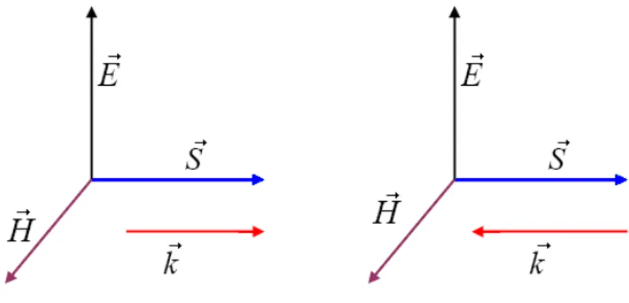
which is contrary to the normal "right handed" rules of electromagnetism, Fig. 2.1. When an
electromagnetic wave passes through this material the electric vector !, the electromagnetic
vector ! and the wave vector ! do not abide the right-handed law. The first study of general
properties of wave propagation in such a LHM medium has been attributed to Veselago [11].
In his work he showed that a plate of material with negative index of refraction would focus
light in the same way that a curved lens made with conventional materials, in the absence of
any material that had these properties. This initial work fell into obscurity.
Fig. 2.1 – Diagram showing the Poynting vectors of an electromagnetic wave. On left, normal materials, and on the right metamaterials.
Permittivity (ε) and permeability (µ) are two parameters used to characterize the
electric and magnetic properties of materials interacting with the electromagnetic fields. The
permittivity is a measure of how much a medium changes to absorb electrical energy when
subjected to an electric field. It relates ! and !, where ! is the electric displacement by the
medium and ! is the electric field strength. The common term dielectric constant is the ratio
of permittivity of the material to that of free space (ε0 = 8.85×10⁻¹²). It is also named as the
relative permittivity. Permeability is a constant of proportionality that exists between
magnetic induction and magnetic field intensity. Free space permeability µ0 is approximately
1.257×10⁻⁶ [1].
1In geometry, a figure is chiral, and said to have chirality, if it is not identical to its mirror image, or more
As mentioned before, Electric permittivity and magnetic permeability are the
parameters that determine the electric and magnetic properties of materials. Together they
determine the material's response to electromagnetic radiation. In ordinary materials both
permittivity and permeability are positive. However, for such metamaterials the effective
permittivity and effective permeability are negative values but the propagation of
electromagnetic waves is still possible since their product remains positive.
In this case, the refractive index in the Snell's law2 is negative, an incident wave
experiences a negative refraction at an interface, and we have a backward wave for which the
phase of the waves moves in the direction opposite to the direction of the energy flow [3].
Assuming an isotropic medium, the ray diagram for an interface between a medium with a
positive index of refraction and a LHM can be seen in Fig. 2.2.
Fig. 2.2 – Ray diagram of interface between n>0 and n<0 media.
The diagram shown in Fig. 2.2 can be explained by using Snell’s law. For the case
where the refractive index is positive for both media the ray could pass through the interface.
When the refractive indexes are !! >0 and !
! <0 the transmitted beam travels through the
second medium on the same side of the incident wave in the normal direction [7]. The
resulting wave moves backwards. That can be explained with the help of Fig. 2.1 were the
poynting vector !is in the direction of energy flow and continues in the same direction as in a
normal material but the wave vector k propagates in the negative direction.
η=± µμε (2.1)
2In optics and physics, Snell's law (also known as Descartes' law, the Snell–Descartes law, and the law of
Ziolkowski [5] has categorized metamaterials by their constitutive parameters as
described in Fig. 2.3. In the equation 2.1 the ± sign is assumed for general proposes. The four
possible combinations for the sign of ε and µ are (+,+), (+,-), (-,+) and (-,-). Most of the
materials in nature have positive permittivity and permeability, and hence, they are referred to
as double-positive (DPS) media. In contrast, if both of these quantities are negative, they are
called double-negative (DNG) or LHMs.
Therefore, materials with one negative parameter are named single-negative (SNG)
and are further classified into two subcategories, namely, epsilon-negative (ENG) and
mu-negative (MNG). Interestingly, natural materials such as cold plasma and silver exhibit
negative permittivities at microwave and optical frequencies, respectively, and ferromagnetic
materials exhibit a negative permeability behavior in the VHF and UHF regimes. However, to
date, no materials that exhibit simultaneous negative permittivity and permeability have been
found in nature, so, they must be designed artificially.
Fig. 2.3 – A diagram showing the possible domains of electromagnetic materials and wave refraction having the same sign. Waves are refracted positively in conventional materials and negatively in LHMs.
The arrows in Fig. 2.3 represent wave vector directions in each medium. There is wave
transmission only when both parameters waves in which the phase propagates in a direction
rays for normal materials (isotropic) and metamaterials is shown in Fig. 2.4, when a wave is
obliquely incident to the material. It may be noted in the natural materials that have refraction
in the first interface is up compared to normal while in the artificial material is down.
Fig. 2.4 – Ray diagram showing the direction of wave propagation.
Artificial dielectrics, the first known metamaterials, usually consist of artificially
created molecules: dielectric or metallic inclusions of a certain shape. These molecules can be
distributed and oriented in space, either in a regular lattice or in a random manner one
example of such organization is given in Fig. 2.5 [1].
Fig. 2.5 – The geometry of a generic artificial dielectric.
The dimensions of the molecules and the characteristic distance between neighboring
a single inclusion is usually much smaller than that of a real molecule in a network of natural
crystals. This consideration allows the description of the inclusions in terms of material
parameters and the resulting metamaterial can be characterized using Maxwell equations [1].
2.2 Electromagnetic Wave Propagation in a Metamaterial Media
Starting with the Maxwell equations reduced to the wave equation [11]:
∇!−!!
!! !!
!!! ψ= 0 (2.2)
where “η” is the refractive index, “c” is the velocity of light in vacuum, and n2/c2 = µε.
Knowing that the squared refractive index “η2” is not affected by a simultaneous change of
sign in µ and ε, it can be noted that the low-loss left-handed media must be transparent.
Considering the above equation, it can be observed that its solutions will remain unchanged
after a simultaneous change of the signs of µ and ε. The general expressions of a plane wave
are:
E =E!!!!
!!
(2.3)
H =H!!!!
!!
(2.4)
where E! and H! are vectors in arbitrary directions, k is the vector propagation constant
whose magnitude is k and whose direction is the direction of propagation of the wave and r is
the observation position vector.
k =k!x+k!y+k!z (2.5)
k = !!!+!!!+!
!! (2.6)
Instead of solving Maxwell’s equations directly to obtain wave solutions, we will
transform the system of first order partial differential equations into a single second order
partial differential equations that is easier to solve. We start with Maxwell’s equations in time
harmonic form,
∇×E= −jωB (2.8)
∇×H= jωD+J (2.9)
Knowing that,
∇∙B= ∇∙µμH= 0 (2.10)
∇∙D= ∇∙εE= !! (2.11)
Equations 2.8 and 2.9 can be rewritten as,
∇×E= −jωµμH (2.12)
∇×H= jωεE+J (2.13)
In order to handle lossy materials, we first rewrite Ampere’s Law. If we have a
medium which has free charge allowing current flow, then J= !E, and
∇×H= jωεE+!E=jω ε+ !
!! E (2.14)
∇×H= jωεE+!E=jω ε−j!
!
!
!"
E (2.15)
This shows that in the phasor domain, the conductivity can be lumped together with
the permittivity to produce a new effective complex permittivity:
!!" =ε−!! ! =
!! !
!−j
!
!!! =
A different notation can be used,
!!" =!′−!"′ (2.17)
for the real and imaginary parts of the complex permittivity. This reduces Ampere’s law for a
lossy material into the form
∇×H= jεωE (2.18)
where ε is complex. It can be shown that we have the following relations for the field vectors
and the propagation direction.
E ⊥H ⊥k (2.19)
H =!!!×E (2.20)
E =!H×! (2.21)
For the plane-wave fields of the kind E= E!exp −jk∙r+jωt and H =H!exp −jk∙
r+jωt , equations 2.12 and 2.18 can be reduced to:
k×E=ωµμH (2.22)
k×H=−ωεE (2.23)
Therefore, for positive µ and ε, E, H and k form a right-handed orthogonal system of
vectors, Fig 2.1 (a). However, if µ < 0 and ε < 0, equations 2.22 and 2.23 can be rewritten as
k×E=−ωµμ H (2.24)
In this case it can be shown that E, H and k form a left-handed triplet, as illustrated in
Figure 2.1. This result mathematically demonstrates the original reason for the denomination
of negative µ and ε media as “left-handed” media [6]. The main physical implication of the
aforementioned analysis is backward-wave propagation. The direction of the time-averaged
flux of energy is determined by the real part of the Poynting vector,
S= !
!E×H
∗ (2.26)
which is unaffected by a simultaneous change of sign of µ and ε. Thus, E, H and S still form a
right-handed triplet in a left-handed medium. Therefore, in such media, energy and
wavefronts travel in opposite directions (backward propagation). However, backward-wave
propagation in unbounded homogeneous isotropic media seems to be a unique property of
left-handed media. As it will be shown, most of the unique electromagnetic properties of these
media arise from this backward propagation property.
2.3 Artificial Materials
The concept of artificial dielectric materials was first introduced by Kock [12], and
used in the design of low-profile dielectric lens at microwave frequencies. An example of
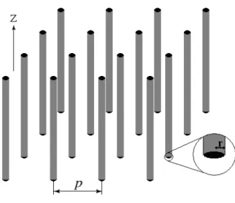
artificial dielectric is a wired medium, Fig. 2.6, which was introduced in the 1950s. The
permittivity in a medium of wires that has a frequency dependence of the plasma type
frequency dependence that is negative below the plasma frequency but small and positive
above this frequency. This structure has a negative permittivity and positive permeability.
The first real artificial metamaterial structure was designed and experimentally
demonstrated by Smith [13]. This structure was inspired by the work of Pendry [14] who
introduced the structure shown in Fig. 2.7b. This structure like the wired medium can be
designed to have a plasmatic type frequency dependence in the microwave range. This
Fig. 2.6 – The geometry of wire medium: a lattice of parallel conducting thin wires.
In the structure shown in Fig. 2.7a if the excitation electric field E is parallel to the
axis of the wires E∥ z we have from [15]:
ε
! ω = 1− !!"!
!!!!!"= 1− !!"! !!!!!+j
!!!"!
! !!!!! (2.27)
where ω!"! = 2πc!/ p!ln p/r (c: speed of light) is the electric plasma frequency, and
ζ= ε! pω!"/r !/πσ (σ: conductivity of the metal) is the damping factor due to metal losses.
From [15] we have that:
Re ε
! <0, for ω! <ω!"! −ζ! (2.28)
if ζ=0 from [15] we have,
ε
! <0 for ω<ω!". (2.29)
The permeability is != µμ!, since there is no magnetic material present (µμ! =1). The
structure shown in Fig. 2.7b if the excitation magnetic field H is perpendicular to the plane of
the rings H⊥y from [15],
µμ! ω = 1− !!!
!!!!!"! !!!!=1−
!!! !!!!!"! !!!!!"! !! !! !
+j !!!!
!!!!!"! !! !!! (2.30)
where F=π r/p !, ω!"=c !"
!!"!"!!/! is a magnetic resonance frequency, and ζ =2pR! (R!:
metal resistance per unit length) is the damping factor due to metal losses. From [15]
Equation 2.30 reveals that a frequency range can exist in which Re µμ
! < 0 in general
ζ≠0 . In the lossless case ζ≠ 0 , it appears that [15],
µμ! <0, for ω!" <! < !!"
!!! =ω!" (2.31)
where ω
An essential difference between the plasmonic expressions for ε and µμ is that the latter
is of resonant nature µμ ω=ω!" = ∞ , whereas the former is a non-resonant expression.
The resonance of the structure is due to the resonance of its SRRs, given in [15] by
ω!"! =3pc!/ πln 2d/s r! .
The pair of concentric rings shown (Fig. 2.7b) is an artificial magnetic material formed
by resonant metallic elements. This structure is called Split Ring Resonator (SRR) and due to
the small gap between the rings the structure has a larger resonant wavelength then the
diameter of the rings. This small space also produces high capacitive values, which reduce the
value of the resonance frequency. A magnetic flux penetrating the rings induces a current in
the rings that will produce its own current flow that increases or is oppose to the incident
field. It results in low radiative losses and in the high value of quality factor. At frequencies
below the resonance frequency the real part of the permittivity becomes positive and at
frequencies above the resonance becomes negative. This negative permeability along with the
negative permittivity of the wire allows the construction of a metamaterial structure shown in
Fig. 2.7c.
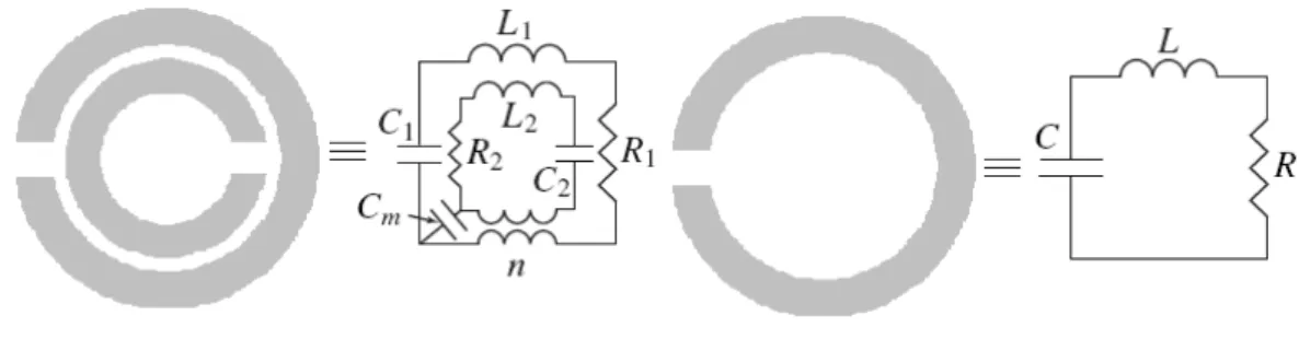
The equivalent circuit of a SRR is shown in Fig 2.8 [15]. In the double ring
configuration (left), capacitive coupling and inductive coupling between the larger and
smaller rings are modeled by a coupling capacitance (Cm) and by a transformer (transforming
ratio n), respectively. In the single ring configuration (right), the circuit model is that of the
simplest RLC resonator with resonant frequency ω! =1/ LC. The double SRR is essentially
equivalent to the single SRR if mutual coupling is weak, because the dimensions of the two
rings are very close to each other, so that L1 ≈ L2 ≈ L and C1 ≈ C2 ≈ C, resulting in a
combined resonance frequency close to that of the single SRR with same dimensions but with
a larger magnetic moment due to higher current density.
The split-ring resonators are widely used since they can be manufactured using printed
circuit technology. The artificial magnetic material with frequency-dependent positive
permeability has also been synthesized by using double circular ring resonators. An artificial
magnetic material, which is formed by split-ring resonators, exhibits negative permeability
within a frequency band (bandwidth is typically narrow) near the resonant frequency of the
single split-ring resonator; it is widely used to create LHMs. Theoretical results for the
permeability using a thin wire and permittivity using a SRR are shown in Fig. 2.9, the results
were obtained from equations 2.27 and 2.30, the substrate material is considered vacuum and
a Perfectly Electrically Conducting (PEC) as the material for the CSRR.
(a)
(b)
2.4 Bianisotropic Media
Considering the Maxwell’s theory of macroscopic electromagnetism, material media
are described phenomenologically by constitutive relations. Depending on the particular form
of the constitutive relations, a medium can be characterized as linear or nonlinear; conducting
or non-conducting; dispersive or non-dispersive; homogeneous or inhomogeneous; isotropic,
anisotropic, or bianisotropic. An isotropic medium is characterized by a scalar permittivity
that relates D to E, and by a permeability that relates H to B. In an anisotropic medium, either
or both of the permittivity and the permeability can assume the form of a three-dimensional
tensor. The constitutive relations of a bianisotropic medium relates D to both E and B, and H
to both E and B. Similarly to the anisotropic case, their relationships are provided by three-dimensional tensors [16]. When all four tensors become scalar quantities, the medium may be
called bi-isotropic. Just like an isotropic medium or an anisotropic medium, which provides a
phenomenological description of many physical media, a bianisotropic medium can also be
realized by a large class of material [16].
A generalization of this phenomenon is the bianisotropic which is associated with the
simultaneous presence of both anisotropic and magnetoelectric behavior, e.g. particles chiral
and omega shown in Fig. 210. The insulation behavior can not be described in terms of
permittivity and permeability due to the electromagnetic coupling effects between the sets of
inclusions that affect their performance, as a result the electric field not only induces electric
polarization, but also magnetic. The same is true for the magnetic field, materials that have
this characteristic are called bianisotropic [1].
Fig. 2.10 – Bianisotropic particles: (a) chiral, (b) omega, and (c) double chiral.
The bianisotropic medium is the most general type of material that can be described in
terms of normal material parameters. They have been used in many applications, such as the
These bianisotropic materials are anisotropic and can be characterized by uniaxial permittivity
and permeability tensors [18].
ε= ε! ε !! 0 0 0 ε !! 0 0 0 ε !! (2.32)
µμ=µμ!
µμ!! 0 0 0 µμ!! 0 0 0 µμ!! (2.33)
2.4.1 Double-Negative and Indefinite Media
A material will be denoted throughout as a double positive (DPS) medium if its
relative permittivity ε
!= ε/ε! and permeability µμ! = µμ/µμ! are both positive. On the other
hand, the relative permittivity and permeability are both negative in a double negative (DNG)
medium [6].
The DNG media, materials with both negative permittivity and permeability, have
become almost synonymous with metamaterials. One way to build a uniaxial DNG is to use
the structure described in Fig. 2.7c that was suggested by Pendry [13]. This structure can be
seen in Fig. 2.11 in three-dimensional form, where the arrangement of wires allows the
realization of negative permittivity and the network of SRR the negative permeability.
2.4.2 Photonic and Electromagnetic Band Gaps
The electromagnetic crystals, or photonic crystals, when operating at optical
frequencies are often termed electromagnetic band-gap (EBG) or photonic band-gap (PBG)
materials. These crystals are structures composed of electromagnetic periodic dielectric or
metallo-dielectric, operating at wavelengths that are comparable to the period, and one of its
characteristics is that they have passbands and stopbands, which affect the propagation of
electromagnetic waves [1].
Basically, these crystals contain regularly repeating internal regions of high and low
dielectric constant. Electrons or photons behaving as waves, propagate, or not, through this
structure depending on their wavelength. Wavelengths that are allowed to travel are known as
modes, and groups of allowed modes form bands. Disallowed bands of wavelengths are called
electromagnetic or photonic band gaps.
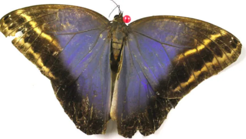
Moreover, these PBG or EBG occur in natural biological systems, for example the
color generating nanoarchitectures in the cover scales of the Morpho butterflies that use
multiple layers of cuticle and air to produce striking blue color, as shown in Fig. 2.12.
Courtesy of Prof. Dr. Dacio Rocha Brito from Uneal
Fig. 2.12 – The blue-green color on several species of butterflies is caused by the nanoscale structure of the insects’ wings.
The first studies and demonstration of a photonic crystal with a complete bandgap, see
Fig. 2.13, were carried out in the early 1990s [19]. Since then, photonic and electromagnetic
crystals have found numerous applications in FSSs and as components for waveguide and
Fig. 2.13 – The first photonic crystal with a complete band gap [19].
Electromagnetic crystals are also classified as electromagnetic bandgap structures and
high-impedance surfaces at microwave frequencies. Some practical applications of EBGs
include antenna beam narrowing and shaping using Fabry-Perot like EBG cavity [20], mobile
antenna efficiency improvement using Mushroom-like EBGs [21] amongst others. Typical
HISs are thin composite layers with reflection coefficient +1, and hence, the HIS behaves as
though it were a magnetic conductor. For this reason, HIS’s are also referred to as artificial
magnetic conductors (AMCs). An example of a HIS application is shown in Fig. 2.14 from
[22]. In this application a bowtie wideband antenna is place above a HIS substrate.
2.5 Summary
In this chapter a detailed discussion about the theoretical background of metamaterials
was presented. We provided theoretical information about the components of a left-handed
material, negative permittivity and negative permeability structures. We also showed that the
simultaneous negative values for permittivity and permeability results in negative refraction.
In this review we have stressed the novelty of electromagnetic metamaterials and shown the
great flexibility that we now have to design materials with the power to control
Chapter 3
Frequency Selective Surfaces
This section provides the necessary Frequency Selective Surface (FSS) knowledge to
understand and design these structures. The theory governing the use of FSSs have evolved
directly from the diffraction grating used in optics. David Rittenhouse discovered the filtering
properties of a frequency selective surface in 1786 [23], He noted that some colors of a light
spectrum are suppressed when he observed a lamp through a silk scarf. Due to the simplicity
of the filtering process achieved by these structures, they are used in many areas of
engineering. This simplicity is the reason why the FSSs receive great attention in many areas
of electromagnetic centuries after Rittenhouse discovery.
Frequency Selective surfaces are planar periodic structures that behave like inductance
and capacitance towards incident waves and hence behave as spatial filters to electromagnetic
energy. The surface is assembled with identical patch or aperture conducting elements
repeating periodically in either a one or two-dimensional array [24-26]. Frequency selective
surfaces can be fabricated as planar 2-dimensional periodic arrays of metallic elements with
specific geometrical shapes, or can be periodic apertures in a metallic screen. The
transmission and reflection coefficients for these surfaces are dependent on the frequency of
operation and may also depend on the polarization and the angle of incidence. The versatility
of these structures are shown when having frequency bands at which a given FSS is
completely opaque (stop-bands) and other bands at which the same surface allows wave
transmission [24].
In optics spatial filter is a beam converging device coupled with a filter that uses the
principles of Fourier optics to alter the structure of a beam of coherent light or other
electromagnetic radiation. The filter, is used to remove interference patterns in a in the out put
of a laser beam. In spatial filtering, a lens is used to focus the beam. Because of diffraction, a
pattern of light and dark regions in the focal plane. The interference is removed from the
beam in the following manner the laser output appears as a point source at infinity and the
interference producing sources are at finite distance from the filter, due to the difference in the
point of origin, focusing the beam will produce an image of the source with all the
interference defocused in an annulus around the focused beam at the filter. The focused beam
will pass through the filter and the interference will be severely attenuated.
To understand the concept of spatial filtering, consider an incident wave striking a
metal surface as shown in Fig. 3.1. Imagine a single electron in the surface plane with a
direction vector perpendicular to the plane. The E-vector of the incident wave is parallel to the
metallic surface. Therefore, when the incident wave strikes the metal surface, it exerts a force
on the electron causing it to accelerate in the direction of E-vector. In order to keep the
electron in a continuous oscillating state, some portion of energy must therefore be converted
into the kinetic energy of the electron. This will result in the absorption of most of the
incident energy by the electron and its reflection by the electron aceleration (Low
Transmittance). The transmission through the filter will be zero if all the energy of incident
wave is converted to the kinetic energy for the electron.
3.1 – Electron in the plane oscillates due to the force exerted by incident wave resulting in low transmittance.
Referring to Fig. 3.2, in which the direction vector of the electron is perpendicular to
the E-vector of incident wave. In this case, despite of force exerted by the E-vector, the
electron is constrained to move along the direction vector. Hence the electron is unable to
absorb the kinetic energy of incident wave. Therefore, the wave is not absorbed and a high
transmittance occurs.
3.1 FSS Elements
A periodic surface is basically a set of identical elements arranged in a
two-dimensional or infinite arrays. Considering the structure shown in Fig. 3.3. The incident field
E! is given by [25],
E! =ue!!"#, for z<0 (3.1)
where the time factor exp +jωt has been suppressed, and k= 2π/λ= ω/c is the wave
number. The unitary vector u satisfies the relation !∙!∗ =1 and !∙!= 0. It defines the
polarization of the incident field, e.g., u= ! for a linearly polarized field, and u= x±jy /
2 for a circularly polarized field [25].
Fig. 3.3 – Metal screen irradiated by a normally incident plane wave [1].
This frequency selective property described by Rittenhouse proved the fact that
surfaces can exhibit different transmission properties for different frequencies of incident
wave. Hence, such surfaces are now called frequency selective surfaces (FSSs). As mentioned
frequencies and stop others. Therefore, an FSS either blocks or passes waves of certain
frequencies in free space [27]. A FSS comprises a bi-dimensional periodic array of elements
patches or apertures in a conducting screen, which must be either freestanding or etched on
supporting dielectric substrates. Based on the element geometry, FSSs can be classified into
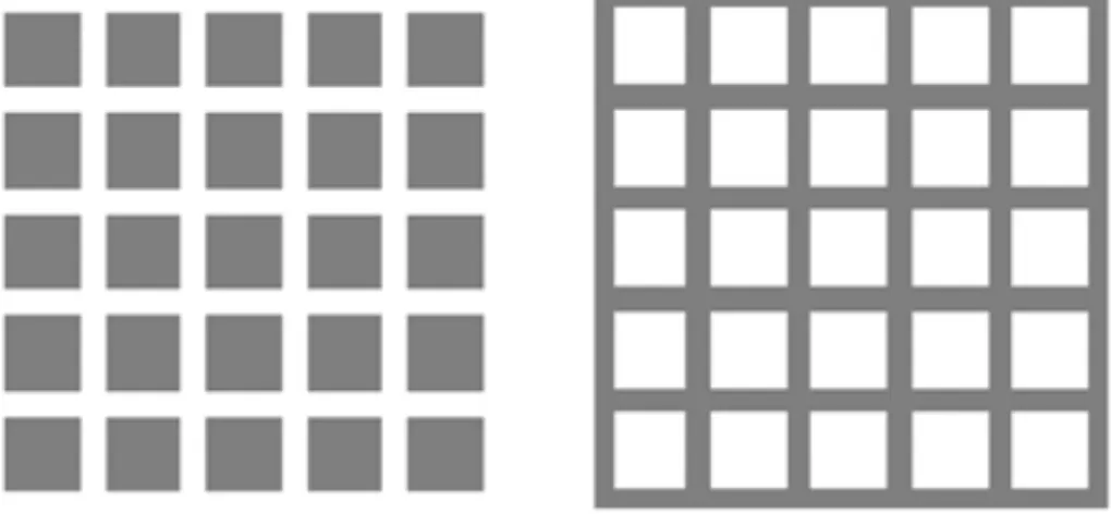
two categories as shown in Fig. 3.4 [24].
Fig. 3.4 – Basic FSS geometries: The patch-array produces a capacitive response, whereas the array of slots is inductive.
The main difference between this two cases is that we excite electric currents on the
squares while we excite "magnetic currents” in the slot square case (i.e., there is a voltage
distribution in the slots). The two cases become quite similar and symmetric if we compare
the electric field in the square case and the magnetic field in the slot square case. Following
this principle a Frequency Selective Surface is a periodic array of either radiating or
non-radiating elements or slots, which effectively act as a band stop or band, pass filter
respectively to electromagnetic waves. There are a wide variety of possible elements, which
can be used to realize FSS arrays.
3.2 Different FSS Element Types
As mentioned before FSSs can be seen as electromagnetic filters that are normally
realized using periodic structures formed by arrays of conducting elements on a dielectric
substrate or by periodic aperture elements in a conducting sheet.
The basic types of frequency selective surfaces elements are: center linked or N-pole,
type of loop, interior solid or plate type and combinations of the others elements. Fig. 3.6
Fig 3.5 – The four major groups of FSS elements. These elements may be used to construct band stop filter type FSS arrays. Elements are ordered from most narrowbanded on the left to most wide-banded on the right [25].
3.2.1 Infinite FSS Arrays
Considering the periodicity a true frequency selective surface is infinite. Thus, the
concept of starting to discuss the properties of infinite arrays and apply that knowledge for a
finite array design as in practice [24].
3.2.2 Finite FSS Array
Although only finite ones can be fabricated, the infinite FSS periodical structures are
useful to identify many of its properties. Two main considerations must be made in the design
of a finite array, i.e., edge diffraction and surface waves radiating. The edge diffraction causes
the stopband bandwidth to rise. Surface waves appear about 20-30 per cent below the
resonance, when the spacing between elements is less than 0.5λ [25]. Surface waves can be a
problem when using FSSs.
The electromagnetic band-gap structures have been employed in different to reduce
metamaterial with dispersive permeability on top of a FSS array. The HIS has a
high-impedance frequency regime and the surface wave suppression in the high high-impedance band
gap is a consequence of the FSS connected to its ground plane using a metallic via.
3.3 Metamaterial FSSs
The most common FSSs types take the form of planar, periodic metal or dielectric
arrays in 2D space. Frequency behavior of an FSS is determined by the geometry of the
surface unit cell provided that the surface size is infinite. As mentioned before FSSs were
originally introduced as spatial filters and since that they have been employed in a variety of
other applications including most recently metamaterial applications.
Metamaterial frequency selective surfaces can be used in designing reactive
impedance surfaces in a form of an artificial magnetic conductor (AMC) and electromagnetic
band-gap (EBG). The FSS are an alternative to fixed frequency metamaterial where static
geometry and spacing of unit cells to determine its frequency response. FSSs have reflective
characteristics with a certain phase and amplitude that allow frequency changes in a single
medium and are not restricted to a fixed frequency response.
The classic example of AMC is the high impedance surface described in [33]. This
high impedance surface is a periodic array printed in a dielectric substrate where each element
of the array is connected to the ground plane. This array is called mushroom. In a normal
electric conductor electric current flow is allowed, in an AMC currents will not be allowed to
travel through the medium, which in turn bans the propagation of surface waves inside the
substrate.
This metamaterial FSS will be used as a ground plane for antennas in order to
effectively suppress undesirable wave fluctuations, i.e., surface waves inside the substrate,
while producing good radiation patterns. The type of high impedance surface used in this
work is show in Fig. 3.6. The square metal patches are raised above the surface, and points at
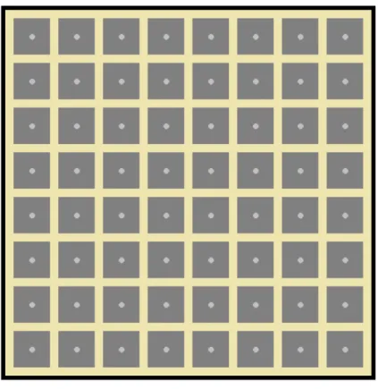
Fig. 3.6 – Superior view of a high impedance surface, patches connected to the ground plane with metal cylinders.
An AMC can be seen as a surface with increased surface impedance. Ideally the
transverse wave impedance at the surface is infinite (for an incident plane). The transverse
impedance is defined as the ratio of the transverse electric field over the transverse magnetic
field, Et/Ht. In this case an infinite impedance corresponds to Ht≈ 0, meaning that the surface
cannot bear a tangential magnetic field and hence the name magnetic conductor. The AMC
properties can the explained by the transmission line theory. Considering a λ=4 impedance
inverter, a short impedance is transformed to an open impedance. This idea is used in design
of corrugated surfaces behaving as an open circuit in terms of wave impedance, Fig. 3.7.
The HIS can be viewed as a network of parallel LC resonant circuits, which acts as a
2D electric filter to block the flow of currents and consequently suppresses the surface waves
along the sheet. When the patches are connected to the ground plane its impedance changes
and the surface waves properties are altered. The HIS equivalent LC circuit from [33] is
shown in Fig. 3.8. The capacitance occurs due to the proximity of the top metal patches, while
the inductance originates from current loops within the structure. In the LC resonance
frequency the surface impedance is high and an electromagnetic band gap is formed so waves
are not bound to the surface and the radiate into surrounding areas.
Fig. 3.8 – Origin of the equivalent circuit elements left and equivalent circuit model for the high-impedance surface right [33].
3.4 Antenna Bandwidth Augmentation
Frequency selective surfaces can be used as a superstrate to enhance the performance
of a number of antennas [34-36]. These superstrates offer the advantage of ease of fabrication
with microstrip technology and reduced thickness as compared with those of the dielectric
type superstrates. The FSS can suppress its grating lobes and as a result a high gain antenna
can be obtained.
Another way to achieve a broader bandwidth is the use of a Fabry-Pérot (FP) [37-42]
configuration. Antenna applications that require high directivity need the use of array designs
with complex feed network to comply with the directivity specifications using conventional
technology. A FP configuration uses a single radiating element instead of a array that can
simplify considerably the complexity of receivers and transmitters, reducing the size and the
mass of the conventional configurations. The FP medium consists of a capacitive-type
frequency selective surface array that is used as superstrate and an artificial magnetic
conductor as ground plane. The realized gain and the bandwidth of the antenna can be
maximum gain is increased and the bandwidth is improved when compared to the single
uniform antenna. In Chapter 6 this phenomenon will be described.
3.5 Summary
This chapter has presented a historic background and a review of literature on FSSs.
Particular emphasis has been placed on factors, which influence the FSS response, including
the element geometry, the element conductivities, the dielectric loading, and the signal
incident angles. Studies have indicated that the fundamental frequency characteristics of an
FSS are mainly governed by the element geometry, including element dimensions and shapes.
With a proper choice of element dimensions and shapes, an FSS could, to some extent, be
insensitive to incident angles and signal polarizations. Some metamaterial like FSSs were also
Chapter 4
Microstrip Antennas and Filters with
CSRR Parasitic Structures
Interference is a big issue for UWB communication systems. Since the UWB spectrum
is so large (3.1-10.6 GHz) the entire U-NII (Unlicensed National Information Infrastructure)
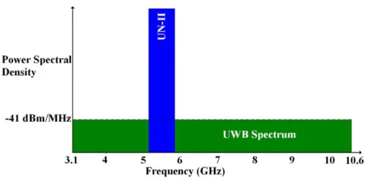
band (5.15-5.825 GHz) overlaps with its spectrum. Fig. 4.1 shows the U-NII spectrum
inserted in the UWB spectrum. As UWB transmitters must not cause electromagnetic
interference on any nearby communication systems, a solution to notch this band is needed. In
this chapter two solutions to archive a band notched function are presented.
Fig. 4.1 – Ultra wideband and UN-II spectrums.
As a first solution, a parasite metamaterial structure is inserted directly in the antennas
patch. Many UWB antennas designers have been working on several alternative solutions to
slots (arc-slot) [43], double U-slots [44], stubs or spurlines [45], square-slot [46], V-slot [47],
and attaching bar [48]. In these classical solutions the band-notched characteristic comes with
many problems mainly due to the difficulty in controlling the band-notch width in a limited
space. Some designs occupy wider band-notch (more than 2 GHz) or have only single band-
notched characteristic. The solution proposed in this work to block this band was found by
introducing a metamaterials SRR structure in the antenna’s patch for notching the entire
U-NII band. As mentioned before, a SRR is a pair of concentric annular rings splited at opposite
ends. There are two types of SRR: one were the rings are made of metal like copper and the
other is a slot-type SRR where the rings are slots on a nonmagnetic metal, which are etched in
the foursquare patch. These structures are also called Complementary Split Ring Resonator
(CSRR) where both rings have small gap between them. Different from classical solutions the
band-notch of the CSRR can be easily tunable by changing is dimensions and also have a
tunable dual band-notched characteristic.
The second solution is a microstrip UWB filter with the same goal as the first solution,
i.e., notch the UN-II band. There are many classical methods for designing such filters some
examples are the stepped-impedance resonator (SIR) [49], the spurline [50], and the defect
ground-structure [50]. The filter solutions proposed in this work consist of a simple microstrip
line backed by the CSRR placed on its ground plane. This structure present, many advantages
like a tunable band-notch by simple changing its physical dimensions, band-notch
augmentation by increasing the number of CSRRs in the ground plane and easy design and
fabrication when compared to some classic solutions
The CSRR-based medium has the property of negative effective permittivity and can
be used to reject unwanted frequency band. Due to the relatively high insertion loss for CSRR
slots, the CSRR has a band-stop filtering property. Moreover, the band-notched frequencies
can be varied by adjusting the length of C-shaped slot and the dimensions of CSRR
independently. Simulated and measured results of the proposed prototypes are provided.
4.1 – Ultra Wideband Monopole Antenna with Split Ring
Resonator as Filter
In the last years a special attention has been devoted to the development of Ultra
Wideband (UWB) monopole antennas [51 - 53]. The UWB is a short-range wireless
generally the effective isotropic radiated power (EIRP) is -41.3 dBm/MHz. The bandwidth of
the UWB signal is at least 25% of the center frequency, and the unlicensed use of UWB is in
the range of 3.1 to 10.6 GHz [54]. The use of UWB systems needs efficient antennas to
provide acceptable bandwidth requirements, and radiation pattern characteristics throughout
the designated UWB spectrum. It is generally accepted that for antennas to be classified as
ultra-wideband, the requirement will be to satisfy minimum fractional bandwidths of at least
20 % or 500 MHz or more [55].
There are many theories to explain the operation of UWB antennas. In the 1950s
Rumsey’s principle [56] was introduced to explain a family of that he called
frequency-independent antennas. This principle suggests that the impedance and pattern properties of an
antenna will be frequency independent if the antenna shape is specified only in terms of
angles. To satisfy the equal-angle requirement, the antenna configuration needs to be infinite
in principle, but is usually truncated in size in practice. This requirement makes
frequency-independent antennas quite large in terms of wavelength. It has been verified that for spiral
antennas, conic spiral antennas and some log-periodic antennas the principle can be applied.
The Rumsey’s principle was, probably, inspired by Mushiake and Uda work in the
1940s on the constant independent of self-complementary antennas for all frequencies, half
the intrinsic impedance of free space [57], which were invented by Runge in the 1930s [58].
They discovered that the product of input impedances of a planar electric current antenna
(plate) and its corresponding ‘magnetic current’ antenna (slot) was a real constant. Therefore,
an antenna built in a complementary structure of electric and magnetic currents exhibits a real
constant impedance. This theory, referred as ‘Mushiake’s relation’, has led to the
development of a large family of self-complementary antennas with constant input
impedance. Mushiake’s relation has relaxed the condition for achieving ultra wide impedance
bandwidth. However, it doesn’t guarantee constant radiation patterns over the operation
bandwidth [55]. Incidentally, an infinitely long biconic antenna was also demonstrated to
exhibit constant impedance, although it is not a self-complementary structure.
Lately, many researchers have started to look into UWB with the development of the
latest communication systems, and a surge of research interest into small UWB antennas has
been raised. Such antennas have to be small enough to be compatible to the UWB unit and
omnidirectional radiation patterns are often required for UWB terminal antennas. Finally, a
good time-domain characteristic, i.e., a good impulse response with minimal distortion is also
required for transmitting and receiving antennas. For these tasks two families of compact
![Fig. 3.8 – Origin of the equivalent circuit elements left and equivalent circuit model for the high-impedance surface right [33]](https://thumb-eu.123doks.com/thumbv2/123dok_br/15554081.96113/44.892.285.609.384.498/origin-equivalent-circuit-elements-equivalent-circuit-impedance-surface.webp)