Optical and Electrical Properties of Te Doped AlGaAsSb/AlAsSb Bragg Mirrors on InP
D. O. Toginho Filho, I. F. L. Dias, J. L. Duarte, E. Laureto,
Departamento de F´ısica, Universidade Estadual de Londrina, CP 6001, CEP 86051-970, Londrina-Paran´a, Brazil
and Jean C. Harmand
CNRS, Laboratoire de Photonique et de Nanostructures, Route de Nozay, 91460 Marcoussis, France
Received on 22 August, 2006
We present a comparative study carried out on the optical and electrical characteristics of undoped and Te doped AlGaAsSb/AlAsSb Bragg mirrors with 6.5 pairs of layers and bulk undoped and Te doped AlGaAsSb epilayers alloys lattice matched on InP, grown by molecular beam epitaxy, using SIMS, photoluminescence, reflectivity and IxV techniques. The temperature dependence of PL transitions observed in the Bragg mirrors are similar to that observed in bulk samples and associated with the donor and acceptor recombinations in alloys with electrostatic potential fluctuations described by quasi-donor-acceptor-pair (QDAP) models. We verified by SIMS the presence of a macro fluctuation in the Te profile concentrations in the growth direction of the doped Bragg mirror. The influence of doping, alloy and macrofluctuation of incorporated Te on the optical and electrical properties of doped Bragg mirror is analyzed. The AlGaAs/AlAsSb seems a very attractive option for VCSEL technology.
Keywords: Semiconductor; Bragg mirror; AlGaAs/AlAsSb
I. INTRODUCTION
Semiconductor materials of the (Al)GaAsSb family lattice matched on InP have been used for heterojunctions struc-tures employed in optoelectronic devices in the range of 1.0 µm e 2.0µm [1-3]. Due to their high refractions index con-trast systems, the Sb materials such as AlGaAsSb/AlAsSb [4] and GaAsSb/AlAsSb [5] are considered good alternatives for the preparation of distributed Bragg mirrors (DBR) [6], a key component in optoelectronic devices as vertical-cavity surface emitting lasers (VCSEL).
In ternary and quaternary alloys employed in the prepara-tion of DBRs , the phase separaprepara-tion resulting from miscibil-ity gaps induces compositional inhomogeneities in the crystal [7, 8]. The average potential depth increases with the number of components in the alloy and can act on optical and elec-trical properties of devices by creating scattering centers to transport charge carriers and/or band tails in the band gap. It is shown, for example, that the presence of Al in the quaternary AlGaAsSb alloy increases the fluctuation of the electrostatic potential in the epitaxial layer as compared to the observed in the ternary GaAsSb [9].
The required properties for DBRs are a reflectivity exceed-ing 99% and a low electrical serial resistance. High reflec-tivity is accomplished by employing materials with a high re-fractive contrast (∆n) and a sufficient number of quarter wave layers. Low electrical resistance requires a sufficiently high doping level and a low potential discontinuity∆Ec in the band conduction (∆Ev in the band valence) for n-type (p-type) [10] mirrors. However, systems with high∆n also present a high band discontinuity (∆Eg) which is not favorable to the current flow through the heterointerfaces. Raising the doping level will lower the serial resistance at the expense of an increase in free carrier absorption and a series of changes in the phys-ical properties of the semiconductor materials as a reduction in impurity ionization energy [10–12], a shift in the
funda-mental absorption edge [13–15], an increase in the density of the states in the vicinity of the band limits and a reduction in the fundamental gap [16, 17]. Then a compromise must be found to achieve the high reflectivity and the low resis-tance at the same time. High quality undoped quarter wave stacks transparent to 1.55µm wavelength were realized using AlxGa1−xAsySb1−ylattice matched to InP with x around 0.10
[18, 19]
The quaternary alloy AlxGa1−xAsySb1−y lattice matched
on InP presents a direct Γ valley for 0 ≤ x ≤ 0.40. For AlAsySb1−y lattice matched on InP the lowest conduction
band valley is the indirect X for any y value. The conduc-tion band off-set∆EC(Γ-X) in the AlGaAsSb/AlAsSb system
is approximately∼=470 meV in the typical Al concentration for Bragg mirror operating in the 1.55µm range (x ∼=0.1). A relatively high doping level and/or some metalurgical inter-vention at the interfaces in the structure are needed to improve electrical conduction.
Due to the low Al concentration required to prepare the 1.55 µm Bragg mirror with AlGaAsSb/AlAsSb, the properties of the quaternary alloy are similar to those of the ternary alloys GaAsSb. Nominally undoped GaAsSb shows non-excitonic residual acceptor impurity related to native defects as gal-lium vacancies and galgal-lium on antimony sites (VGaGaSb)with
concentrations of 1016cm−3. PL measurements on undoped
The potential fluctuations associated with the compositional inhomogeneity and/or donor and acceptor impurities can in-terfere in the transport an optical properties of the alloys em-ployed in the preparation of DBRs. Therefore the study of the electrical and optical properties of undoped and Te doped AlGaAsSb/AlAsSb Bragg mirrors compared to those of un-doped and un-doped mirror component epilayers of AlGaAsSb is important for the development of VCELs technology.
Here we report a systematic experimental work to make comparisons between the optical electrical and optical prop-erties of bulk undoped and Te doped layers of AlGaAsSb and undoped and Te doped AlGaAsSb/AlAsSb Bragg mirrors em-ploying Secondary Ion Mass Spectometry - SIMS, photolumi-nescence (PL), reflectivity and IxV measurements.
II. EXPERIMENTAL DETAILS
Undoped and Te doped AlGaAsSb/AlAsSb Bragg mirrors with 6.5 pairs were grown by MBE lattice matched on a (100) InP:Fe and (100) InP-n substrates, respectively. Te doped bulk AlGaAsSb and AlAsSb samples lattice matched on a (100) InP:Fe were also grown by MBE. The carrier concen-trations in the Te doped samples (∼=1018.cm−3) were
deter-mined by Hall measurements, at room temperature, using Van der Paw methods. Details of the sample parameters such as alloy composition, doping levels and structural parameters of Bragg mirrors can be seen in Table I.
FIG. 1: - a) Structure diagram of the Bragg mirrors; b) Potential profile diagram of the conduction band in undoped Bragg mirror; c) Potential profile diagram of the conduction band in doped Bragg mirror.
The structure of Bragg mirrors with 6.5 pairs and the con-duction band diagram for one period of undoped and Te doped
AlGaAsSb/AlAsSb samples are shown in Fig. 1a), 1b) and 1c), respectively. The band conduction alignment with the offset between Al0.1Ga0.9As0.52Sb0.48, AlAs0.56Sb0.44(X val-ley in dotted lines) and the substrate InP are also shown in Fig. 1b). The concentration profile of alloy constituents and the Te doping were obtained using SIMS.
PL measurements were performed in the temperature range of 10 K to 300 K, using the 514.5 nm line of a continuous wave Ar+laser, with different excitation intensities. Temper-ature variation was obtained by a closed-cycle helium cryo-stat. The spectral analyses of the luminescence measurements were carried out by a 0.5 m Jarrel-Ash spectrometer, coupled to a cooled InGaAs photodetector, using the standard lock-in technique.
Experimental reflectivity was measured with a Fourier transform infrared spectrometer (FTIR) in the so-called VW configuration. This configuration provided an absolute mea-surement of the reflectivity and the real shape of the reflectiv-ity spectrum with quantitative values at a 0.2% level of accu-racy.
The n-type doped Bragg mirror was metallized with Ti/Au ohmic contacts evaporated on the top and on the bottom of the sample. The sample was patterned with 100x100µm2 square mesas etched by an H2SO4:H2O2:H2O solution. The
substrate underside was thinned to 150 µm to decrease the substrate contribution to the electrical measurements. The current-voltage (IxV) dc characteristic is made by the trans-mission line method (TLM) measurement.
III. RESULTS AND DISCUSSION
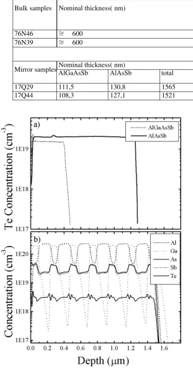
The SIMS profile of Te concentrations in bulk Te doped AlAsSb and AlGaAsSb (dotted lines) alloys prepared with similar growth conditions as that analyzed in this work is shown in Fig. 2a). The two samples show a uniform pattern for the doping level of tellurium with the depth in the growth direction. The SIMS profile of the constituent materials (Al, Ga, As, Sb, Te) of the Te doped AlGaAsSb and AlAsSb layers of Bragg mirror of 6.5 periods are presented in Fig. 2b). The incorporated Te shows a periodic fluctuation in the growth di-rection which is not observed in the bulk samples as shown in Fig. 2a). This unexpected fluctuation in the n-type dopant concentration can be associated with the growth process. The temperature of tellurium Knudsen cell in the growth cham-ber (∼=185oC) is very low when compared to the characteris-tic temperatures of Knudsen cells for other materials as Al ( ∼
TABLE I: Stoichiometric composition, thickness and Te concentration of the AlxGa1−xAsySb1−ybulk samples and AlGaAsSb/AlAsSb Bragg
mirror with 6,5 per´ıods.
Bulk samples Nominal thickness( nm) compositionAl
xGa1−xAsySb1−y Carrier concentration (cm −3)
x y
76N46 ∼= 600 0,08 0,51 undoped
76N39 ∼= 600 0,08 0,51 2,4x10¹⁸
Mirror samplesNominal thickness( nm) AlGaAsSb/ AlAsSb
AlGaAsSb AlAsSb total
17Q29 111,5 130,8 1565 0,10 0,51 undoped
17Q44 108,3 127,1 1521 0,10 0,51 3,0/1,8
FIG. 2: a) Te concentration profile in AlAsSb and AlGaAsSb doped bulk samples, growth in similar conditions at the doped bulk samples analised in this work; b) Concentration profile of the elements that compose th doped homogeneous Bragg mirror 17Q44.
Figure 3 shows the PL spectra at 10K and 300K of undoped bulk AlGaAsSb alloy (76N46) and n-type Te doped bulk Al-GaAsSb (76N39) with carrier concentration of 2.4x1018.cm−3
in comparison with PL spectra of undoped Bragg mirror (17Q29) and Te doped Bragg mirror (17Q44) with a carrier concentration of 3.0x1018.cm−3. The analyzed spectra in the Bragg mirror are related to the AlGaAsSb layers because the
ternary AlAsSb alloy is pratically transparent in the 1.55µm region. The PL spectra of undoped bulk sample (Fig. 3a) and undoped Bragg mirror (Fig. 3b) show very similar lineshape at 10K and 300K. The energy shift between the PL transitions and the broadening of emission spectrum in the Bragg mirror as compared to that obtained in the bulk alloy is a result of the higher Al concentration in the Bragg mirror (see Table I).
The PL spectra of Te doped bulk sample (Fig. 3c) and Te doped Bragg mirror (Fig. 3d)) show similar results. The PL principal peak of Bragg mirror is shifted a few meV to higher energy and show higher broadening as compared to that ob-tained for the bulk sample. This is a consequence of higher Al concentration and higher doping level in the Bragg mirror epilayers (8% Al and 2,4x1018.cm−3in the bulk versus 10 % Al and 3,0x1018.cm−3in the mirror).
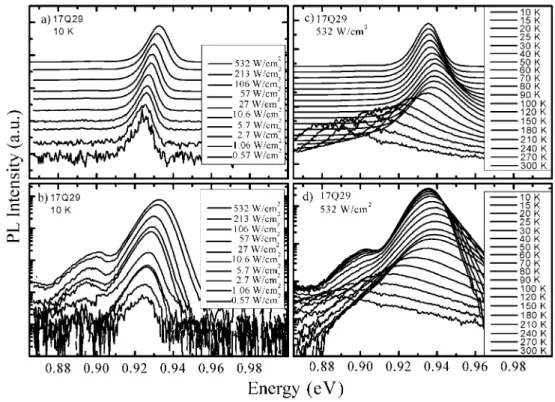
The PL spectra of undoped Bragg mirror at 10K with ex-citation intensity variation in the range 0.57 W/cm2 to 532 W/cm2 in linear and log scale are presented in Fig. 4a) and
Fig. 4b), respectively. The dominant PL transition shifts to a higher energy region with increasing excitation intensity. In PL spectra obtained at low temperature, the increase in the excitation intensity rises the number of photogenerated free carriers that screens the electrostatic potential, decreasing the amplitude of potential fluctuations and, consequently, increas-ing the energy of the emission peak. The spectra in log scale show a secondary peak at ∼=33 meV associated with a LO-phonon replica [20] below the principal transition visible for excitation intensities higher than 10.6 W/cm2. A set of PL spectra with excitation intensity fixed at 532 W/cm2recorded
at increasing temperature for the undoped Bragg mirror is shown in linear scale in the Fig. 4c) and in the log scale in Fig. 4d). The dominant PL peak energies show a characteristic inverted “S” behavior as reported elsewhere for bulk samples. The secondary peak at ∼=33 meV of the principal transition can be also seen in the log scale spectra still at 50K.
The PL spectra of Te doped Bragg mirror as a function of intensity and temperature can be seen in Fig. 5. In Figs. 5a) (linear scale) and 5b) (log scale) we have the spectra obtained at 10K with laser excitation intensity between 1.06 W/cm2and 532 W/cm2. The PL peak is very broad, suggesting the
FIG. 3: Photoluminescence curve obtained with laser intensity at 532 W/cm2and temperature between 10 K and 300 K, for samples: a) Al-GaAsSb undoped bulk (76N46); b) undoped Bragg mirror (17Q29); c) doped bulk AlGaAsSb (76N39); c) homogeneous doped Bragg mirror (17Q44).
excitation intensity of 532 W/cm2as a function of the temper-ature are shown in Fig. 5c) in a linear scale and in Fig. 5d) in a log scale. The set of PL spectra in the linear scale shows an explicit “S” behavior for the dominant transition with in-creasing temperature similar to that observed for undoped and Te doped bulk samples of antimony family epilayers analyzed elsewhere [21]. The PL spectra presented indicate two tran-sitions, one with lower energy peak transition more intense at higher temperatures.
The temperature dependence of the PL dominant peak en-ergies of undoped (76N46), Te doped (76N39) bulk samples and undoped (17Q29) and Te doped (17Q44) Bragg mirrors in the 10K-300K range for intensity excitation of 532 W/cm2 are shown in Fig. 6a). The temperature dependence of dom-inant transitions in undoped samples is very similar, showing a weak blue shift (1-2 meV) at low temperatures (T<100K). The behavior of the PL peak energies of Te doped bulk al-loy as a function of the temperature shows a weak “S” pattern with the first red shift of∼=4 meV until T∼=50K. The peak en-ergy of n-type AlGaAsSb layers in the Te doped Bragg mirror shows a stronger “S” behavior with the first red shift of ∼=13 meV to T∼=50K. The “red/blue/red” behavior is characteristic
of materials with electrostatic fluctuations and is stronger as the amplitude of the potential fluctuation grows. This effect can be observed in undoped GaAsSb and AlGaAsSb samples [9]. The presence of Al in the quaternary alloy increases the fluctuation of the electrostatic fluctuation, increasing the vari-ation of recombinvari-ation energies as a function of temperature thus decreasing intensity excitations at low temperatures and reinforcing the “S” behavior. Here the presence of the unex-pected macro fluctuation in the incorporated Te observed by SIMS in the doped Bragg mirror can explain the stronger “S” behavior in the temperature dependence of PL transitions.
Figure 6b) shows the temperature dependence of the FWHM (Full Width Half Maximum) in all samples. The doped samples shows a stronger broadening (∼=40 meV) as compared to that observed for undoped samples. The FWHM of the emission spectra of all samples shows an increas-ing broadenincreas-ing in the 10K-300K temperature interval. The stronger broadening observed for undoped Bragg mirror as compared to the undoped AlGaAsSb layer can be associated to the higher Al concentration in the quaternary layer of the mirror. The behavior of FWHM as a function of the tempera-ture, in the two doped samples present some differences. The FWHM of the doped layer is very similar to that of the un-doped with increasing temperature. The FWHM of the Bragg mirror shows a gradual increasing with increasing tempera-ture, reaching a plateau in the temperature range between 50K and 100K and increasing again after the plateau. The plateau observed indicates two competing recombination channels in the respective temperature range. One channel is dominant at the low temperature limit and the other is dominant at the high temperature limit. This is a characteristic behavior of the competition between donor-acceptor-pair or a quasi-donor-acceptor-pair transitions and free to bound transitions with increasing temperatures discussed more systematically else-where for the antimony family [9].
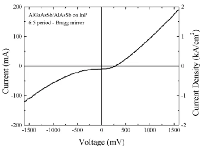
Reflectivity measurements for both undoped and doped Bragg mirrors are shown in Fig. 7. Results show that even for a small number of periods it is possible to obtain a rel-atively high reflectivity and a wide stop band for the Al-GaAsSb/AlAsSb system. This is associated with the high in-dex contrast (∼=0.54) between the quaternary and ternary al-loys. The highest reflectivity (widest stop band) was obtained for the undoped Bragg mirror, however the reflectivity differ-ence is not very large between the two mirrors changing from 0.91 (0.39µm) for the undoped mirror to 0.90 (0.37µm) for the doped mirror. The decrease in reflectivity in the doped sample is associated with a free carrier absorption due to the presence of Te.
dis-FIG. 4: Photoluminescence curve with laser intensity and temperature dependences, for undoped Bragg mirror sample (17Q29).
FIG. 5: Photoluminescence curve with laser intensity and temperature dependences, for doped Bragg mirror sample (17Q44).
turbance in the conduction and valence band edges causing strong electrostatic fluctuations and/or scattering centers that can also contribute to an increase in serial resistance. The non-completely ohmic character of the IxV curve can be associated with several factors such as the asymmetric incorporation of Te, higher at the end of the quaternary layer due to
FIG. 6: Energy and FWHM dependences of main peak of PL with the temperature, for undoped bulk AlGaAsSb (76N46), doped bulk Al-GaAsSb (76N39), undoped Bragg mirror (17Q29) and doped Bragg mirror (17Q44), obtained with laser intensity at 532 W/cm2.
FIG. 7: Reflectivity curves for DBRs samples with 6,5 periods, ob-tained at 300 K.
FIG. 8: Current x Voltage curve of the homogeneous doped Bragg mirror (17Q44) at 300 K.
also optimized to improve the reflectivity and conduction pa-rameters.
IV. CONCLUSION
We have investigated Bragg mirrors of undoped and Te doped AlGaAsSb/AlAsSb system with 6.5 periods and un-doped and Te un-doped bulk samples of AlGaAsSb using SIMS, photoluminescence, reflectivity and IxV measurements. The optical transitions in the PL spectra of AlGaAsSb layers in undoped and Te doped Bragg mirror show similar behavior and lineshape to that found in bulk samples of undoped and Te doped AlGaAsSb. The optical transitions are associated with donor and acceptor recombinations in alloys with poten-tial fluctuations consistent with the quasi-donor-acceptor-pair (QDAP) model. The macrofluctuations in the incorporated Te, associated probably with the growth process, introduce another source of disturbance that intensify the electrostatic potential fluctuation in addition to the characteristic edge band variations given by the alloy and by doping raising the ampli-tude of the “S” behavior. The presence of macrofluctuations in the dopant incorporations can also generate alternative re-combination channels and/or scattering centers harmful to the optical and electrical properties of the Bragg mirrors. More-over, the asymmetric pattern of the dopant incorporation can facilitate the electron conduction in one direction.
Acknowledgements
The authors wish to thank the financial
sup-port granted by the Brazilian agencies CAPES, CNPq, Fundac¸˜ao Arauc´aria and FBB.
[1] B. Lambert, Y. Toudic, Y. Rouillard, M. Baudet, B. Guenais, B. Deveaud, I. Valiente, and J. C. Simon, Appl. Phys. Lett.64, 690 (1994).
[2] O. Blum, I. J. Fritz, L. R. Dawson, and T. J. Drummond, Elec-tron. Lett.31, 1247 (1995).
[3] N. Kuze, H. Goto, M. Matsui, I. Shibasaki, and H. Sakaki, J. Cryst. Growth175/176, 868 (1997).
[4] D. O. Toginho Filho, I. F. L. Dias, J.L.Duarte, S. A. Lourenc¸o, L. C. Poc¸as, E. Laureto, J. C. Harmand, Superlattices Mi-crostruct.31, 277 (2002).
[5] F. Genty, G. Almuneau, L. Chusseau, Wilk, S. Gaillard G. Boissier, P. Grech, and J. Jacquet, J. Cryst. Growth201/202, 1024 (1999).
[6] I. F. L. Dias, B. Nabet, A. Kohl, and J. C. Harmand, Electron. Lett.33, 716 (1997).
[7] T. H. Chiu, W. T. Tsang, S. N. G. Chu, J. Shah, and J. A. Ditzen-berger, Appl. Phys. Lett.46, 408 (1985).
[8] B. Shin, A. Lin, K. Lappo, R. S. Goldman, M. C. Hanna, S. Francoeur, A. G. Norman, and A. Mascarenhas, Appl. Phys. Lett.80, 3292 (2002).
[9] D. O. Toginho Filho, I. F. L. Dias, E. Laureto, J. L. Duarte, S.
A. Lourenc¸o, L. C. Poc¸as, S. S. Prabhu, and J. Klem, J. Appl. Phys.97, 123702 (2005).
[10] J. B. Krieger, and M Nightingale, Phys. Rev. B4, 1266 (1971). [11] N. F. Mott, Proc.Phys. Soc. (London)62, 419 (1949).
[12] N. F. Mott, Rev. Mod. Phys.40, 677 (1968). [13] E. Burstein, Phys. Rev.93, 632 (1954).
[14] T. S. Moss, Proc.Phys. Soc. (London) B76, 775 (1954). [15] J. I. Pankove, and P. Aigrain, Phys. Rev.126, 956 (1962). [16] R. A. Abram, G.J.Rees, and B.L.H. Wilson, Adv. Phys.27, 799
(1978).
[17] K. F. Berggren, and B. E. Sernelius, Phys. Rev. B24, 1971 (1981).
[18] J. C. Harmand, Kohl, M. Juhel, and G. Le Roux, J. Cryst. Growth175, 372 (1997).
[19] L. Chusseau, G. Almuneau, and F. Genty, Recent Research de-velopments in Quantum Electronics1, 85 (1999).
[20] P. S. Dutta, H. L. Bhat, and V. Kumar, J. Appl. Phys.81, 5821 (1997).